VS-1N1...A, VS-1N36..A Series
www.vishay.com
Vishay Semiconductors
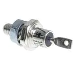
Medium Power Silicon Rectifier Diodes, (Stud Version), 12 A
FEATURES
• Voltage ratings from 50 V to 1000 V
• High surge capability
• Low thermal impedance
• High temperature rating
• Can be supplied as JAN and JAN-TX devices in
accordance with MIL-S-19500/260
DO-4 (DO-203AA)
• Material categorization: for definitions of compliance
please see www.vishay.com/doc?99912
PRIMARY CHARACTERISTICS
IF(AV)
12 A
Package
DO-4 (DO-203AA)
Circuit configuration
Single
MAJOR RATINGS AND CHARACTERISTICS
PARAMETER
TEST CONDITIONS
IF(AV)
TC
50 Hz
60 Hz
50 Hz
60 Hz
IFSM
I2t
TJ
Range
VRRM
Note
• JEDEC® registered values are in bold
VALUES
12
150
230
240
260
240
-65 to +200
50 to 1000
UNITS
A
°C
A
A2s
°C
V
ELECTRICAL SPECIFICATIONS
VOLTAGE RATINGS
TYPE NUMBER
VRRM, MAXIMUM
REPETITIVE PEAK
REVERSE VOLTAGE
(TC = -65 °C TO 200 °C)
V
VR(RMS), MAXIMUM RMS
REVERSE VOLTAGE
(TC = -65 °C TO 200 °C)
V
VRSM, MAXIMUM
NON-REPETITIVE PEAK
REVERSE VOLTAGE
(TC = -65 °C TO 200 °C)
V
VS-1N1199A
50
35
100
VS-1N1200A
100
70
200
VS-1N1201A
150
105
300
VS-1N1202A
200
140
350
VS-1N1203A
300
210
450
VS-1N1204A
400
280
600
VS-1N1205A
500
350
700
VS-1N1206A
600
420
800
VS-1N3670A
700
490
900
VS-1N3671A
800
560
1000
VS-1N3672A
900
630
1100
VS-1N3673A
1000
700
1200
VS-1N3624
1000
1200
1400
Notes
• JEDEC® registered values are in bold
• Basic part number indicates cathode to case; for anode to case, add “R” to part number, e.g., 1N1199RA
VRM, MAXIMUM DIRECT
REVERSE VOLTAGE
(TC = -65 °C TO 200 °C)
V
50
100
150
200
300
400
500
600
700
800
900
1000
1000
Revision: 11-Jan-18
Document Number: 93493
1
For technical questions within your region: DiodesAmericas@vishay.com, DiodesAsia@vishay.com, DiodesEurope@vishay.com
THIS DOCUMENT IS SUBJECT TO CHANGE WITHOUT NOTICE. THE PRODUCTS DESCRIBED HEREIN AND THIS DOCUMENT
ARE SUBJECT TO SPECIFIC DISCLAIMERS, SET FORTH AT www.vishay.com/doc?91000
�VS-1N1...A, VS-1N36..A Series
www.vishay.com
Vishay Semiconductors
FORWARD CONDUCTION
PARAMETER
SYMBOL
Maximum average forward current
at case temperature
IF(AV)
Maximum peak one cycle non-repetitive
surge current
IFSM
Maximum I2t for fusing
I2t
TEST CONDITIONS
180° sinusoidal conduction
Half cycle 50 Hz sine wave
or 6 ms rectangular pulse
Half cycle 60 Hz sine wave
or 5 ms rectangular pulse
Half cycle 50 Hz sine wave
or 6 ms rectangular pulse
Half cycle 60 Hz sine wave
or 5 ms rectangular pulse
t = 10 ms
t = 8.3 ms
t = 10 ms
t = 8.3 ms
I2t
Maximum
for individual
device fusing
Maximum I2t for individual
device fusing
Maximum forward voltage drop
VRRM = 50 V
VRRM = 100 V
VRRM = 150 V
VRRM = 200 V
VRRM = 300 V
VRRM = 400 V
Maximum average
reverse current
VRRM = 500 V
VRRM = 600 V
VRRM = 700 V
VRRM = 800 V
VRRM = 900 V
VRRM = 1000 V
I2t (1)
VFM
IR(AV) (2)
VALUES
12
150
Following any rated load
condition and with rated
VRRM applied
230
Following any rated load
condition and with VRRM
applied following surge = 0 V
275
UNITS
A
°C
240
A
285
With rated VRRM applied
following surge,
initial TJ = 200 °C
260
With VRRM = 0 V following
surge, initial TJ = 200 °C
370
340
240
A2s
t = 0.1 ms to 10 ms, VRRM = 0 V following surge
3715
A2s
IF(AV) = 12 A (38 A peak), TC = 25 °C
1.35
3.0
2.5
2.25
2.0
1.75
1.5
1.25
1.0
0.9
0.8
0.7
0.6
V
Maximum rated IF(AV) and TC
mA
Notes
• JEDEC® registered values are in bold
(1) I2t for time t = I2t x t
x
x
(2) Maximum peak reverse current (I
RM) under same conditions 2 x rated IR(AV)
THERMAL AND MECHANICAL SPECIFICATIONS
PARAMETER
Maximum operating case and
storage temperature range
Maximum internal thermal
resistance, junction to case
Thermal resistance,
case to sink
minimum
maximum
minimum
Mounting torque
maximum
minimum
maximum
SYMBOL
TEST CONDITIONS
TC, TStg
UNITS
-65 to 200
°C
RthJC
DC operation
2.0
RthCS
Mounting surface, smooth, flat and greased
0.5
°C/W
Torque applied to nut; non-lubricated threads
Torque applied to nut; lubricated threads
Torque applied to device case; lubricated threads
Approximate weight
Case style
VALUES
JEDEC®
1.36 (12)
1.69 (15)
1.07 (9.45)
N·m
(lbf · in)
1.30 (11.55)
1.17 (10.35)
1.43 (12.65)
7.0
g
0.25
oz.
DO-4 (DO-203AA)
Note
• JEDEC registered values are in bold
Revision: 11-Jan-18
Document Number: 93493
2
For technical questions within your region: DiodesAmericas@vishay.com, DiodesAsia@vishay.com, DiodesEurope@vishay.com
THIS DOCUMENT IS SUBJECT TO CHANGE WITHOUT NOTICE. THE PRODUCTS DESCRIBED HEREIN AND THIS DOCUMENT
ARE SUBJECT TO SPECIFIC DISCLAIMERS, SET FORTH AT www.vishay.com/doc?91000
�VS-1N1...A, VS-1N36..A Series
220
Vishay Semiconductors
IF - Instantaneous Forward Current (A)
Maximum Allowable Case Temperature (°C)
www.vishay.com
Conduction Period
200
180
160
DC
140
+180 °C
Wave
120 +180 °C
Wave
+120 °C
&
100 Wave
+60 °C
&
Wave
0
0
2
4
6
8
10
12
14
16
18
20
2
102
5
2
TJ = 200 °C
2
1.0
0
ZthJC - Transient Thermal Impedance (°C/W)
Wave
Wave
8
+120 °C
+60 °C
&
&
Wave
Wave
DC
6
TJ = 200°C
Conduction Period
4
2
0
0
2
4
6
8
10
Average Forward Current Over Full Cycle (A)
104
5
5
2
2
DC
5
+120 °C
+120 °C
2
1.0
1.0
&
&
Wave
Wave
103
5
Wave
Wave
2
TJ = 200°C
Conduction Period
2
5 10
2
5 102
2
2.0
2.5
3.0
3.5
2
102
5 103
Average Forward Current Over Full Cycle (A)
Fig. 3 - Maximum High Level Forward Power Loss vs.
Average Forward Current
Steady State Value = 2.0 °C/W
1.0
5
2
10-1
5
2
10-2
10-4 2 5 10-3
2 5 10-2 2 5 10-1 2 5 1
2 5 10
t - Square Wave Pulse Duration (s)
Fig. 5 - Maximum Transient Thermal Impedance,
Junction to Case vs. Pulse Duration
Peak Half Sine Wave Forward Current (A)
Average Forward Power Loss
Over Full Cycle (W)
102
+180 °C
+180 °C
1.5
10
5
Fig. 2 - Maximum Low Level Forward Power Loss vs.
Average Forward Current
10
1.0
Instantaneous Forward Voltage (V)
12
+180 °C
+180 °C
0.5
Fig. 4 - Maximum Forward Voltage vs. Forward Current
14
10
25 °C
10
5
Average Forward Current Over Full Cycle (A)
Fig. 1 - Average Forward Current vs.
Maximum Allowable Case Temperature
Average Forward Power Loss
Over Full Cycle (W)
103
5
300
At Any Rated Load Condition And With
Rated VRRM Applied Following Surge
200
60 Hz
100
0
1 1
50 Hz
2
4
6 8 10
20
40 60
Number Of Equal Amplitude
Half Cycle Current Pulses (N)
Fig. 6 - Maximum Non-Repetitive 50 Hz Surge Current vs.
Number of Current Pulses
LINKS TO RELATED DOCUMENTS
Dimensions
www.vishay.com/doc?95311
Revision: 11-Jan-18
Document Number: 93493
3
For technical questions within your region: DiodesAmericas@vishay.com, DiodesAsia@vishay.com, DiodesEurope@vishay.com
THIS DOCUMENT IS SUBJECT TO CHANGE WITHOUT NOTICE. THE PRODUCTS DESCRIBED HEREIN AND THIS DOCUMENT
ARE SUBJECT TO SPECIFIC DISCLAIMERS, SET FORTH AT www.vishay.com/doc?91000
�Outline Dimensions
Vishay Semiconductors
DO-203AA (DO-4)
DIMENSIONS in millimeters (inches)
+ 0.3
0
+ 0.01
(0.08
0)
0.8 ± 0.1
(0.03 ± 0.004)
3.30 (0.13)
4.00 (0.16)
2
5.50 (0.22) MIN.
R 0.40
R (0.02)
Ø 1.80 ± 0.20
(Ø 0.07 ± 0.01)
20.30 (0.80) MAX.
Ø 6.8 (0.27)
10.20 (0.40)
MAX.
3.50 (0.14)
11.50 (0.45)
10.70 (0.42)
10/32" UNF-2A
For metric devices: M5 x 0.8
11 (0.43)
Document Number: 95311
Revision: 30-Jun-08
For technical questions, contact: indmodules@vishay.com
www.vishay.com
1
�Legal Disclaimer Notice
www.vishay.com
Vishay
Disclaimer
ALL PRODUCT, PRODUCT SPECIFICATIONS AND DATA ARE SUBJECT TO CHANGE WITHOUT NOTICE TO IMPROVE
RELIABILITY, FUNCTION OR DESIGN OR OTHERWISE.
Vishay Intertechnology, Inc., its affiliates, agents, and employees, and all persons acting on its or their behalf (collectively,
“Vishay”), disclaim any and all liability for any errors, inaccuracies or incompleteness contained in any datasheet or in any other
disclosure relating to any product.
Vishay makes no warranty, representation or guarantee regarding the suitability of the products for any particular purpose or
the continuing production of any product. To the maximum extent permitted by applicable law, Vishay disclaims (i) any and all
liability arising out of the application or use of any product, (ii) any and all liability, including without limitation special,
consequential or incidental damages, and (iii) any and all implied warranties, including warranties of fitness for particular
purpose, non-infringement and merchantability.
Statements regarding the suitability of products for certain types of applications are based on Vishay's knowledge of typical
requirements that are often placed on Vishay products in generic applications. Such statements are not binding statements
about the suitability of products for a particular application. It is the customer's responsibility to validate that a particular product
with the properties described in the product specification is suitable for use in a particular application. Parameters provided in
datasheets and / or specifications may vary in different applications and performance may vary over time. All operating
parameters, including typical parameters, must be validated for each customer application by the customer's technical experts.
Product specifications do not expand or otherwise modify Vishay's terms and conditions of purchase, including but not limited
to the warranty expressed therein.
Hyperlinks included in this datasheet may direct users to third-party websites. These links are provided as a convenience and
for informational purposes only. Inclusion of these hyperlinks does not constitute an endorsement or an approval by Vishay of
any of the products, services or opinions of the corporation, organization or individual associated with the third-party website.
Vishay disclaims any and all liability and bears no responsibility for the accuracy, legality or content of the third-party website
or for that of subsequent links.
Except as expressly indicated in writing, Vishay products are not designed for use in medical, life-saving, or life-sustaining
applications or for any other application in which the failure of the Vishay product could result in personal injury or death.
Customers using or selling Vishay products not expressly indicated for use in such applications do so at their own risk. Please
contact authorized Vishay personnel to obtain written terms and conditions regarding products designed for such applications.
No license, express or implied, by estoppel or otherwise, to any intellectual property rights is granted by this document or by
any conduct of Vishay. Product names and markings noted herein may be trademarks of their respective owners.
© 2022 VISHAY INTERTECHNOLOGY, INC. ALL RIGHTS RESERVED
Revision: 01-Jan-2022
1
Document Number: 91000
�