VS-70TPS12PbF, VS-70TPS16PbF High Voltage Series
www.vishay.com
Vishay Semiconductors
Thyristor High Voltage, Phase Control SCR, 70 A
FEATURES
2
(A)
• High surge capability
• High voltage input rectification
• Designed and qualified
JEDEC®-JESD 47
1
2
3
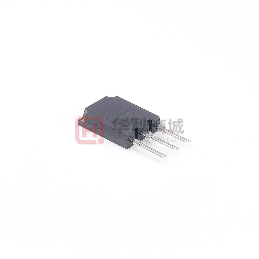
Super TO-247
1 (K)
(G) 3
according
to
• Material categorization:
for definitions of compliance please see
www.vishay.com/doc?99912
APPLICATIONS
PRIMARY CHARACTERISTICS
IT(AV)
70 A
VDRM/VRRM
1200 V, 1600 V
VTM
1.25 V
IGT
100 mA
TJ
-40 °C to +125 °C
Package
Super TO-247
Circuit configuration
Single SCR
• AC switches
• High voltage input rectification (soft start)
• High current crow-bar
• Other phase-control circuits
• Designed to be used with Vishay input diodes, switches,
and output rectifiers which are available in identical
package outlines
DESCRIPTION
The VS-70TPS.. PbF high voltage series of silicon controlled
rectifiers are specifically designed for high and medium
power switching, and phase control applications.
MAJOR RATINGS AND CHARACTERISTICS
PARAMETER
TEST CONDITIONS
VALUES
IT(AV)
Sinusoidal waveform
70
IRMS
Lead current limitation
75
VRRM/VDRM
Range
ITSM
VT
100 A, TJ = 25 °C
UNITS
A
1200 to 1600
V
1100
A
1.4
V
dV/dt
500
V/μs
dI/dt
150
A/μs
-40 to +125
°C
IRRM/IDRM
AT 125 °C
mA
TJ
VOLTAGE RATINGS
PART NUMBER
VRRM/VDRM, MAXIMUM
REPETITIVE PEAK AND
OFF-STATE VOLTAGE
V
VRSM, MAXIMUM
NON-REPETITIVE PEAK
REVERSE VOLTAGE
V
VS-70TPS12PbF
1200
1300
VS-70TPS16PbF
1600
1700
15
Revision: 05-Jun-2020
Document Number: 94391
1
For technical questions within your region: DiodesAmericas@vishay.com, DiodesAsia@vishay.com, DiodesEurope@vishay.com
THIS DOCUMENT IS SUBJECT TO CHANGE WITHOUT NOTICE. THE PRODUCTS DESCRIBED HEREIN AND THIS DOCUMENT
ARE SUBJECT TO SPECIFIC DISCLAIMERS, SET FORTH AT www.vishay.com/doc?91000
�VS-70TPS12PbF, VS-70TPS16PbF High Voltage Series
www.vishay.com
Vishay Semiconductors
ABSOLUTE MAXIMUM RATINGS
PARAMETER
Maximum average on-state current
Maximum continuous RMS on-state
current as AC switch
Maximum peak, one-cycle
non-repetitive surge current
Maximum I2t for fusing
Maximum I2t for fusing
SYMBOL
IT(AV)
IT(RMS)
ITSM
I2t
I2t
Low level value of threshold voltage
VT(TO)1
High level value of threshold voltage
VT(TO)2
Low level value of on-state slope resistance
rt1
High level value of on-state slope resistance
rt2
TEST CONDITIONS
VALUES UNITS
TC = 82 °C, 180° conduction half sine wave
70
Lead current limitation
75
10 ms sine pulse, rated VRRM applied
930
10 ms sine pulse, no voltage reapplied
10 ms sine pulse, rated VRRM applied
A
1100
Initial TJ = TJ
maximum
10 ms sine pulse, no voltage reapplied
t = 0.1 ms to 10 ms, no voltage reapplied
4325
6115
61 150
0.916
1.21
TJ = 125 °C
4.138
3.43
A2s
A2s
V
m
Maximum peak on-state voltage
VTM
100 A, TJ = 25 °C
1.4
V
Maximum rate of rise of turned-on current
dI/dt
TJ = 25 °C
150
A/μs
Maximum holding current
IH
Anode supply = 6 V, resistive load, initial IT = 1 A, TJ = 25 °C
200
Maximum latching current
IL
Anode supply = 6 V, resistive load, TJ = 25 °C
400
TJ = 25 °C
1.0
Maximum reverse and direct leakage current IRRM/IDRM
Maximum rate of rise of off-state voltage
dV/dt
TJ = 125 °C
TJ = 125 °C
VR = rated VRRM/VDRM
(TJ = TJ max., linear to 80 %
VDRM = Rg- k = open)
mA
15
500
V/μs
TRIGGERING
PARAMETER
Maximum peak gate power
Maximum average gate power
Maximum peak gate current
Maximum peak negative gate voltage
SYMBOL
PGM
PG(AV)
TEST CONDITIONS
10
T = 30 μs
2.5
IGM
2.5
-VGM
10
TJ = - 40 °C
Maximum required DC gate voltage to trigger
Maximum required DC gate current to trigger
VALUES UNITS
VGT
IGT
TJ = 25 °C
1.8
Anode supply = 6 V resistive load
TJ = 125 °C
1.1
TJ = - 40 °C
150
TJ = 25 °C
Anode supply = 6 V resistive load
TJ = 125 °C
Maximum DC gate voltage not to trigger
VGD
Maximum DC gate current not to trigger
IGD
1.5
TJ = 125 °C, VDRM = rated value
100
W
A
V
mA
80
0.25
V
6
mA
Revision: 05-Jun-2020
Document Number: 94391
2
For technical questions within your region: DiodesAmericas@vishay.com, DiodesAsia@vishay.com, DiodesEurope@vishay.com
THIS DOCUMENT IS SUBJECT TO CHANGE WITHOUT NOTICE. THE PRODUCTS DESCRIBED HEREIN AND THIS DOCUMENT
ARE SUBJECT TO SPECIFIC DISCLAIMERS, SET FORTH AT www.vishay.com/doc?91000
�VS-70TPS12PbF, VS-70TPS16PbF High Voltage Series
www.vishay.com
Vishay Semiconductors
THERMAL AND MECHANICAL SPECIFICATIONS
PARAMETER
SYMBOL
TEST CONDITIONS
VALUES
Maximum junction temperature range
TJ
-40 to +125
Maximum storage temperature range
TStg
-40 to +150
Maximum thermal resistance,
junction to case
RthJC
Maximum thermal resistance,
junction to ambient
RthJA
Typical thermal resistance,
case to heatsink
RthCS
DC operation
°C
0.27
°C/W
40
Mounting surface, smooth and greased
0.2
6
g
0.21
oz.
minimum
6 (5)
maximum
12 (10)
kgf · cm
(lbf · in)
Approximate weight
Mounting torque
UNITS
Marking device
70TPS12
Case style Super TO-247
70TPS16
RthJ-hs CONDUCTION PER JUNCTION
SINE HALF WAVE CONDUCTION
DEVICE
VS-70TPS..PbF
RECTANGULAR WAVE CONDUCTION
180°
120°
90°
60°
30°
180°
120°
90°
60°
30°
0.078
0.092
0.117
0.172
0.302
0.053
0.092
0.125
0.180
0.306
UNITS
°C/W
130
RthJC (DC) = 0.27 ˚C/W
120
110
Conduction Angle
30˚
100
60˚
90
90˚
120˚
180˚
80
70
0
10 20 30 40 50 60 70 80
Maximum Allowable Case Temperature (°C)
Maximum Allowable Case Temperature (°C)
Note
• The table above shows the increment of thermal resistance RthJ-hs when devices operate at different conduction angles than DC
130
RthJC (DC) = 0.27 ˚C/W
120
DC
110
Conduction Period
100
180˚
90
80
30˚
70
60˚
90˚
120˚
60
0
10 20 30 40 50 60 70 80 90
Average On-state Current (A)
Average On-state Current (A)
Fig. 1 - Current Rating Characteristics
Fig. 2 - Current Rating Characteristics
Revision: 05-Jun-2020
Document Number: 94391
3
For technical questions within your region: DiodesAmericas@vishay.com, DiodesAsia@vishay.com, DiodesEurope@vishay.com
THIS DOCUMENT IS SUBJECT TO CHANGE WITHOUT NOTICE. THE PRODUCTS DESCRIBED HEREIN AND THIS DOCUMENT
ARE SUBJECT TO SPECIFIC DISCLAIMERS, SET FORTH AT www.vishay.com/doc?91000
�VS-70TPS12PbF, VS-70TPS16PbF High Voltage Series
Vishay Semiconductors
1000
140
180˚
120˚
90˚
60˚
30˚
120
100
80
RMS Limit
60
40
Conduction Angle
800
700
600
500
20
VS-70TPS.. Series
Tj = 125˚C
400
0
0
10
20
30
40
50
60
70
1
10
100
Number of Equal Amplitude Half Cycle
Current Pulses (N)
Average On-state Current (A)
Fig. 3 - On-State Power Loss Characteristics
Fig. 5 - Maximum Non-Repetitive Surge Current
150
1200
180˚
120˚
90˚
60˚
30˚
120
90
Maximum non-repetitive surge current
versus pulse train duration.
Initial TJ = 125 °C
No voltage reapplied
Rated VRRM reapplied
1100
Peak Half Sine Wave
Forward Current (A)
Maximum Average On-state Power Loss (W)
At any rated load condition and with
rated VRRM applied following surge.
Initial TJ = 125 °C
at 60 Hz 0.0083 s
at 50 Hz 0.0100 s
900
Peak Half Sine Wave
Forward Current (A)
Maximum Average On-state Power Loss (W)
www.vishay.com
DC
RMS Limit
60
Conduction Period
30
1000
900
800
700
600
500
400
Tj = 125˚C
0
0
15
30
45
60
300
0.01
75
0.1
1
10
Average On-state Current (A)
Pulse Train Duration (s)
Fig. 4 - On-State Power Loss Characteristics
Fig. 6 - Maximum Non-Repetitive Surge Current
Instantaneous On-state Current (A)
1000
Tj = 125˚C
100
10
Tj = 25˚C
1
0.5
1
1.5
2
2.5
3
3.5
Instantaneous On-state Voltage (V)
Fig. 7 - On-State Voltage Drop Characteristics
Revision: 05-Jun-2020
Document Number: 94391
4
For technical questions within your region: DiodesAmericas@vishay.com, DiodesAsia@vishay.com, DiodesEurope@vishay.com
THIS DOCUMENT IS SUBJECT TO CHANGE WITHOUT NOTICE. THE PRODUCTS DESCRIBED HEREIN AND THIS DOCUMENT
ARE SUBJECT TO SPECIFIC DISCLAIMERS, SET FORTH AT www.vishay.com/doc?91000
�VS-70TPS12PbF, VS-70TPS16PbF High Voltage Series
www.vishay.com
10
Rectangular gate pulse
a) Recommended load line for
rated diF/dt: 20 V, 30 Ω
tr = 0.5 μs, tp > = 6 μs
(1) PGM = 100 W, tp = 500 μs
(2) PGM = 50 W, tp = 1 ms
(3) PGM = 20 W, tp = 25 ms
(4) PGM = 10 W, tp = 5 ms
b) Recommended load line for
< = 30 % rated diF/dt: 20 V, 65 Ω
tr = 1 μs, tp > = 6 μs
(a)
(b)
VGD
TJ = - 40 °C
TJ = 25 °C
1
TJ = 125 °C
Instantaneous Gate Voltage (V)
100
Vishay Semiconductors
0.01
(2)
(1)
Frequency Limited by PG(AV)
IGD
0.1
0.001
(3)
(4)
0.1
1
10
100
1000
Instantaneous Gate Current (A)
Transient Thermal Impedance ZthJC (°C/W)
Fig. 8 - Gate Characteristics
1
Steady State Value
(DC Operation)
0.1
D = 0.50
D = 0.33
D = 0.25
D = 0.17
D = 0.08
Single Pulse
70TPS.. Series
0.01
0.0001
0.001
0.01
0.1
Square Wave Pulse Duration (s)
1
10
Fig. 9 - Thermal Impedance ZthJC Characteristics
Revision: 05-Jun-2020
Document Number: 94391
5
For technical questions within your region: DiodesAmericas@vishay.com, DiodesAsia@vishay.com, DiodesEurope@vishay.com
THIS DOCUMENT IS SUBJECT TO CHANGE WITHOUT NOTICE. THE PRODUCTS DESCRIBED HEREIN AND THIS DOCUMENT
ARE SUBJECT TO SPECIFIC DISCLAIMERS, SET FORTH AT www.vishay.com/doc?91000
�VS-70TPS12PbF, VS-70TPS16PbF High Voltage Series
www.vishay.com
Vishay Semiconductors
ORDERING INFORMATION TABLE
Device code
VS-
70
T
P
S
16
PbF
1
2
3
4
5
6
7
1
-
Vishay Semiconductors product
2
-
Current rating (70 = 70 A)
3
-
Circuit configuration:
T = thyristor
4
-
Package:
5
-
6
-
Voltage code x 100 = VRRM
7
-
PbF = lead (Pb)-free
P = super TO-247
Type of silicon:
S = standard recovery rectifier
12 = 1200 V
16 = 1600 V
ORDERING INFORMATION (example)
PREFERRED P/N
QUANTITY PER T/R
MINIMUM ORDER QUANTITY
PACKAGING DESCRIPTION
VS-70TPS12PbF
25
500
Antistatic plastic tube
VS-70TPS16PbF
25
500
Antistatic plastic tube
LINKS TO RELATED DOCUMENTS
Dimensions
www.vishay.com/doc?95073
Part marking information
www.vishay.com/doc?95070
SPICE model VS-70TPS12
www.vishay.com/doc?96760
SPICE model VS-70TPS16
www.vishay.com/doc?96761
Revision: 05-Jun-2020
Document Number: 94391
6
For technical questions within your region: DiodesAmericas@vishay.com, DiodesAsia@vishay.com, DiodesEurope@vishay.com
THIS DOCUMENT IS SUBJECT TO CHANGE WITHOUT NOTICE. THE PRODUCTS DESCRIBED HEREIN AND THIS DOCUMENT
ARE SUBJECT TO SPECIFIC DISCLAIMERS, SET FORTH AT www.vishay.com/doc?91000
�Outline Dimensions
www.vishay.com
Vishay Semiconductors
Super TO-247
DIMENSIONS in millimeters (inches)
16.10 (0.632)
15.10 (0.595)
2xR
A
0.13 (0.005)
5.50 (0.216)
4.50 (0.178)
2.15 (0.084)
1.45 (0.058)
4
20.80 (0.818)
19.80 (0.780)
C
1
2
3
4.25 (0.167)
3.85 (0.152)
B
14.80 (0.582)
13.80 (0.544)
3x
5.45 (0.215)
2x
1.30 (0.051)
1.60 (0.063)
3x
1.20 (0.047)
0.90 (0.035)
2.35 (0.092)
1.65 (0.065)
0.25 (0.010) M B A M
0.25 (0.010) M B A M
13.90 (0.547)
13.30 (0.524)
Ø 1.60 (0.063)
MAX.
1.30 (0.051)
0.70 (0.028)
16.10 (0.633)
15.50 (0.611)
4
Section E - E
Lead assignments
E
E
MOSFET
IGBT
1 - Gate
2 - Drain
3 - Source
4 - Drain
1 - Gate
2 - Collector
3 - Emitter
4 - Collector
Notes
(1) Dimension and tolerancing per ASME Y14.5M-1994
(2) Controlling dimension: millimeter
(3) Outline conforms to JEDEC® outline TO-274AA
Revision: 30-Mar-15
Document Number: 95073
1
For technical questions within your region: DiodesAmericas@vishay.com, DiodesAsia@vishay.com, DiodesEurope@vishay.com
THIS DOCUMENT IS SUBJECT TO CHANGE WITHOUT NOTICE. THE PRODUCTS DESCRIBED HEREIN AND THIS DOCUMENT
ARE SUBJECT TO SPECIFIC DISCLAIMERS, SET FORTH AT www.vishay.com/doc?91000
�Legal Disclaimer Notice
www.vishay.com
Vishay
Disclaimer
ALL PRODUCT, PRODUCT SPECIFICATIONS AND DATA ARE SUBJECT TO CHANGE WITHOUT NOTICE TO IMPROVE
RELIABILITY, FUNCTION OR DESIGN OR OTHERWISE.
Vishay Intertechnology, Inc., its affiliates, agents, and employees, and all persons acting on its or their behalf (collectively,
“Vishay”), disclaim any and all liability for any errors, inaccuracies or incompleteness contained in any datasheet or in any other
disclosure relating to any product.
Vishay makes no warranty, representation or guarantee regarding the suitability of the products for any particular purpose or
the continuing production of any product. To the maximum extent permitted by applicable law, Vishay disclaims (i) any and all
liability arising out of the application or use of any product, (ii) any and all liability, including without limitation special,
consequential or incidental damages, and (iii) any and all implied warranties, including warranties of fitness for particular
purpose, non-infringement and merchantability.
Statements regarding the suitability of products for certain types of applications are based on Vishay's knowledge of typical
requirements that are often placed on Vishay products in generic applications. Such statements are not binding statements
about the suitability of products for a particular application. It is the customer's responsibility to validate that a particular product
with the properties described in the product specification is suitable for use in a particular application. Parameters provided in
datasheets and / or specifications may vary in different applications and performance may vary over time. All operating
parameters, including typical parameters, must be validated for each customer application by the customer's technical experts.
Product specifications do not expand or otherwise modify Vishay's terms and conditions of purchase, including but not limited
to the warranty expressed therein.
Hyperlinks included in this datasheet may direct users to third-party websites. These links are provided as a convenience and
for informational purposes only. Inclusion of these hyperlinks does not constitute an endorsement or an approval by Vishay of
any of the products, services or opinions of the corporation, organization or individual associated with the third-party website.
Vishay disclaims any and all liability and bears no responsibility for the accuracy, legality or content of the third-party website
or for that of subsequent links.
Except as expressly indicated in writing, Vishay products are not designed for use in medical, life-saving, or life-sustaining
applications or for any other application in which the failure of the Vishay product could result in personal injury or death.
Customers using or selling Vishay products not expressly indicated for use in such applications do so at their own risk. Please
contact authorized Vishay personnel to obtain written terms and conditions regarding products designed for such applications.
No license, express or implied, by estoppel or otherwise, to any intellectual property rights is granted by this document or by
any conduct of Vishay. Product names and markings noted herein may be trademarks of their respective owners.
© 2022 VISHAY INTERTECHNOLOGY, INC. ALL RIGHTS RESERVED
Revision: 01-Jan-2022
1
Document Number: 91000
�