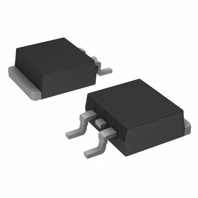
VS-8EWF06SLHM3
www.vishay.com
Vishay Semiconductors
Surface Mount Fast Soft Recovery Rectifier Diode, 8 A
FEATURES
Base
cathode
+
2
• Glass passivated pellet chip junction
• Meets MSL level 1, per J-STD-020, LF maximum
peak of 260 °C
• AEC-Q101 qualified
2
• Meets JESD 201 class 2 whisker test
3
1
DPAK (TO-252AA)
1
Anode -
3
- Anode
• Flexible solution
rectification
for
reliable
AC
power
• High surge, low VF rugged blocking diode for DC charging
stations
PRIMARY CHARACTERISTICS
IF(AV)
8A
VR
600 V
• Material categorization: for definitions of compliance
please see www.vishay.com/doc?99912
VF at IF
1.2 V
APPLICATIONS
IFSM
150 A
• On-board and off-board EV / HEV battery chargers
trr
55 ns
• Renewable energy inverters
TJ max.
150 °C
Snap factor
0.5
Package
DPAK (TO-252AA)
Circuit configuration
Single
DESCRIPTION
The VS-8EWF06SLHM3 fast soft recovery rectifier series
has been optimized for combined short reverse recovery
time, low forward voltage drop and low leakage current.
The glass passivation ensures stable reliable operation in
the most severe temperature and power cycling conditions.
MAJOR RATINGS AND CHARACTERISTICS
SYMBOL
IF(AV)
CHARACTERISTICS
VALUES
UNITS
8
A
Sinusoidal waveform
VRRM
600
V
IFSM
150
A
VF
8 A, TJ = 25 °C
1.2
V
trr
1 A, 100 A/μs
55
ns
TJ
Range
-40 to +150
°C
VRRM, MAXIMUM PEAK
REVERSE VOLTAGE
V
VRSM, MAXIMUM NON-REPETITIVE
PEAK REVERSE VOLTAGE
V
IRRM
AT 150 °C
mA
600
700
3
VOLTAGE RATINGS
PART NUMBER
VS-8EWF06SLHM3
ABSOLUTE MAXIMUM RATINGS
PARAMETER
SYMBOL
TEST CONDITIONS
VALUES
Maximum average forward current
IF(AV)
TC = 96 °C, 180° conduction half sine wave
8
Maximum peak one cycle
non-repetitive surge current
IFSM
10 ms sine pulse, rated VRRM applied
125
10 ms sine pulse, no voltage reapplied
150
Maximum I2t for fusing
I2t
Maximum I2t for fusing
I2t
10 ms sine pulse, rated VRRM applied
78
10 ms sine pulse, no voltage reapplied
110
t = 0.1 ms to 10 ms, no voltage reapplied
1100
UNITS
A
A2s
A2s
Revision: 22-Feb-18
Document Number: 96117
1
For technical questions within your region: DiodesAmericas@vishay.com, DiodesAsia@vishay.com, DiodesEurope@vishay.com
THIS DOCUMENT IS SUBJECT TO CHANGE WITHOUT NOTICE. THE PRODUCTS DESCRIBED HEREIN AND THIS DOCUMENT
ARE SUBJECT TO SPECIFIC DISCLAIMERS, SET FORTH AT www.vishay.com/doc?91000
�VS-8EWF06SLHM3
www.vishay.com
Vishay Semiconductors
ELECTRICAL SPECIFICATIONS
PARAMETER
SYMBOL
Maximum forward voltage drop
VFM
Forward slope resistance
rt
Threshold voltage
VALUES
TJ = 150 °C
VF(TO)
Maximum reverse leakage current
TEST CONDITIONS
8 A, TJ = 25 °C
TJ = 25 °C
IRM
V
16
m
1.13
V
0.1
VR = rated VRRM
TJ = 150 °C
UNITS
1.2
mA
3
RECOVERY CHARACTERISTICS
PARAMETER
SYMBOL
TEST CONDITIONS
VALUES
55
trr
IF at 1 Apk
100 A/μs
TJ = 25 °C
Reverse recovery time
Reverse recovery current
Irr
Reverse recovery charge
Qrr
Snap factor
IF at 8 Apk
25 A/μs
TJ = 25 °C
S
UNITS
ns
IFM
trr
200
ta
2.6
A
0.25
μC
tb
t
di
dt
Qrr
Irr
0.5
THERMAL - MECHANICAL SPECIFICATIONS
PARAMETER
SYMBOL
Maximum junction and storage
temperature range
TEST CONDITIONS
TJ, TStg
Maximum thermal resistance,
junction to case
RthJC
VALUES
UNITS
-40 to +150
°C
DC operation
2.5
°C/W
Typical thermal resistance,
junction to ambient (PCB mount)
RthJA (1)
50
Approximate weight
Marking device
1
g
0.03
oz.
Case style DPAK (TO-252AA)
8EWF06SH
150
140
Maximum Allowable Case Temperature (°C)
Maximum Allowable Case Temperature (°C)
Note
(1) When mounted on 1" square (650 mm2) PCB of FR-4 or G-10 material 4 oz. (140 μm) copper 40 °C/W
R thJC (DC) = 2.5 °C/W
130
120
Conduction angle
110
100
90
30°
80
60°
90°
120°
180°
70
60
0
1
2
3
4
5
6
7
8
9
Average Forward Current (A)
Fig. 1 - Current Rating Characteristics
150
R thJC (DC) = 2.5 °C/W
140
130
120
110
Conduction period
100
30°
60°
90
90°
120°
80
180°
DC
70
0
2
4
6
8
10
12
14
Average Forward Current (A)
Fig. 2 - Current Rating Characteristics
Revision: 22-Feb-18
Document Number: 96117
2
For technical questions within your region: DiodesAmericas@vishay.com, DiodesAsia@vishay.com, DiodesEurope@vishay.com
THIS DOCUMENT IS SUBJECT TO CHANGE WITHOUT NOTICE. THE PRODUCTS DESCRIBED HEREIN AND THIS DOCUMENT
ARE SUBJECT TO SPECIFIC DISCLAIMERS, SET FORTH AT www.vishay.com/doc?91000
�VS-8EWF06SLHM3
Vishay Semiconductors
12
170
Peak Half Sine Wave Forward Current (A)
Maximum Average Forward Power Loss (W)
www.vishay.com
180°
120°
90°
60°
30°
10
8
RMS Limit
6
Conduction angle
4
2
TJ = 150 °C
130
110
90
70
50
30
0
0
1
2
3
4
5
6
7
8
Maximum non-repetitive surge current
vs. pulse train duration.
Initial Tj = Tj max.
No voltage reapplied
Rated Vrrm reapplied
150
10
0.01
9
0.1
1
Pulse Train Duration (s)
Average Forward Current (A)
Fig. 6 - Maximum Non-Repetitive Surge Current
16
100
DC
180°
120°
90°
60°
30°
14
12
10
8
Instantaneous Forward Current (A)
Maximum Average Forward Power Loss (W)
Fig. 3 - Forward Power Loss Characteristics
RMS Limit
6
Conduction period
4
TJ = 150 °C
2
0
0
2
4
6
8
10
12
10
TJ = 25 °C
TJ = 150 °C
1
0.5
14
Average Forward Current (A)
120
110
100
90
80
70
60
50
40
30
1
10
100
Number of Equal Amplitude Half Cycle
Current Pulses (N)
Fig. 5 - Maximum Non-Repetitive Surge Current
2
2.5
3
0.4
Typical Reverse Recovery Time - trr (µs)
At any rated load condition and with
rated Vrrm applied following surge.
Initial Tj = 150°C
at 60 Hz 0.0083s
at 50 Hz 0.0100s
1.5
Fig. 7 - Forward Voltage Drop Characteristics
140
130
1
Instantaneous Forward Voltage (V)
Fig. 4 - Forward Power Loss Characteristics
Peak Half Sine Wave Forward Current (A)
10
TJ = 25 °C
0.3
I FM = 20 A
0.2
10 A
8A
5A
0.1
2A
1A
0
0
40
80
120
160
200
Rate Of Fall Of Forward Current - dI/dt (A/µs)
Fig. 8 - Recovery Time Characteristics, TJ = 25 °C
Revision: 22-Feb-18
Document Number: 96117
3
For technical questions within your region: DiodesAmericas@vishay.com, DiodesAsia@vishay.com, DiodesEurope@vishay.com
THIS DOCUMENT IS SUBJECT TO CHANGE WITHOUT NOTICE. THE PRODUCTS DESCRIBED HEREIN AND THIS DOCUMENT
ARE SUBJECT TO SPECIFIC DISCLAIMERS, SET FORTH AT www.vishay.com/doc?91000
�VS-8EWF06SLHM3
www.vishay.com
Vishay Semiconductors
Typical Reverse Recovery Charge - Qrr (µC)
Typical Reverse Recovery Time - trr (µs)
0.4
TJ = 150 °C
0.3
I FM = 20 A
0.2
10 A
8A
5A
0.1
2A
1A
0
0
40
80
120
160
2.4
2
1.8
10 A
1.6
8A
1.4
1.2
5A
1
0.8
2A
0.6
0.4
1A
0.2
200
0
Rate Of Fall Of Forward Current - dI/dt (A/µs)
40
80
120
160
200
Rate Of Fall Of Forward Current - dI/dt (A/µs)
Fig. 11 - Recovery Charge Characteristics, TJ = 150 °C
Fig. 9 - Recovery Time Characteristics, TJ = 150 °C
1.4
16
TJ = 25 °C
1.2
Typical Reverse Recovery Current - Irr (A)
Typical Reverse Recovery Charge - Qrr (µC)
I FM = 20 A
TJ = 150 °C
2.2
I FM = 20 A
1
10 A
0.8
8A
0.6
5A
0.4
2A
1A
0.2
0
0
40
80
120
160
14
I FM = 20 A
TJ = 25 °C
10 A
12
8A
10
5A
8
2A
6
1A
4
2
0
0
200
40
80
120
160
200
Rate Of Fall Of Forward Current - dI/dt (A/µs)
Rate Of Fall Of Forward Current - dI/dt (A/µs)
Fig. 10 - Recovery Charge Characteristics, TJ = 25 °C
Fig. 12 - Recovery Current Characteristics, TJ = 25 °C
Typical Reverse Recovery Current - Irr (A)
20
I FM = 20 A
18
TJ = 150 °C
16
10 A
14
8A
12
5A
10
2A
8
1A
6
4
2
0
0
40
80
120
160
200
Rate Of Fall Of Forward Current - dI/dt (A/µs)
Fig. 13 - Recovery Current Characteristics, TJ = 150 °C
Revision: 22-Feb-18
Document Number: 96117
4
For technical questions within your region: DiodesAmericas@vishay.com, DiodesAsia@vishay.com, DiodesEurope@vishay.com
THIS DOCUMENT IS SUBJECT TO CHANGE WITHOUT NOTICE. THE PRODUCTS DESCRIBED HEREIN AND THIS DOCUMENT
ARE SUBJECT TO SPECIFIC DISCLAIMERS, SET FORTH AT www.vishay.com/doc?91000
�VS-8EWF06SLHM3
Transient Thermal Impedance Z thJC (°C/W)
www.vishay.com
Vishay Semiconductors
10
Steady state value
(DC operation)
D = 0.50
D = 0.33
D = 0.25
D = 0.17
D = 0.08
1
Single pulse
0.1
0.0001
0.001
0.01
0.1
Square Wave Pulse Duration (s)
Fig. 14 - Thermal Impedance ZthJC Characteristics
ORDERING INFORMATION TABLE
Device code
VS-
8
E
W
F
06
S
L
H
M3
1
2
3
4
5
6
7
8
9
10
1
-
Vishay Semiconductors product
2
-
Current rating (8 = 8 A)
3
-
Circuit configuration:
E = single
4
-
Package:
W = DPAK (TO-252AA)
5
-
Type of silicon:
F = fast soft recovery rectifier
6
-
Voltage code x 100 = VRRM
7
-
S = surface mountable
8
-
L = tape and reel (left oriented), for different orientation contact factory
9
-
H = AEC-Q101 qualified
10
-
Environmental digit:
06 = 600 V
M3 = halogen-free, RoHS-compliant, and terminations lead (Pb)-free
ORDERING INFORMATION (Example)
PREFERRED P/N
VS-8EWF06SLHM3
QUANTITY PER T/R
MINIMUM ORDER QUANTITY
PACKAGING DESCRIPTION
3000
3000
13" diameter reel
LINKS TO RELATED DOCUMENTS
Dimensions
www.vishay.com/doc?95519
Part marking information
www.vishay.com/doc?95518
Packaging information
www.vishay.com/doc?96495
Revision: 22-Feb-18
Document Number: 96117
5
For technical questions within your region: DiodesAmericas@vishay.com, DiodesAsia@vishay.com, DiodesEurope@vishay.com
THIS DOCUMENT IS SUBJECT TO CHANGE WITHOUT NOTICE. THE PRODUCTS DESCRIBED HEREIN AND THIS DOCUMENT
ARE SUBJECT TO SPECIFIC DISCLAIMERS, SET FORTH AT www.vishay.com/doc?91000
�Outline Dimensions
www.vishay.com
Vishay Semiconductors
DPAK (TO-252AA)
DIMENSIONS in millimeters and inches
Pad layout
E
A
0.265 (6.74) min.
b3
E1
c2
L3
4
4
Seating
plane
D
1
2
L5
0.245 (6.23) min.
H
L4
3
D1
3
1
2
0.488 (12.40)
0.409 (10.40)
Detail “C”
b2
0.089 (2.28) min.
c
b
e
L1
e1
Lead tip
0.06 (1.524) min.
Detail “C”
Gauge plane
L2
0.093 (2.38)
0.085 (2.18)
A1
SYMBOL
MILLIMETERS
INCHES
MIN.
MAX.
MIN.
MAX.
NOTES
SYMBOL
MILLIMETERS
MIN.
MAX.
MAX.
A
2.18
2.39
0.086
0.094
e
A1
-
0.13
-
0.005
H
9.40
10.41
0.370
0.410
b
0.64
0.89
0.025
0.035
L
1.40
1.78
0.055
0.070
b2
0.76
1.14
0.030
0.045
L1
b3
4.95
5.46
0.195
0.215
c
0.46
0.61
0.018
0.024
3
0.46
0.89
0.018
0.035
D
5.97
6.22
0.235
0.245
5
D1
5.21
-
0.205
-
3
E
6.35
6.73
0.250
0.265
5
E1
4.32
-
0.170
-
3
2.74 BSC
L2
L3
c2
2.29 BSC
INCHES
MIN.
0.51 BSC
0.89
1.27
NOTES
0.090 BSC
0.108 REF.
0.020 BSC
0.035
0.050
L4
-
1.02
-
0.040
L5
1.14
1.52
0.045
0.060
3
2
Notes
(1) Dimensioning and tolerancing as per ASME Y14.5M-1994
(2) Lead dimension uncontrolled in L5
(3) Dimension D1, E1, L3 and b3 establish a minimum mounting surface for thermal pad
(4) Dimensions D and E do not include mold flash. Mold flash shall not exceed 0.127 mm (0.005") per side. These dimensions are measured at
the outermost extremes of the plastic body
(5) Outline conforms to JEDEC® outline TO-252AA
Revision: 06-Jun-17
Document Number: 95519
1
For technical questions within your region: DiodesAmericas@vishay.com, DiodesAsia@vishay.com, DiodesEurope@vishay.com
THIS DOCUMENT IS SUBJECT TO CHANGE WITHOUT NOTICE. THE PRODUCTS DESCRIBED HEREIN AND THIS DOCUMENT
ARE SUBJECT TO SPECIFIC DISCLAIMERS, SET FORTH AT www.vishay.com/doc?91000
�Legal Disclaimer Notice
www.vishay.com
Vishay
Disclaimer
ALL PRODUCT, PRODUCT SPECIFICATIONS AND DATA ARE SUBJECT TO CHANGE WITHOUT NOTICE TO IMPROVE
RELIABILITY, FUNCTION OR DESIGN OR OTHERWISE.
Vishay Intertechnology, Inc., its affiliates, agents, and employees, and all persons acting on its or their behalf (collectively,
“Vishay”), disclaim any and all liability for any errors, inaccuracies or incompleteness contained in any datasheet or in any other
disclosure relating to any product.
Vishay makes no warranty, representation or guarantee regarding the suitability of the products for any particular purpose or
the continuing production of any product. To the maximum extent permitted by applicable law, Vishay disclaims (i) any and all
liability arising out of the application or use of any product, (ii) any and all liability, including without limitation special,
consequential or incidental damages, and (iii) any and all implied warranties, including warranties of fitness for particular
purpose, non-infringement and merchantability.
Statements regarding the suitability of products for certain types of applications are based on Vishay's knowledge of typical
requirements that are often placed on Vishay products in generic applications. Such statements are not binding statements
about the suitability of products for a particular application. It is the customer's responsibility to validate that a particular product
with the properties described in the product specification is suitable for use in a particular application. Parameters provided in
datasheets and / or specifications may vary in different applications and performance may vary over time. All operating
parameters, including typical parameters, must be validated for each customer application by the customer's technical experts.
Product specifications do not expand or otherwise modify Vishay's terms and conditions of purchase, including but not limited
to the warranty expressed therein.
Hyperlinks included in this datasheet may direct users to third-party websites. These links are provided as a convenience and
for informational purposes only. Inclusion of these hyperlinks does not constitute an endorsement or an approval by Vishay of
any of the products, services or opinions of the corporation, organization or individual associated with the third-party website.
Vishay disclaims any and all liability and bears no responsibility for the accuracy, legality or content of the third-party website
or for that of subsequent links.
Except as expressly indicated in writing, Vishay products are not designed for use in medical, life-saving, or life-sustaining
applications or for any other application in which the failure of the Vishay product could result in personal injury or death.
Customers using or selling Vishay products not expressly indicated for use in such applications do so at their own risk. Please
contact authorized Vishay personnel to obtain written terms and conditions regarding products designed for such applications.
No license, express or implied, by estoppel or otherwise, to any intellectual property rights is granted by this document or by
any conduct of Vishay. Product names and markings noted herein may be trademarks of their respective owners.
© 2021 VISHAY INTERTECHNOLOGY, INC. ALL RIGHTS RESERVED
Revision: 09-Jul-2021
1
Document Number: 91000
�