VS-C40CP07L-M3
www.vishay.com
Vishay Semiconductors
650 V Power SiC Merged PIN Schottky Diode, 2 x 20 A
Base common
cathode
2
1
2
1
Anode
3
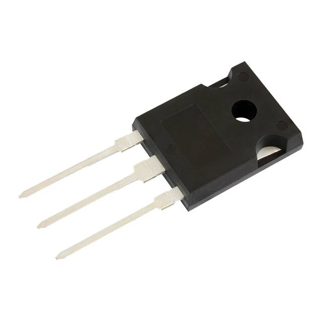
TO-247AD 3L
2
3
Anode
Common
Cathode
LINKS TO ADDITIONAL RESOURCES
3D 3D
3D Models
Models
Application
Notes
FEATURES
• Majority carrier diode using Schottky technology
on SiC wide band gap material
• Positive VF temperature coefficient, for easy
paralleling
• Virtually no recovery tail and no switching losses
• Temperature invariant switching behavior
• 175 °C maximum operating junction temperature
• MPS structure for high ruggedness to forward current
surge events
• Meets JESD 201 class 1A whisker test
• Solder Bath temperature 275 °C maximum, 10 s per
JESD 22-B106
• Material categorization: for definitions of compliance
please see www.vishay.com/doc?99912
DESCRIPTION / APPLICATIONS
PRIMARY CHARACTERISTICS
IF(AV)
Wide band gap SiC based 650 V Schottky diode, designed
for high performance and ruggedness.
Optimum choice for high speed hard switching and efficient
operation over a wide temperature range, it is also
recommended for all applications suffering from Silicon
ultrafast recovery behavior.
Typical applications include AC/DC PFC and DC/DC ultra
high frequency output rectification in FBPS and LLC
converters.
2 x 20 A
VR
650 V
VF at IF at 150 °C
1.55 V
TJ max.
175 °C
IR at VR at 175 °C
35 μA
QC (VR = 400 V)
68 nC
Package
TO-247AD 3L
Circuit configuration
Common cathode
MECHANICAL DATA
Case: TO-247AD 3L
Molding compound meets UL 94 V-0 flammability rating
Base P/N-M3 - halogen-free, RoHS-compliant
Terminals: matte tin plated leads, solderable per
J-STD-002 and JESD 22-B102
Mounting torque: 10 in-lbs maximum
ABSOLUTE MAXIMUM RATINGS (TA = 25 °C unless otherwise specified)
PARAMETER
SYMBOL
Peak repetitive reverse voltage
VRRM
Average rectified forward current, per leg
IF(AV)
DC blocking voltage
VDC
Repetitive peak surge current, per leg
IFRM
Non-repetitive peak forward surge current, per leg
IFSM
Power dissipation, per leg
Ptot (1)
I2t value, per leg
i
Operating junction and storage temperatures
2
dt
TEST CONDITIONS
TC = 140 °C (DC)
VALUES
UNITS
650
V
20
A
650
V
TC = 25 °C, f = 50 Hz, square wave, DC = 25 %
92
A
TC = 25 °C, tp = 10 ms, half sine wave
160
TC = 110 °C, tp = 10 ms, half sine wave
140
TC = 25°C
170
TC = 110 °C
74
TC = 25°C
128
TC = 110 °C
98
TJ(2), TStg
-55 to +175
A
W
A2s
°C
Notes
(1) Based on maximum R
th
(2) The heat generated must be less than the thermal conductivity from junction-to-ambient: dP /dT < 1/R
D
J
θJA
Revision: 16-Apr-2021
Document Number: 96722
1
For technical questions within your region: DiodesAmericas@vishay.com, DiodesAsia@vishay.com, DiodesEurope@vishay.com
THIS DOCUMENT IS SUBJECT TO CHANGE WITHOUT NOTICE. THE PRODUCTS DESCRIBED HEREIN AND THIS DOCUMENT
ARE SUBJECT TO SPECIFIC DISCLAIMERS, SET FORTH AT www.vishay.com/doc?91000
�VS-C40CP07L-M3
www.vishay.com
Vishay Semiconductors
ELECTRICAL SPECIFICATIONS (TJ = 25 °C unless otherwise specified)
PARAMETER
SYMBOL
Forward voltage, per leg
TEST CONDITIONS
VF
Reverse leakage current, per leg
IR
Total capacitance, per leg
C
Total capacitive charge, per leg
QC
MIN.
TYP.
MAX.
IF = 20 A
-
1.40
1.70
IF = 20 A, TJ = 150 °C
-
1.55
1.9
IF = 20 A, TJ = 175 °C
-
1.60
-
UNITS
V
VR = VR rated
-
-
100
VR = VR rated, TJ = 150 °C
-
-
250
VR = VR rated, TJ = 175 °C
-
35
-
VR = 1 V, f = 1 MHz
-
1040
-
VR = 400 V, f = 1 MHz
-
110
-
VR = 400 V, f = 1 MHz
-
68
-
nC
MIN.
TYP.
MAX.
UNITS
-
0.63
0.88
-
0.38
0.53
μA
pF
THERMAL - MECHANICAL SPECIFICATIONS (TA = 25 °C unless otherwise specified)
PARAMETER
SYMBOL
Thermal resistance, junction-to-case
per leg
TEST CONDITIONS
RthJC
per device
Marking device
C40CP07L
Axis Title
Axis Title
10000
40
10000
10000
1000
1000
100
100
30
25
1000
TJ = 25 °C
TJ = 125 °C
TJ = 150 °C
TJ = 175 °C
20
15
100
10
5
10
0
0
0.5
1.0
1.5
2.0
1st line
2nd line
35
2nd line
CT - Junction Capacitance (pF)
TJ = -55 °C
1st line
2nd line
2nd line
IF - Instantaneous Forward Current (A)
°C/W
TJ = 25 °C
f = 1.0 MHz
10
0.1
2.5
1
10
100
10
1000
VF - Forward Voltage Drop (V)
VR - Reverse Voltage (V)
Fig. 1 - Typical Forward Voltage Drop Characteristics, per leg
Fig. 3 - Typical Junction Capacitance vs. Reverse Voltage, per leg
Axis Title
Axis Title
10000
100
1000
10000
TJ = 25 °C
1000
TJ = 150 °C
TJ = 125 °C
TJ = 25 °C
TJ = -55 °C
0.01
2nd line
IFSM (A)
0.1
1000
1st line
2nd line
TJ = 175 °C
1
1st line
2nd line
2nd line
IR - Reverse Current (µA)
10
TJ = 110 °C
100
100
100
0.001
10
0.0001
0
100
200
300
400
500
600
700
10
0.0001
0.001
10
0.01
VR - Reverse Voltage (V)
tp (s)
Fig. 2 - Typical Values of Reverse Current vs. Reverse Voltage,
per leg
Fig. 4 - Non-Repetitive Peak Forward Surge Current vs.
Pulse Duration, Per Leg (Square Wave)
Revision: 16-Apr-2021
Document Number: 96722
2
For technical questions within your region: DiodesAmericas@vishay.com, DiodesAsia@vishay.com, DiodesEurope@vishay.com
THIS DOCUMENT IS SUBJECT TO CHANGE WITHOUT NOTICE. THE PRODUCTS DESCRIBED HEREIN AND THIS DOCUMENT
ARE SUBJECT TO SPECIFIC DISCLAIMERS, SET FORTH AT www.vishay.com/doc?91000
�VS-C40CP07L-M3
www.vishay.com
Vishay Semiconductors
10000
1
1000
1st line
2nd line
ZthJC - Thermal Impedance
Junction to Case (°C/W)
Axis Title
10
D = 0.5
D = 0.2
D = 0.1
D = 0.05
D = 0.02
D = 0.01
DC
0.1
0.01
0.00001
0.0001
100
10
0.001
0.01
0.1
1
10
t1 - Rectangular Pulse Duration (s)
Fig. 5 - Typical Thermal Impedance ZthJC Characteristics, per leg
Axis Title
Axis Title
10000
10000
30
170
25
1000
155
150
145
140
100
135
130
1000
20
1st line
2nd line
160
2nd line
Capacitive Energy (µJ)
165
1st line
2nd line
2nd line
Allowable Case Temperature (°C)
175
15
100
10
TJ = 25 °C
f = 1.0 MHz
5
125
10
120
0
5
10
15
20
10
0
25
0
100
200
300
400
500
600
700
IF(AV) - Average Forward Output Current (A)
Reverse Voltage (V)
Fig. 6 - Maximum Allowable Case Temperature vs.
Average Forward Current, per leg
Fig. 8 - Typical Capacitive Energy vs. Reverse Voltage, per leg
Axis Title
Axis Title
10000
250
100
10000
200
RthJC typ.
100
100
RthJC max.
50
70
1000
60
1st line
2nd line
1000
150
2nd line
Capacitive Charge (nC)
80
1st line
2nd line
2nd line
Allowable Input Power (W)
90
50
40
100
TJ = 25 °C
f = 1.0 MHz
30
20
10
10
0
25
50
75
100
125
150
175
10
0
0
100
200
300
400
500
600
700
Case Temperature (°C)
Reverse Voltage (V)
Fig. 7 - Forward Power Loss Characteristics, per leg
Fig. 9 - Typical Capacitive Charge vs. Reverse Voltage, per leg
Revision: 16-Apr-2021
Document Number: 96722
3
For technical questions within your region: DiodesAmericas@vishay.com, DiodesAsia@vishay.com, DiodesEurope@vishay.com
THIS DOCUMENT IS SUBJECT TO CHANGE WITHOUT NOTICE. THE PRODUCTS DESCRIBED HEREIN AND THIS DOCUMENT
ARE SUBJECT TO SPECIFIC DISCLAIMERS, SET FORTH AT www.vishay.com/doc?91000
�VS-C40CP07L-M3
www.vishay.com
Vishay Semiconductors
ORDERING INFORMATION TABLE
Device code
VS-
C
40
C
P
07
L
-M3
1
2
3
4
5
6
7
8
1
-
Vishay Semiconductors product
2
-
C = SiC diode
3
-
Current rating (40 = 40 A)
4
-
C = common cathode
5
-
P = package TO-247
6
-
Voltage rating: (07 = 650 V)
7
-
L = long lead
8
-
Environmental digit:
-M3 = halogen-free, RoHS-compliant, and termination lead (Pb)-free
ORDERING INFORMATION
PREFERRED P/N
BASE QUANTITY
MINIMUM ORDER QUANTITY
PACKAGING DESCRIPTION
VS-C40CP07L-M3
25/tube
500
Antistatic plastic tubes
LINKS TO RELATED DOCUMENTS
Dimensions
www.vishay.com/doc?95626
Part marking information
www.vishay.com/doc?95007
SPICE model
www.vishay.com/doc?96888
Revision: 16-Apr-2021
Document Number: 96722
4
For technical questions within your region: DiodesAmericas@vishay.com, DiodesAsia@vishay.com, DiodesEurope@vishay.com
THIS DOCUMENT IS SUBJECT TO CHANGE WITHOUT NOTICE. THE PRODUCTS DESCRIBED HEREIN AND THIS DOCUMENT
ARE SUBJECT TO SPECIFIC DISCLAIMERS, SET FORTH AT www.vishay.com/doc?91000
�Legal Disclaimer Notice
www.vishay.com
Vishay
Disclaimer
ALL PRODUCT, PRODUCT SPECIFICATIONS AND DATA ARE SUBJECT TO CHANGE WITHOUT NOTICE TO IMPROVE
RELIABILITY, FUNCTION OR DESIGN OR OTHERWISE.
Vishay Intertechnology, Inc., its affiliates, agents, and employees, and all persons acting on its or their behalf (collectively,
“Vishay”), disclaim any and all liability for any errors, inaccuracies or incompleteness contained in any datasheet or in any other
disclosure relating to any product.
Vishay makes no warranty, representation or guarantee regarding the suitability of the products for any particular purpose or
the continuing production of any product. To the maximum extent permitted by applicable law, Vishay disclaims (i) any and all
liability arising out of the application or use of any product, (ii) any and all liability, including without limitation special,
consequential or incidental damages, and (iii) any and all implied warranties, including warranties of fitness for particular
purpose, non-infringement and merchantability.
Statements regarding the suitability of products for certain types of applications are based on Vishay's knowledge of typical
requirements that are often placed on Vishay products in generic applications. Such statements are not binding statements
about the suitability of products for a particular application. It is the customer's responsibility to validate that a particular product
with the properties described in the product specification is suitable for use in a particular application. Parameters provided in
datasheets and / or specifications may vary in different applications and performance may vary over time. All operating
parameters, including typical parameters, must be validated for each customer application by the customer's technical experts.
Product specifications do not expand or otherwise modify Vishay's terms and conditions of purchase, including but not limited
to the warranty expressed therein.
Hyperlinks included in this datasheet may direct users to third-party websites. These links are provided as a convenience and
for informational purposes only. Inclusion of these hyperlinks does not constitute an endorsement or an approval by Vishay of
any of the products, services or opinions of the corporation, organization or individual associated with the third-party website.
Vishay disclaims any and all liability and bears no responsibility for the accuracy, legality or content of the third-party website
or for that of subsequent links.
Except as expressly indicated in writing, Vishay products are not designed for use in medical, life-saving, or life-sustaining
applications or for any other application in which the failure of the Vishay product could result in personal injury or death.
Customers using or selling Vishay products not expressly indicated for use in such applications do so at their own risk. Please
contact authorized Vishay personnel to obtain written terms and conditions regarding products designed for such applications.
No license, express or implied, by estoppel or otherwise, to any intellectual property rights is granted by this document or by
any conduct of Vishay. Product names and markings noted herein may be trademarks of their respective owners.
© 2021 VISHAY INTERTECHNOLOGY, INC. ALL RIGHTS RESERVED
Revision: 09-Jul-2021
1
Document Number: 91000
�