VS-E5PH7506L-N3
www.vishay.com
Vishay Semiconductors
Hyperfast Rectifier, 75 A FRED Pt® G5
FEATURES
Base cathode
• Hyperfast and optimized Qrr
2
• Best in class forward voltage drop and switching
losses trade off
2
• Optimized for high speed operation
1
• 175 °C maximum operating junction temperature
3
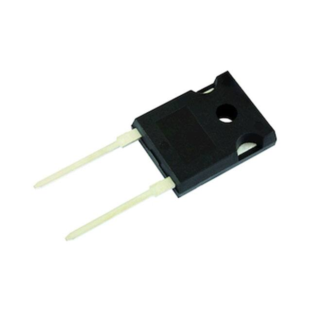
TO-247AD 2L
3
Anode
1
Cathode
• Polyimide passivation
• Material categorization: for definitions of compliance
please see www.vishay.com/doc?99912
PRIMARY CHARACTERISTICS
IF(AV)
75 A
VR
600 V
VF at IF at 125 °C
1.2 V
trr (typ.)
32
IFSM
615
TJ max.
175 °C
Package
TO-247AD 2L
Circuit configuration
Single
DESCRIPTION / APPLICATIONS
Featuring a unique combination of low conduction and
switching losses, this rectifier is the right choice for soft
switched and resonant converters, as well as medium
frequency hard switching converters. This device is
specifically designed to improve efficiency of high speed
LLC output rectification stages of EV / HEV battery charging
stations and high frequency stages of UPS applications.
ABSOLUTE MAXIMUM RATINGS
PARAMETER
SYMBOL
TEST CONDITIONS
VALUES
UNITS
600
V
Repetitive peak reverse voltage
VRRM
Average rectified forward current
IF(AV)
TC = 113 °C, D = 0.50
75
Non-repetitive peak surge current
IFSM
TC = 25 °C, tp = 10 ms, sine wave
615
Repetitive peak forward current
IFRM
TC = 113 °C, D = 0.50, f = 20 kHz
150
Operating junction and storage temperature
TJ, TStg
A
-55 to +175
°C
ELECTRICAL SPECIFICATIONS (TJ = 25 °C unless otherwise specified)
PARAMETER
Breakdown voltage, blocking voltage
SYMBOL
VBR, VR
Forward voltage
VF
Reverse leakage current
IR
Junction capacitance
CT
Series inductance
LS
TEST CONDITIONS
MIN.
TYP.
MAX.
600
-
-
IF = 75 A
-
1.3
1.7
IF = 75 A, TJ = 125 °C
-
1.2
-
IR = 100 μA
UNITS
V
VR = VR rated
-
-
25
TJ = 125 °C, VR = VR rated
-
-
500
VR = 200 V
-
96
-
pF
Measured to lead 5 mm from package body
-
8
-
nH
μA
Revision: 08-Feb-2021
Document Number: 96756
1
For technical questions within your region: DiodesAmericas@vishay.com, DiodesAsia@vishay.com, DiodesEurope@vishay.com
THIS DOCUMENT IS SUBJECT TO CHANGE WITHOUT NOTICE. THE PRODUCTS DESCRIBED HEREIN AND THIS DOCUMENT
ARE SUBJECT TO SPECIFIC DISCLAIMERS, SET FORTH AT www.vishay.com/doc?91000
�VS-E5PH7506L-N3
www.vishay.com
Vishay Semiconductors
DYNAMIC RECOVERY CHARACTERISTICS (TJ = 25 °C unless otherwise specified)
PARAMETER
SYMBOL
Reverse recovery time
trr
Peak recovery current
Qrr
Reverse recovery time
trr
Peak recovery current
IRRM
Reverse recovery charge
MIN.
TYP.
MAX.
-
32
-
TJ = 25 °C
-
52
-
TJ = 125 °C
-
82
-
-
24
-
-
51
-
TJ = 25 °C
IRRM
Reverse recovery charge
TEST CONDITIONS
IF = 1.0 A, dIF/dt = 100 A/μs, VR = 30 V
TJ = 125 °C
TJ = 25 °C
-
805
-
TJ = 125 °C
-
2515
-
TJ = 25 °C
-
57
-
TJ = 125 °C
-
90
-
-
28
-
-
58
-
TJ = 25 °C
TJ = 125 °C
Qrr
IF = 50 A
dIF/dt = 1000 A/μs
VR = 400 V
IF = 75 A
dIF/dt = 1000 A/μs
VR = 400 V
UNITS
ns
A
nC
ns
A
TJ = 25 °C
-
969
-
TJ = 125 °C
-
3090
-
MIN.
TYP.
MAX.
UNITS
-
-
0.5
°C/W
-
5.5
-
g
-
0.2
-
oz.
6
(5)
-
12
(10)
kgf · cm
(lbf · in)
-55
-
175
°C
nC
THERMAL - MECHANICAL SPECIFICATIONS
PARAMETER
SYMBOL
Thermal resistance, junction-to-case
TEST CONDITIONS
RthJC
Weight
Mounting torque
Maximum junction and storage temperature range
TJ, TStg
Case style TO-247AD 2L
1000
E5PH7506L
1000
TJ = 175 °C
IR - Reverse Current (μA)
IF - Instantaneous Forward Current (A)
Marking device
100
TJ = 175 °C
10
TJ = 125 °C
TJ = 25 °C
1
100
TJ = 125 °C
10
1
TJ = 25 °C
0.1
0.01
0.1
0
0.5
1.0
1.5
2.0
VF - Forward Voltage Drop (V)
Fig. 1 - Forward Voltage Drop Characteristics, Per Leg
100
200
300
400
500
600
VR - Reverse Voltage (V)
Fig. 2 - Typical Values of Reverse Current vs. Reverse Voltage,
Per Leg
Revision: 08-Feb-2021
Document Number: 96756
2
For technical questions within your region: DiodesAmericas@vishay.com, DiodesAsia@vishay.com, DiodesEurope@vishay.com
THIS DOCUMENT IS SUBJECT TO CHANGE WITHOUT NOTICE. THE PRODUCTS DESCRIBED HEREIN AND THIS DOCUMENT
ARE SUBJECT TO SPECIFIC DISCLAIMERS, SET FORTH AT www.vishay.com/doc?91000
�VS-E5PH7506L-N3
www.vishay.com
Allowable Solder Pad Temperature (°C)
Vishay Semiconductors
CT - Junction Capacitance (pF)
1000
100
10
0
100
200
300
400
500
600
180
170
160
150
DC
140
130
120
110
Square wave (D = 0.50)
rated VR applied
100
90
80
0
VR - Reverse Voltage (V)
10
20
30
40
50
60
70
80
IF(AV) - Average Forward Current (A)
Fig. 3 - Typical Junction Capacitance vs. Reverse Voltage, Per Leg
Fig. 4 - Maximum Allowable Case Temperature vs.
Average Forward Current, Per Leg
Average Power Loss (W)
160
140
RMS limit
120
100
D = 0.01
D = 0.05
D = 0.10
D = 0.20
D = 0.50
DC
80
60
40
20
0
0
20
40
60
80
100
120
IF(AV) - Average Forward Current (A)
Fig. 5 - Forward Power Loss Characteristics, Per Leg
ZthJC - Thermal Impedance
Junction to Case (°C/W)
1
0.1
0.50
0.20
0.10
0.05
0.02
0.01
0.01
DC
0.001
0.00001
0.0001
0.001
0.01
0.1
1
t1 - Rectangular Pulse Duration (s)
Fig. 6 - Transient Thermal Impedance, Junction to Case, Per Leg
Revision: 08-Feb-2021
Document Number: 96756
3
For technical questions within your region: DiodesAmericas@vishay.com, DiodesAsia@vishay.com, DiodesEurope@vishay.com
THIS DOCUMENT IS SUBJECT TO CHANGE WITHOUT NOTICE. THE PRODUCTS DESCRIBED HEREIN AND THIS DOCUMENT
ARE SUBJECT TO SPECIFIC DISCLAIMERS, SET FORTH AT www.vishay.com/doc?91000
�VS-E5PH7506L-N3
www.vishay.com
Vishay Semiconductors
225
350
TJ = 125°C, VR = 400 V
IF = 75 A, VR = 400 V, low dI/dt
200
300
250
IF = 150 A
150
IF = 75 A
trr (ns)
trr (ns)
175
125
100
125 °C
200
150
25 °C
100
75
In this dI/dt range curves are not dependent
from applied IF switching current, from 0.5 to
2 times IF(AV) rating
50
IF = 37.5 A
50
0
100
1000
0
20
40
60
80
100
dIF/dt (A/μs)
dIF/dt (A/μs)
Fig. 7 - Typical Reverse Recovery Time vs. dIF/dt, Per Leg
Fig. 10 - Typical Reverse Recovery Time vs. dIF/dt, Per Leg
4500
1500
In this dI/dt range curves are not dependent
from applied IF switching current, from 0.5 to
2 times IF(AV) rating
TJ = 125 °C
4000
VR = 400 V
IF = 150 A
1200
3000
IF = 75 A
2500
IF = 37.5 A
Qrr (nC)
Qrr (nC)
3500
900
125 °C
600
IF = 75 A, VR = 400 V, low dI/dt
2000
300
25 °C
1500
0
1000
1000
0
20
40
60
80
100
dIF/dt (A/μs)
dIF/dt (A/μs)
Fig. 8 - Typical Reverse Recovery Charge vs. dIF/dt, Per Leg
Fig. 11 - Typical Reverse Recovery Charge vs. dIF/dt, Per Leg
16
70
65
60
55
50
45
40
35
30
25
20
15
10
5
TJ = 125 °C
IF = 150 A
VR = 400 V
In this dI/dt range curves are not dependent
from applied IF switching current, from 0.5 to
2 times IF(AV) rating
14
12
IF = 75 A
IF = 75 A, VR = 400 V, low dI/dt
10
Irr (A)
Irr (A)
100
8
125 °C
6
IF = 37.5 A
4
25 °C
2
0
100
1000
0
20
40
60
80
100
dIF/dt (A/μs)
dIF/dt (A/μs)
Fig. 9 - Typical Reverse Recovery Current vs. dIF/dt, Per Leg
Fig. 12 - Typical Reverse Recovery Current vs. dIF/dt, Per Leg
Revision: 08-Feb-2021
Document Number: 96756
4
For technical questions within your region: DiodesAmericas@vishay.com, DiodesAsia@vishay.com, DiodesEurope@vishay.com
THIS DOCUMENT IS SUBJECT TO CHANGE WITHOUT NOTICE. THE PRODUCTS DESCRIBED HEREIN AND THIS DOCUMENT
ARE SUBJECT TO SPECIFIC DISCLAIMERS, SET FORTH AT www.vishay.com/doc?91000
�VS-E5PH7506L-N3
www.vishay.com
Vishay Semiconductors
(3)
trr
ta
IF
tb
t0
t10 %
0
0.1 IRRM
(2)
Qrr (4)
IRRM
di(rec)M/dt (5)
(1) diF/dt
Fig. 13 - Reverse Recovery Waveform and Definitions
Notes
diF/dt - rate of change of current through zero crossing
IRRM - peak reverse recovery current
trr - reverse recovery time measured from t0, crossing point of negative going IF, to point t10%, 0.1 IRRM
(4) Q - area under curve defined by t and t
rr
0
10 %
(1)
(2)
(3)
t 10 %
Q rr =
I ( t ) dt
t0
(5)
di(rec)M/dt - peak rate of change of current during tb portion of trr
ORDERING INFORMATION TABLE
Device code
VS-
E
5
P
H
75
06
L
-N3
1
2
3
4
5
6
7
8
9
1
-
Vishay Semiconductors product
2
-
E = single diode
3
-
5 = Fred generation 5
4
-
5
-
Package:
P = TO-247 package
H = hyperfast recovery
6
-
Current rating (75 = 75 A)
7
-
Voltage rating (06 = 600 V)
8
-
Package: L = long lead (TO-247AD)
9
-
Environmental digit:
-N3 = halogen-free, RoHS-compliant, and totally lead (Pb)-free
ORDERING INFORMATION (Example)
PREFERRED P/N
QUANTITY PER TUBE
MINIMUM ORDER QUANTITY
PACKAGING DESCRIPTION
VS-E5PH7506L-N3
25
500
Antistatic plastic tube
LINKS TO RELATED DOCUMENTS
Dimensions
www.vishay.com/doc?95536
Part marking information
www.vishay.com/doc?95648
Revision: 08-Feb-2021
Document Number: 96756
5
For technical questions within your region: DiodesAmericas@vishay.com, DiodesAsia@vishay.com, DiodesEurope@vishay.com
THIS DOCUMENT IS SUBJECT TO CHANGE WITHOUT NOTICE. THE PRODUCTS DESCRIBED HEREIN AND THIS DOCUMENT
ARE SUBJECT TO SPECIFIC DISCLAIMERS, SET FORTH AT www.vishay.com/doc?91000
�Outline Dimensions
www.vishay.com
Vishay Semiconductors
TO-247AD 2L
DIMENSIONS in millimeters and inches
A
A
(3)
(6) F P
E
B
(2) R/2
A2
S
(Datum B)
Ø K M D BM
F P1
A
D2
Q
2xR
(2)
D1 (4)
D
1, 2
4
D
3
Thermal pad
(5) L1
C
L
See view B
(4)
E1
A
0.01 M D B M
View A - A
C
2 x b2
2xb
2x e
A1
0.10 M C A M
(b1, b3)
Plating
Base metal
D D
(c)
c1
C
C
(b, b2)
(4)
Section C - C, D - D
SYMBOL
MILLIMETERS
View B
INCHES
MIN.
MAX.
MIN.
MAX.
A
4.65
5.31
0.183
0.209
A1
2.21
2.59
0.087
0.102
NOTES
SYMBOL
MILLIMETERS
INCHES
MIN.
MAX.
MIN.
MAX.
E
15.29
15.87
0.602
0.625
E1
13.46
-
0.53
-
A2
1.50
2.49
0.059
0.098
e
5.46 BSC
b
0.99
1.40
0.039
0.055
ØK
0.254
b1
0.99
1.35
0.039
0.053
L
19.81
20.32
0.780
0.800
b2
1.65
2.39
0.065
0.094
L1
3.71
4.29
0.146
0.169
b3
1.65
2.34
0.065
0.092
ØP
3.56
3.66
0.14
0.144
c
0.38
0.89
0.015
0.035
Ø P1
-
6.98
-
0.275
NOTES
3
0.215 BSC
0.010
c1
0.38
0.84
0.015
0.033
Q
5.31
5.69
0.209
0.224
D
19.71
20.70
0.776
0.815
3
R
4.52
5.49
0.178
0.216
D1
13.08
-
0.515
-
4
S
D2
0.51
1.35
0.020
0.053
5.51 BSC
0.217 BSC
Notes
(1) Dimensioning and tolerancing per ASME Y14.5M-1994
(2) Contour of slot optional
(3) Dimension D and E do not include mold flash. These dimensions are measured at the outermost extremes of the plastic body
(4) Thermal pad contour optional with dimensions D1 and E1
(5) Lead finish uncontrolled in L1
(6) Ø P to have a maximum draft angle of 1.5 to the top of the part with a maximum hole diameter of 3.91 mm (0.154")
(7) Outline conforms to JEDEC® outline TO-247 with exception of dimension A min., D, E min., Q min., S, and note 4
Revision: 28-May-2018
Document Number: 95536
1
For technical questions within your region: DiodesAmericas@vishay.com, DiodesAsia@vishay.com, DiodesEurope@vishay.com
THIS DOCUMENT IS SUBJECT TO CHANGE WITHOUT NOTICE. THE PRODUCTS DESCRIBED HEREIN AND THIS DOCUMENT
ARE SUBJECT TO SPECIFIC DISCLAIMERS, SET FORTH AT www.vishay.com/doc?91000
�Legal Disclaimer Notice
www.vishay.com
Vishay
Disclaimer
ALL PRODUCT, PRODUCT SPECIFICATIONS AND DATA ARE SUBJECT TO CHANGE WITHOUT NOTICE TO IMPROVE
RELIABILITY, FUNCTION OR DESIGN OR OTHERWISE.
Vishay Intertechnology, Inc., its affiliates, agents, and employees, and all persons acting on its or their behalf (collectively,
“Vishay”), disclaim any and all liability for any errors, inaccuracies or incompleteness contained in any datasheet or in any other
disclosure relating to any product.
Vishay makes no warranty, representation or guarantee regarding the suitability of the products for any particular purpose or
the continuing production of any product. To the maximum extent permitted by applicable law, Vishay disclaims (i) any and all
liability arising out of the application or use of any product, (ii) any and all liability, including without limitation special,
consequential or incidental damages, and (iii) any and all implied warranties, including warranties of fitness for particular
purpose, non-infringement and merchantability.
Statements regarding the suitability of products for certain types of applications are based on Vishay's knowledge of typical
requirements that are often placed on Vishay products in generic applications. Such statements are not binding statements
about the suitability of products for a particular application. It is the customer's responsibility to validate that a particular product
with the properties described in the product specification is suitable for use in a particular application. Parameters provided in
datasheets and / or specifications may vary in different applications and performance may vary over time. All operating
parameters, including typical parameters, must be validated for each customer application by the customer's technical experts.
Product specifications do not expand or otherwise modify Vishay's terms and conditions of purchase, including but not limited
to the warranty expressed therein.
Hyperlinks included in this datasheet may direct users to third-party websites. These links are provided as a convenience and
for informational purposes only. Inclusion of these hyperlinks does not constitute an endorsement or an approval by Vishay of
any of the products, services or opinions of the corporation, organization or individual associated with the third-party website.
Vishay disclaims any and all liability and bears no responsibility for the accuracy, legality or content of the third-party website
or for that of subsequent links.
Except as expressly indicated in writing, Vishay products are not designed for use in medical, life-saving, or life-sustaining
applications or for any other application in which the failure of the Vishay product could result in personal injury or death.
Customers using or selling Vishay products not expressly indicated for use in such applications do so at their own risk. Please
contact authorized Vishay personnel to obtain written terms and conditions regarding products designed for such applications.
No license, express or implied, by estoppel or otherwise, to any intellectual property rights is granted by this document or by
any conduct of Vishay. Product names and markings noted herein may be trademarks of their respective owners.
© 2021 VISHAY INTERTECHNOLOGY, INC. ALL RIGHTS RESERVED
Revision: 09-Jul-2021
1
Document Number: 91000
�