VS-ETF075Y60U
www.vishay.com
Vishay Semiconductors
EMIPAK 2B PressFit Power Module
3-Levels Half Bridge Inverter Stage, 75 A
FEATURES
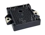
EMIPAK 2B
(package example)
PRIMARY CHARACTERISTICS
Q1 - Q4 IGBT STAGE
VCES
600 V
1.7 V
VCE(on) typical at IC = 75 A
IC at TC = 80 °C
75 A
Q2 - Q3 IGBT STAGE
600 V
VCES
VCE(on) typical at IC = 75 A
1.56 V
IC at TC = 122 °C
75 A
Speed
8 kHz to 30 kHz
Package
EMIPAK 2B
Circuit configuration
3-levels half bridge inverter stage
•
•
•
•
•
•
•
•
•
•
•
•
Trench IGBT technology
FRED Pt® clamping diodes
PressFit pins technology
Exposed Al2O3 substrate with low thermal resistance
Short circuit rated
Square RBSOA
Integrated thermistor
Low internal inductances
Low switching loss
PressFit pins locking technology. Patent # US.263.820 B2
UL approved file E78996
Material categorization: for definitions of compliance
please see www.vishay.com/doc?99912
DESCRIPTION
VS-ETF075Y60U is an integrated solution for a multi level
inverter stage in a single package. The EMIPAK2B package
is easy to use thanks to the PressFit pins and the exposed
substrate provides improved thermal performance. The
optimized layout also helps to minimize stray parameters,
allowing for better EMI performance.
ABSOLUTE MAXIMUM RATINGS
PARAMETER
Operating junction temperature
Storage temperature range
RMS isolation voltage
Q1 - Q4 IGBT
Collector to emitter voltage
Gate to emitter voltage
Pulsed collector current
Clamped inductive load current
SYMBOL
TJ
TStg
VISOL
TJ = 25 °C, all terminals shorted, f = 50 Hz, t = 1 s
IC
Power dissipation
PD
TC = 25 °C
TC = 80 °C
TSINK = 80 °C
TC = 25 °C
TC = 80 °C
TC = 25 °C
TC = 80 °C
TSINK = 80 °C
TC = 25 °C
TC = 80 °C
600
20
250
250
154
113
50
405
257
VCES
VGES
ICM
ILM (1)
Continuous collector current
IC
Power dissipation
PD
MAX.
175
-40 to +150
3500
600
20
200
200
100
75
40
294
186
VCES
VGES
ICM
ILM (1)
Continuous collector current
Q2 - Q3 IGBT
Collector to emitter voltage
Gate to emitter voltage
Pulsed collector current
Clamped inductive load current
TEST CONDITIONS
UNITS
°C
V
V
A
A
W
V
A
A
W
PATENT(S): www.vishay.com/patents
This Vishay product is protected by one or more United States and International patents.
Revision: 30-May-2022
Document Number: 94685
1
For technical questions within your region: DiodesAmericas@vishay.com, DiodesAsia@vishay.com, DiodesEurope@vishay.com
THIS DOCUMENT IS SUBJECT TO CHANGE WITHOUT NOTICE. THE PRODUCTS DESCRIBED HEREIN AND THIS DOCUMENT
ARE SUBJECT TO SPECIFIC DISCLAIMERS, SET FORTH AT www.vishay.com/doc?91000
�VS-ETF075Y60U
www.vishay.com
Vishay Semiconductors
ABSOLUTE MAXIMUM RATINGS
PARAMETER
D5 - D6 CLAMPING DIODE
SYMBOL
Repetitive peak reverse voltage
VRRM
Single pulse forward current
IFSM
Diode continuous forward current
Power dissipation
IF
PD
TEST CONDITIONS
MAX.
UNITS
600
V
10 ms sine or 6 ms rectangular pulse, TJ = 25 °C
270
TC = 25 °C
78
TC = 80 °C
55
TSINK = 80 °C
28
TC = 25 °C
174
TC = 80 °C
110
10 ms sine or 6 ms rectangular pulse, TJ = 25 °C
250
TC = 25 °C
72
TC = 80 °C
70
A
W
D1 - D2 - D3 - D4 AP DIODE
Single pulse forward current
Diode continuous forward current
Power dissipation
IFSM
IF
PD
TSINK = 80 °C
31
TC = 25 °C
107
TC = 80 °C
68
A
W
Notes
• Absolute Maximum Ratings indicate sustained limits beyond which damage to the device may occur
(1) V
CC = 300 V, VGE = 15 V, L = 500 μH, Rg = 4.7 Ω, TJ = 175 °C
ELECTRICAL SPECIFICATIONS (TJ = 25 °C unless otherwise noted)
PARAMETER
SYMBOL
TEST CONDITIONS
MIN.
TYP.
MAX.
UNITS
V
Q1 - Q4 IGBT
Collector to emitter breakdown voltage
BVCES
VGE = 0 V, IC = 100 μA
VGE = 15 V, IC = 60 A
Collector to emitter voltage
Gate threshold voltage
Temperature coefficient of threshold
voltage
VCE(on)
VGE(th)
ΔVGE(th)/ΔTJ
600
-
-
-
1.57
1.95
2.15
VGE = 15 V, IC = 75 A
-
1.7
VGE = 15 V, IC = 60 A, TJ = 125 °C
-
1.7
-
VGE = 15 V, IC = 75 A, TJ = 125 °C
-
1.86
-
3.6
5.6
7.1
-
-12
-
mV/°C
VCE = VGE, IC = 2.1 mA
VCE = VGE, IC = 1 mA (25 °C to 125 °C)
V
Forward transconductance
gfe
VCE = 20 V, IC = 75 A
-
51
-
S
Transfer characteristics
VGE
VCE = 20 V, IC = 75 A
-
9.6
-
V
VGE = 0 V, VCE = 600 V
-
0.0002
0.1
VGE = 0 V, VCE = 600 V, TJ = 125 °C
-
0.01
-
Zero gate voltage collector current
ICES
Gate to emitter leakage current
IGES
VGE = ± 20 V, VCE = 0 V
-
-
± 200
nA
BVCES
VGE = 0 V, IC = 500 μA
600
-
-
V
mA
Q2 - Q3 IGBT
Collector to emitter breakdown voltage
Collector to emitter voltage
Gate threshold voltage
Temperature coefficient of threshold
voltage
VCE(on)
VGE(th)
ΔVGE(th)/ΔTJ
VGE = 15 V, IC = 60 A
-
1.45
1.62
VGE = 15 V, IC = 75 A
-
1.56
1.73
VGE = 15 V, IC = 60 A, TJ = 125 °C
-
1.52
-
VGE = 15 V, IC = 75 A, TJ = 125 °C
-
1.67
-
3.6
5.3
7.1
-
-18
-
mV/°C
VCE = VGE, IC = 5.6 mA
VCE = VGE, IC = 1.4 mA (25 °C to 125 °C)
V
Forward transconductance
gfe
VCE = 20 V, IC = 75 A
-
72
-
S
Transfer characteristics
VGE
VCE = 20 V, IC = 75 A
-
8.3
-
V
VGE = 0 V, VCE = 600 V
-
0.0005
0.1
VGE = 0 V, VCE = 600 V, TJ = 125 °C
-
0.065
-
VGE = ± 20 V, VCE = 0 V
-
-
± 400
Zero gate voltage collector current
ICES
Gate to emitter leakage current
IGES
mA
nA
Revision: 30-May-2022
Document Number: 94685
2
For technical questions within your region: DiodesAmericas@vishay.com, DiodesAsia@vishay.com, DiodesEurope@vishay.com
THIS DOCUMENT IS SUBJECT TO CHANGE WITHOUT NOTICE. THE PRODUCTS DESCRIBED HEREIN AND THIS DOCUMENT
ARE SUBJECT TO SPECIFIC DISCLAIMERS, SET FORTH AT www.vishay.com/doc?91000
�VS-ETF075Y60U
www.vishay.com
Vishay Semiconductors
ELECTRICAL SPECIFICATIONS (TJ = 25 °C unless otherwise noted)
PARAMETER
SYMBOL
TEST CONDITIONS
MIN.
TYP.
MAX.
UNITS
D5 - D6 CLAMPING DIODE
Cathode to anode blocking voltage
VBR
Forward voltage drop
VFM
Reverse leakage current
IRM
IR = 100 μA
600
-
-
IF = 40 A
-
1.83
2.35
IF = 40 A, TJ = 125 °C
-
1.51
-
VR = 600 V
-
0.0002
0.1
VR = 600 V, TJ = 125 °C
-
0.028
-
IF = 30 A
-
1.2
1.41
IF = 30 A, TJ = 125 °C
-
1.06
-
MIN.
TYP.
MAX.
-
150
-
-
40
-
-
60
-
-
0.94
-
V
mA
D1 - D2 - D3 - D4 AP DIODE
Forward voltage drop
VFM
V
SWITCHING CHARACTERISTICS (TJ = 25 °C unless otherwise noted)
PARAMETER
SYMBOL
TEST CONDITIONS
UNITS
Q1 - Q4 IGBT (WITH D5 - D6 CLAMPING DIODE)
Total gate charge (turn-on)
Qg
Gate to emitter charge (turn-on)
Qge
Gate to collector charge (turn-on)
Qgc
Turn-on switching loss
Eon
Turn-off switching loss
Eoff
Total switching loss
Etot
Turn-on delay time
td(on)
Rise time
Turn-off delay time
Fall time
tr
td(off)
IC = 75 A
VCC = 400 V
VGE = 15 V
IC = 75 A
VCC = 300 V
VGE = 15 V
Rg = 4.7 Ω
L = 500 μH (1)
-
1.1
-
-
2.04
-
-
78
-
-
72
-
-
101
-
tf
-
65
-
Turn-on switching loss
Eon
-
1.13
-
Turn-off switching loss
Eoff
IC = 75 A
VCC = 300 V
VGE = 15 V
Rg = 4.7 Ω
L = 500 μH
TJ = 125 °C (1)
-
1.61
-
-
2.74
-
-
78
-
VGE = 0 V
VCC = 30 V
f = 1 MHz
Total switching loss
Etot
Turn-on delay time
td(on)
Rise time
Turn-off delay time
Fall time
tr
td(off)
-
72
-
-
106
-
tf
-
107
Input capacitance
Cies
-
4440
Output capacitance
Coes
-
245
Reverse transfer capacitance
Cres
-
130
Reverse bias safe operating area
RBSOA
TJ = 175 °C, IC = 200 A,VCC = 300 V,
VP = 600 V, Rg = 4.7 Ω, VGE = 15 V to 0 V
Short circuit safe operating area
SCSOA
Rg = 10 Ω, VCC = 400 V, VP = 600 V
VGE = 15 V to 0
nC
mJ
ns
mJ
ns
pF
Fullsquare
-
-
5
-
240
-
-
69
-
-
90
-
μs
Q2 - Q3 IGBT (WITH FREEWHEELING EXTERNAL TO-247 DIODE DISCRETE 30ETH06)
Total gate charge (turn-on)
Qg
Gate to emitter charge (turn-on)
Qge
Gate to collector charge (turn-on)
Qgc
IC = 120 A
VCC = 400 V
VGE = 15 V
Turn-on switching loss
Eon
-
0.85
-
Turn-off switching loss
Eoff
IC = 75 A
-
1.54
-
Total switching loss
Etot
VCC = 300 V
-
2.39
-
Turn-on delay time
td(on)
VGE = 15 V
Rg = 4.7 Ω
L = 500 μH (1)
-
111
-
-
81
-
-
130
-
-
74
-
Rise time
Turn-off delay time
Fall time
tr
td(off)
tf
nC
mJ
ns
Revision: 30-May-2022
Document Number: 94685
3
For technical questions within your region: DiodesAmericas@vishay.com, DiodesAsia@vishay.com, DiodesEurope@vishay.com
THIS DOCUMENT IS SUBJECT TO CHANGE WITHOUT NOTICE. THE PRODUCTS DESCRIBED HEREIN AND THIS DOCUMENT
ARE SUBJECT TO SPECIFIC DISCLAIMERS, SET FORTH AT www.vishay.com/doc?91000
�VS-ETF075Y60U
www.vishay.com
Vishay Semiconductors
SWITCHING CHARACTERISTICS (TJ = 25 °C unless otherwise noted)
PARAMETER
SYMBOL
Turn-on switching loss
Eon
Turn-off switching loss
Eoff
Total switching loss
Etot
Turn-on delay time
td(on)
Rise time
Turn-off delay time
Fall time
tr
td(off)
TEST CONDITIONS
MIN.
TYP.
MAX.
-
1.0
-
IC = 75 A
VCC = 300 V
VGE = 15 V
Rg = 4.7 Ω
L = 500 μH
TJ = 125 °C (1)
-
1.83
-
-
2.83
-
-
111
-
-
83
-
-
140
-
VGE = 0 V
VCC = 30 V
f = 1 MHz
tf
-
104
-
Input capacitance
Cies
-
7750
-
Output capacitance
Coes
-
550
-
Reverse transfer capacitance
Cres
-
225
-
Reverse bias safe operating area
RBSOA
TJ = 175 °C, IC = 250 A, VCC = 300 V,
VP = 600 V, Rg = 4.7 Ω, VGE = 15 V to 0 V
Short circuit safe operating area
SCSOA
Rg = 10 Ω, VCC = 400 V, VP = 600 V
VGE = 15 V to 0
UNITS
mJ
ns
pF
Fullsquare
-
-
5
μs
ns
D5 - D6 CLAMPING DIODE
Diode reverse recovery time
trr
Diode peak reverse current
Irr
Diode recovery charge
Qrr
Diode reverse recovery time
trr
Diode peak reverse current
Irr
Diode recovery charge
Qrr
VR = 200 V
IF = 50 A
dl/dt = 500 A/μs
-
59
-
-
8.5
-
A
-
257
-
nC
VR = 200 V
IF = 50 A
dl/dt = 500 A/μs, TJ = 125 °C
-
110
-
ns
-
18.5
-
A
-
1020
-
nC
VR = 200 V
IF = 50 A
dl/dt = 500 A/μs
-
108
-
ns
-
19.5
-
A
-
1062
-
nC
VR = 200 V
IF = 50 A
dl/dt = 500 A/μs, TJ = 125 °C
-
174
-
ns
-
31
-
A
-
2716
-
nC
D1 - D2 - D3 - D4 AP DIODE
Diode reverse recovery time
trr
Diode peak reverse current
Irr
Diode recovery charge
Qrr
Diode reverse recovery time
trr
Diode peak reverse current
Irr
Diode recovery charge
Qrr
Note
(1) Energy losses include “tail” and diode reverse recovery
INTERNAL NTC - THERMISTOR SPECIFICATIONS
PARAMETER
SYMBOL
TEST CONDITIONS
VALUE
UNITS
R25
TC = 25 °C
5000
R100
TC = 100 °C
493 ± 5 %
B25/50
R2 = R25 exp. [B25/50 (1/T2 - 1/(298.15 K))]
3375 ± 5 %
K
220
°C
Dissipation constant
2
mW/°C
Thermal time constant
8
s
Resistance
B-value
Maximum operating temperature
Ω
Revision: 30-May-2022
Document Number: 94685
4
For technical questions within your region: DiodesAmericas@vishay.com, DiodesAsia@vishay.com, DiodesEurope@vishay.com
THIS DOCUMENT IS SUBJECT TO CHANGE WITHOUT NOTICE. THE PRODUCTS DESCRIBED HEREIN AND THIS DOCUMENT
ARE SUBJECT TO SPECIFIC DISCLAIMERS, SET FORTH AT www.vishay.com/doc?91000
�VS-ETF075Y60U
www.vishay.com
Vishay Semiconductors
THERMAL AND MECHANICAL SPECIFICATIONS
PARAMETER
SYMBOL
MIN.
TYP.
MAX.
-
-
0.51
-
-
0.37
-
-
0.86
D1 - D2 - D3 - D4 AP diode - junction to case thermal resistance (per diode)
-
-
1.4
Q1 - Q4 IGBT - case to sink thermal resistance (per switch)
-
0.84
-
Q1 - Q4 IGBT - junction to case thermal resistance (per switch)
Q2 - Q3 IGBT - junction to case thermal resistance (per switch)
RthJC
D5 - D6 clamping diode - junction to case thermal resistance (per diode)
Q2 - Q3 IGBT - case to sink thermal resistance (per switch)
UNITS
°C/W
-
0.8
-
-
1.16
-
D1 - D2 - D3 - D4 AP diode - case to sink thermal resistance (per diode)
-
1.12
-
Case to sink thermal resistance per module
-
0.1
-
°C/W
Mounting torque (M4)
2
-
3
Nm
Weight
-
45
-
g
RthCS (1)
D5 - D6 clamping diode - case to sink thermal resistance (per diode)
Note
(1) Mounting surface flat, smooth, and greased
180
Allowable Case Temperature (°C)
150
TJ = 25 °C
135
120
105
TJ = 125 °C
TJ = 150 °C
TJ = 175 °C
IC (A)
90
75
60
45
30
15
0
0
0.5
1
1.5
2
2.5
3
3.5
160
140
120
DC
100
80
60
40
20
0
0
20
40
60
80
100
120
VCE (V)
IC - Continuous Collector Current (A)
Fig. 1 - Typical Q1 - Q4 Trench IGBT Output Characteristics
VGE = 15 V
Fig. 3 - Maximum Q1 - Q4 Trench IGBT Continuous Collector
Current vs. Case Temperature
150
80
135
70
VCE = 20 V
120
60
105
75
IC (A)
IC (A)
50
VGE = 18 V
VGE = 15 V
VGE = 12 V
90
60
40
TJ = 125 °C
30
45
30
TJ = 25 °C
20
VGE = 9 V
10
15
0
0
0
0.5
1
1.5
2
2.5
3
3.5
4
5
6
7
8
9
10
11
12
VCE (V)
VGE (V)
Fig. 2 - Typical Q1 - Q4 Trench IGBT Output Characteristics
TJ = 125 °C
Fig. 4 - Typical Q1 - Q4 Trench IGBT Transfer Characteristics
Revision: 30-May-2022
Document Number: 94685
5
For technical questions within your region: DiodesAmericas@vishay.com, DiodesAsia@vishay.com, DiodesEurope@vishay.com
THIS DOCUMENT IS SUBJECT TO CHANGE WITHOUT NOTICE. THE PRODUCTS DESCRIBED HEREIN AND THIS DOCUMENT
ARE SUBJECT TO SPECIFIC DISCLAIMERS, SET FORTH AT www.vishay.com/doc?91000
�VS-ETF075Y60U
www.vishay.com
Vishay Semiconductors
6.5
1000
6
Switching time (ns)
TJ = 25 °C
5.5
VGEth (V)
5
TJ = 125 °C
4.5
4
tf
tdoff
100
tdon
3.5
tr
3
10
0.2
0.4
0.6
0.8
1
1.2
1.4
0
1.6
10
20
30
40
50
60
70
80
IC (mA)
IC (A)
Fig. 5 - Typical Q1 - Q4 Trench IGBT Gate Threshold Voltage
Fig. 8 - Typical Q1 - Q4 Trench IGBT Switching Loss vs. IC
(with D5 - D6 Clamping Diode)
TJ = 125 °C, VCC = 300 V, Rg = 4.7 Ω, VGE = 15 V, L = 500 μH
10
2.4
1
TJ = 175 °C
0.1
TJ = 150 °C
2.2
Energy (mJ)
ICES (mA)
2
TJ = 125 °C
0.01
0.001
TJ = 25 °C
1.8
Eoff
1.6
1.4
Eon
1.2
0.0001
1
0.8
0.00001
100
200
300
400
500
600
0
5
10
15
20
25
30
35
40
45
50
VCES (V)
Rg (Ω)
Fig. 6 - Typical Q1 - Q4 Trench IGBT Zero Gate Voltage
Collector Current
Fig. 9 - Typical Q1 - Q4 Trench IGBT Energy Loss vs. Rg
(with D5 - D6 Clamping Diode)
TJ = 125 °C, VCC = 300 V, IC = 75 A, VGE = 15 V, L = 500 μH
1000
2
1.8
tdon
Switching time (ns)
1.6
Energy (mJ)
1.4
Eoff
1.2
1
0.8
Eon
0.6
0.4
tdoff
100
tf
tr
0.2
0
10
0
10
20
30
40
50
60
70
80
0
5
10
15
20
25
30
35
40
45
50
IC (A)
Rg (Ω)
Fig. 7 - Typical Q1 - Q4 Trench IGBT Energy Loss vs. IC
(with D5 - D6 Clamping Diode)
TJ = 125 °C, VCC = 300 V, Rg = 4.7 Ω, VGE = 15 V, L = 500 μH
Fig. 10 - Typical Q1 - Q4 Trench IGBT Switching Time vs. Rg
(with D5 - D6 Clamping Diode)
TJ = 125 °C, VCC = 300 V, IC = 75 A, VGE = 15 V, L = 500 μH
Revision: 30-May-2022
Document Number: 94685
6
For technical questions within your region: DiodesAmericas@vishay.com, DiodesAsia@vishay.com, DiodesEurope@vishay.com
THIS DOCUMENT IS SUBJECT TO CHANGE WITHOUT NOTICE. THE PRODUCTS DESCRIBED HEREIN AND THIS DOCUMENT
ARE SUBJECT TO SPECIFIC DISCLAIMERS, SET FORTH AT www.vishay.com/doc?91000
�VS-ETF075Y60U
www.vishay.com
Vishay Semiconductors
170
150
135
150
TJ = 175 °C
120
130
TJ = 150 °C
105
125 °C
trr (ns)
IF (A)
90
75
60
TJ = 25 °C
45
TJ = 125 °C
110
90
70
30
25 °C
50
15
30
0
0
0.5
1
1.5
2
2.5
3
3.5
100
200
VFM (V)
400
500
dIFdt (A/µs)
Fig. 14 - Typical D5 - D6 Clamping Diode
Reverse Recovery Time vs. dIF/dt, VRR = 200 V, IF = 50 A
Fig. 11 - Typical D5 - D6 Clamping Diode Forward Characteristics
180
22
160
20
125 °C
18
140
16
120
14
IRR (A)
Allowable Case Temperature (°C)
300
100
80
12
10
25 °C
8
60
6
40
4
20
2
0
0
0
10
20
30
40
50
60
70
80
100
90
200
300
400
500
IF - Continuous Forward Current (A)
dIFdt (A/µs)
Fig. 12 - Maximum D5 - D6 Clamping Diode Forward Current vs.
Case Temperature
Fig. 15 - Typical D5 - D6 Clamping Diode
Reverse Recovery Current vs. dIF/dt,
VRR = 200 V, IF = 50 A
10
1200
175 °C
1
125 °C
1000
150 °C
125 °C
0.01
800
Qrr (nC)
IRRM (A)
0.1
600
400
0.001
25 °C
0.00001
100
25 °C
200
0.0001
0
200
300
400
500
600
100
200
300
400
500
VR (V)
dIFdt (A/µs)
Fig. 13 - Typical D5 - D6 Clamping diode Reverse Leakage Current
Fig. 16 - Typical D5 - D6 Clamping Diode
Reverse Recovery Charge vs. dIF/dt,
VRR = 200 V, IF = 50 A
Revision: 30-May-2022
Document Number: 94685
7
For technical questions within your region: DiodesAmericas@vishay.com, DiodesAsia@vishay.com, DiodesEurope@vishay.com
THIS DOCUMENT IS SUBJECT TO CHANGE WITHOUT NOTICE. THE PRODUCTS DESCRIBED HEREIN AND THIS DOCUMENT
ARE SUBJECT TO SPECIFIC DISCLAIMERS, SET FORTH AT www.vishay.com/doc?91000
�VS-ETF075Y60U
www.vishay.com
Vishay Semiconductors
ZthJC - Thermal Impedance
Junction to Case (°C/W)
10
1
0.1
0.5
0.2
0.1
0.05
0.02
0.01
DC
0.01
0.001
0.00001
0.0001
0.001
0.01
0.1
1
10
t1 - Rectangular Pulse Duration (s)
Fig. 17 - Maximum Thermal Impedance ZthJC Characteristics (Q1 - Q4 Trench IGBT)
ZthJC - Thermal Impedance
Junction to Case (°C/W)
10
1
0.1
0.5
0.2
0.1
0.05
0.02
0.01
DC
0.01
0.001
0.00001
0.0001
0.001
0.01
0.1
1
10
t1 - Rectangular Pulse Duration (s)
Fig. 18 - Maximum Thermal Impedance ZthJC Characteristics (D5 - D6 Clamping Diode)
150
150
TJ = 25 °C
135
135
120
105
IC (A)
90
IC (A)
TJ = 125 °C
TJ = 150 °C
TJ = 175 °C
75
120
VGE = 18 V
VGE = 15 V
105
VGE = 12 V
90
VGE = 9 V
75
60
60
45
45
30
30
15
15
0
0
0
0.5
1
1.5
2
2.5
3
VCE (V)
Fig. 19 - Typical Q2 - Q3 Trench IGBT Output Characteristics,
VGE = 15 V
0
0.5
1
1.5
2
2.5
3
VCE (V)
Fig. 20 - Typical Q2 - Q3 Trench IGBT Output Characteristics,
TJ = 125 °C
Revision: 30-May-2022
Document Number: 94685
8
For technical questions within your region: DiodesAmericas@vishay.com, DiodesAsia@vishay.com, DiodesEurope@vishay.com
THIS DOCUMENT IS SUBJECT TO CHANGE WITHOUT NOTICE. THE PRODUCTS DESCRIBED HEREIN AND THIS DOCUMENT
ARE SUBJECT TO SPECIFIC DISCLAIMERS, SET FORTH AT www.vishay.com/doc?91000
�VS-ETF075Y60U
Vishay Semiconductors
10
180
TJ = 175 °C
160
1
120
TJ = 125 °C
0.1
DC
100
80
60
0.01
0.001
TJ = 25 °C
40
0.0001
20
0
0
20
40
60
80
100
120
140
0.00001
100
160
200
300
400
500
600
IC - Continuous Collector Current (A)
VCES (V)
Fig. 21 - Maximum Q2 - Q3 Trench IGBT
Continuous Collector Current vs. Case Temperature
Fig. 24 - Typical Q2 - Q3 Trench IGBT
Zero Gate Voltage Collector Current
80
2
VCE = 20 V
1.8
70
1.6
60
TJ = 125 °C
1.4
50
Energy (mJ)
ICE (A)
TJ = 150 °C
140
ICES (mA)
Allowable Case Temperature (°C)
www.vishay.com
TJ = 25 °C
40
30
Eoff
1.2
1
0.8
0.6
Eon
20
0.4
10
0.2
0
0
4
5
6
7
8
9
10
0
11
10
20
30
40
50
60
70
80
IC (A)
VGE (V)
Fig. 25 - Typical Q1 - Q4 Trench IGBT Switching Time vs. Rg
(with D5 - D6 Clamping Diode)
TJ = 125 °C, VCC = 300 V, Rg = 4.7 Ω, VGE = 15 V, L = 500 μH
Fig. 22 - Typical Q2 - Q3 Trench IGBT Transfer Characteristics
6.5
1000
6
TJ = 25 °C
tf
Switching Time (ns)
5.5
VGEth (V)
5
4.5
4
3.5
TJ = 125 °C
3
tdoff
100
tdon
tr
2.5
2
10
0
0.5 1
1.5 2
2.5 3
3.5 4
4.5 5
5.5 6
0
10
20
30
40
50
60
70
80
IC (mA)
IC (A)
Fig. 23 - Typical Q2 - Q3 Trench IGBT Gate Thresold Voltage
Fig. 26 - Typical Q2 - Q3 Trench IGBT Switching Time vs. IC
(with F/W External TO-247 Diode Discrete 30ETH06),
TJ = 125 °C, VCC = 300 V, Rg = 4.7 Ω, VGE = 15 V, L = 500 μH
Revision: 30-May-2022
Document Number: 94685
9
For technical questions within your region: DiodesAmericas@vishay.com, DiodesAsia@vishay.com, DiodesEurope@vishay.com
THIS DOCUMENT IS SUBJECT TO CHANGE WITHOUT NOTICE. THE PRODUCTS DESCRIBED HEREIN AND THIS DOCUMENT
ARE SUBJECT TO SPECIFIC DISCLAIMERS, SET FORTH AT www.vishay.com/doc?91000
�VS-ETF075Y60U
www.vishay.com
Vishay Semiconductors
Allowable Case Temperature (°C)
2.8
2.6
2.4
Energy (mJ)
2.2
2
Eoff
1.8
1.6
1.4
1.2
Eon
1
0.8
0
5
10
15
20
25
30
35
40
45
160
140
DC
120
100
80
60
40
20
0
0
50
10
20
30
40
50
60
70
80
Rg (Ω)
IF - Continuous Forward Current (A)
Fig. 27 - Typical Q2 - Q3 Trench IGBT Energy Loss vs. Rg
(with F/W External TO-247 Diode Discrete 30ETH06),
TJ = 125 °C, VCC = 300 V, IC = 75 A, VGE = 15 V, L = 500 μH
Fig. 30 - Maximum D1 - D2 - D3 - D4 Antiparallel Diode
Forward Current vs. Case Temperature
250
1000
tdon
230
210
tdoff
125 °C
190
tr
trr (ns)
Switching Time (ns)
180
100
tf
170
150
130
25 °C
110
90
10
0
5
100
10 15 20 25 30 35 40 45 50 55
200
300
400
500
Rg (Ω)
dIFdt (A/µs)
Fig. 28 - Typical Q2 - Q3 Trench IGBT Energy Loss vs. IC
(with F/W External TO-247 Diode Discrete 30ETH06),
TJ = 125 °C, VCC = 300 V, Rg = 4.7 Ω, VGE = 15 V, L = 500 μH
Fig. 31 - Typical D1 - D2 - D3 - D4 Antiparallel Diode
Reverse Recovery Current vs. dIF/dt,
VRR = 200 V, IF = 50 A
35
150
135
30
125 °C
120
25
105
75
Irr (A)
IF (A)
90
TJ = 150 °C
TJ = 25 °C
TJ = 175 °C
30
10
TJ = 125 °C
5
15
0
0
0.4
0.8
25 °C
15
60
45
20
1.2
1.6
2
2.4
0
100
200
300
400
500
VFM (V)
dIF/dt (A/us)
Fig. 29 - TypicalD1 - D2 - D3 - D4 Antiparallel Diode
Forward Characteristics
Fig. 32 - Typical D1 - D2 - D3 - D4 Antiparallel Diode
Reverse Recovery Current vs dif/dt,
VRR = 200 V, IF = 50 A
Revision: 30-May-2022
Document Number: 94685
10
For technical questions within your region: DiodesAmericas@vishay.com, DiodesAsia@vishay.com, DiodesEurope@vishay.com
THIS DOCUMENT IS SUBJECT TO CHANGE WITHOUT NOTICE. THE PRODUCTS DESCRIBED HEREIN AND THIS DOCUMENT
ARE SUBJECT TO SPECIFIC DISCLAIMERS, SET FORTH AT www.vishay.com/doc?91000
�VS-ETF075Y60U
www.vishay.com
Vishay Semiconductors
3000
2700
125 °C
2400
Qrr (nC)
2100
1800
1500
1200
25 °C
900
600
300
100
200
300
400
500
dIFdt (A/µs)
Fig. 33 - Typical D1 - D2 - D3 - D4 Antiparallel Diode
Reverse Recovery Charge vs. dIF/dt,
VRR = 200 V, IF = 50 A
ZthJC - Thermal Impedance
Junction to Case (°C/W)
10
1
0.1
0.5
0.2
0.1
0.05
0.02
0.01
DC
0.01
0.001
0.00001
0.0001
0.001
0.01
0.1
1
10
t1 - Rectangular Pulse Duration (s)
Fig. 34 - Maximum Thermal Impedance ZthJC Characteristics (Q2 - Q3 Trench IGBT)
ZthJC - Thermal Impedance
Junction to Case (°C/W)
10
1
0.1
0.5
0.2
0.1
0.05
0.02
0.01
DC
0.01
0.001
0.00001
0.0001
0.001
0.01
0.1
1
10
t1 - Rectangular Pulse Duration (s)
Fig. 35 - Maximum Thermal Impedance ZthJC Characteristics (D1 - D2 - D3 - D4 Antiparallel Diode)
Revision: 30-May-2022
Document Number: 94685
11
For technical questions within your region: DiodesAmericas@vishay.com, DiodesAsia@vishay.com, DiodesEurope@vishay.com
THIS DOCUMENT IS SUBJECT TO CHANGE WITHOUT NOTICE. THE PRODUCTS DESCRIBED HEREIN AND THIS DOCUMENT
ARE SUBJECT TO SPECIFIC DISCLAIMERS, SET FORTH AT www.vishay.com/doc?91000
�VS-ETF075Y60U
www.vishay.com
Vishay Semiconductors
ORDERING INFORMATION TABLE
Device code
VS-
ET
F
075
Y
60
U
1
2
3
4
5
6
7
1
-
Vishay Semiconductors product
2
-
Package indicator (ET = EMIPAK 2B)
3
-
Circuit configuration (F = 3-levels half bridge inverter stage)
4
-
Current rating (075 = 75 A)
5
-
Switch die technology (Y = trench IGBT)
6
-
Voltage rating (60 = 600 V)
7
-
Diode die technology (U = ultrafast diode)
CIRCUIT CONFIGURATION
1
1
1
1
1
Q1
D1
5
D5
6
Q2
D2
2
2
2
2
2
2
2
7
8
Q3
D3
9
4
4
4
4
4
4
D6
10
Q4
D4
11
12
3
3
3
3
3
13
Ntc
14
Revision: 30-May-2022
Document Number: 94685
12
For technical questions within your region: DiodesAmericas@vishay.com, DiodesAsia@vishay.com, DiodesEurope@vishay.com
THIS DOCUMENT IS SUBJECT TO CHANGE WITHOUT NOTICE. THE PRODUCTS DESCRIBED HEREIN AND THIS DOCUMENT
ARE SUBJECT TO SPECIFIC DISCLAIMERS, SET FORTH AT www.vishay.com/doc?91000
�VS-ETF075Y60U
www.vishay.com
Vishay Semiconductors
PACKAGE
24
24
20.8
20.8
17.6
14.4
14.4
11.2
8
8
4.8
4.8
1.6
1.6
9.6
16
12.8
9
10
2
2
2
2
2
2
2
7
2
8
13
6
14
9.6
3.2
12.8
16
5
4
12 11
3
3
3
3
3
4
4
1
4
4
1
1
1
1
LINKS TO RELATED DOCUMENTS
Dimensions
www.vishay.com/doc?95559
Revision: 30-May-2022
Document Number: 94685
13
For technical questions within your region: DiodesAmericas@vishay.com, DiodesAsia@vishay.com, DiodesEurope@vishay.com
THIS DOCUMENT IS SUBJECT TO CHANGE WITHOUT NOTICE. THE PRODUCTS DESCRIBED HEREIN AND THIS DOCUMENT
ARE SUBJECT TO SPECIFIC DISCLAIMERS, SET FORTH AT www.vishay.com/doc?91000
�Outline Dimensions
www.vishay.com
Vishay Semiconductors
EMIPAK-2B PressFit
3 ± 0.15
12 ± 0.35
4.3 ± 0.3
DIMENSIONS in millimeters
56.8 ± 0.3
52.7 ± 0.5
51 ± 0.15
20.4
Ø
16.6
4.4
±0
16
16
12.8
9.6
9.6
12.8
6.4
3.2
6.4
37 ± 0.5
42.5 ± 0.15
53 ± 0.15
62.8 ± 0.3
3.2
.1
1.6
Pin position
4.8
0.4
1.6
4.8
8
11.2
14.4
17.6
20.8
24
Revision: 25-Jun-14
8
11.2
14.4
17.6
20.8
24
Document Number: 95559
1
For technical questions within your region: DiodesAmericas@vishay.com, DiodesAsia@vishay.com, DiodesEurope@vishay.com
THIS DOCUMENT IS SUBJECT TO CHANGE WITHOUT NOTICE. THE PRODUCTS DESCRIBED HEREIN AND THIS DOCUMENT
ARE SUBJECT TO SPECIFIC DISCLAIMERS, SET FORTH AT www.vishay.com/doc?91000
�Legal Disclaimer Notice
www.vishay.com
Vishay
Disclaimer
ALL PRODUCT, PRODUCT SPECIFICATIONS AND DATA ARE SUBJECT TO CHANGE WITHOUT NOTICE TO IMPROVE
RELIABILITY, FUNCTION OR DESIGN OR OTHERWISE.
Vishay Intertechnology, Inc., its affiliates, agents, and employees, and all persons acting on its or their behalf (collectively,
“Vishay”), disclaim any and all liability for any errors, inaccuracies or incompleteness contained in any datasheet or in any other
disclosure relating to any product.
Vishay makes no warranty, representation or guarantee regarding the suitability of the products for any particular purpose or
the continuing production of any product. To the maximum extent permitted by applicable law, Vishay disclaims (i) any and all
liability arising out of the application or use of any product, (ii) any and all liability, including without limitation special,
consequential or incidental damages, and (iii) any and all implied warranties, including warranties of fitness for particular
purpose, non-infringement and merchantability.
Statements regarding the suitability of products for certain types of applications are based on Vishay's knowledge of typical
requirements that are often placed on Vishay products in generic applications. Such statements are not binding statements
about the suitability of products for a particular application. It is the customer's responsibility to validate that a particular product
with the properties described in the product specification is suitable for use in a particular application. Parameters provided in
datasheets and / or specifications may vary in different applications and performance may vary over time. All operating
parameters, including typical parameters, must be validated for each customer application by the customer's technical experts.
Product specifications do not expand or otherwise modify Vishay's terms and conditions of purchase, including but not limited
to the warranty expressed therein.
Hyperlinks included in this datasheet may direct users to third-party websites. These links are provided as a convenience and
for informational purposes only. Inclusion of these hyperlinks does not constitute an endorsement or an approval by Vishay of
any of the products, services or opinions of the corporation, organization or individual associated with the third-party website.
Vishay disclaims any and all liability and bears no responsibility for the accuracy, legality or content of the third-party website
or for that of subsequent links.
Except as expressly indicated in writing, Vishay products are not designed for use in medical, life-saving, or life-sustaining
applications or for any other application in which the failure of the Vishay product could result in personal injury or death.
Customers using or selling Vishay products not expressly indicated for use in such applications do so at their own risk. Please
contact authorized Vishay personnel to obtain written terms and conditions regarding products designed for such applications.
No license, express or implied, by estoppel or otherwise, to any intellectual property rights is granted by this document or by
any conduct of Vishay. Product names and markings noted herein may be trademarks of their respective owners.
© 2022 VISHAY INTERTECHNOLOGY, INC. ALL RIGHTS RESERVED
Revision: 01-Jan-2022
1
Document Number: 91000
�