VS-FC80NA20
www.vishay.com
Vishay Semiconductors
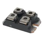
SOT-227 Power Module
High Side Chopper - Power MOSFET, 100 A
FEATURES
3
(D)
MOSFET
• Enhanced body diode dV/dt and dIF/dt capability
• Improved gate avalanche and dynamic dV/dt
ruggedness
2
(G)
1
(S, K)
• Fully characterized capacitance and avalanche SOA
• Fully isolated package
• Easy to use and parallel
4
(A)
SOT-227
• Low on-resistance
PRIMARY CHARACTERISTICS
• Simple drive requirements
MOSFET
VDSS
200 V
RDS(on)
9.6 m
ID at 97 °C
80 A
Type
Modules - MOSFET
Package
CHOPPER DIODE
• Low forward voltage drop
• Ultrafast, soft reverse recovery, with high operating
junction temperature (TJ max. = 175 °C)
• UL approved file E78996
SOT-227
IF at 90 °C
64 A
• Material categorization: for definitions of compliance
please see www.vishay.com/doc?99912
trr
33 ns
CHOPPER DIODE
ABSOLUTE MAXIMUM RATINGS
PARAMETER
SYMBOL
TEST CONDITIONS
MAX.
UNITS
200
V
MOSFET
Drain to source voltage
Continuous drain current VGS at 10 V
Pulsed drain current
Power dissipation
Gate to source voltage
Single pulse avalanche energy
VDSS
ID
TC = 25 °C
TC = 90 °C
IDM (1)
PD
108
83
A
170
TC = 25 °C
405
TC = 90 °C
229
W
VGS
± 30
V
EAS (2)
600
mJ
Avalanche current
IAR (3)
50
A
Repetitive avalanche energy
EAR (3)
300
mJ
200
V
CHOPPER DIODE
Cathode to anode voltage
Continuous forward current
Maximum peak one cycle non-repetitive surge current
Maximum power dissipation, chopper diode
VR
IF
TC = 25 °C
92
TC = 90 °C
64
IFSM
PD
Tc = 90 °C
A
280
A
79
W
MODULE
Operating junction temperature range
TJ
-55 to +175
Storage temperature range
TStg
-55 to +175
RMS insulation voltage
VISO
Any terminal to case, t = 1 min
2500
°C
V
Notes
(1) Repetitive rating; pulse width limited by maximum junction temperature starting T = 25 °C
J
(2) Limited by T max., starting T = 25 °C, L = 0.23 mH, R = 25 , I
J
J
g
AS = 72 A, VGS = 10 V. Part not recommended for use above this value
(3) Repetitive rating; pulse width limited by maximum junction temperature starting T = 25 °C, L = 0.23 mH, R = 25 , V
J
g
GS = 10 V, duty cycle 1 %
Revision: 10-Sep-2019
Document Number: 94856
1
For technical questions within your region: DiodesAmericas@vishay.com, DiodesAsia@vishay.com, DiodesEurope@vishay.com
THIS DOCUMENT IS SUBJECT TO CHANGE WITHOUT NOTICE. THE PRODUCTS DESCRIBED HEREIN AND THIS DOCUMENT
ARE SUBJECT TO SPECIFIC DISCLAIMERS, SET FORTH AT www.vishay.com/doc?91000
�VS-FC80NA20
www.vishay.com
Vishay Semiconductors
THERMAL - MECHANICAL SPECIFICATIONS
PARAMETER
Junction to case thermal resistance
Case to sink, flat greased surface (heatsink
compound thermal conductivity = 1 W/mK)
SYMBOL
MOSFET
Chopper Diode
Module
MIN.
TYP.
MAX.
-
-
0.37
-
-
1.08
-
0.10
-
RthJC
RthCS
Mounting torque
UNITS
°C/W
Torque to terminal
-
-
1.1 (9.7)
Torque to heatsink
-
-
1.8 (15.9) Nm (lbf.in)
-
30
Approximate module weight
Nm (lbf.in)
-
g
ELECTRICAL CHARACTERISTICS (TJ = 25 °C unless otherwise specified)
PARAMETER
SYMBOL
TEST CONDITIONS
MIN.
TYP.
MAX.
UNITS
MOSFET
Drain-to-source breakdown voltage
Breakdown voltage temperature coefficient
Static drain-to-source on-resistance
Gate threshold voltage
Forward transconductance
Drain-to-source leakage current
Gate-to-source forward leakage
Gate-to-source reverse leakage
Total gate charge
V(BR)DSS
V(BR)DSS/TJ
RDS(on) (1)
VGS(th)
gfs
IDSS
IGSS
Qg
Gate-to-source charge
Qgs
Gate-to-drain (“Miller”) charge
Qgd
Turn-on delay time
td(on)
Rise time
Turn-off delay time
Fall time
Turn-on delay time
Rise time
Turn-off delay time
VGS = 10 V, ID = 80 A
-
-
V
-
0.21
-
V/°C
m
-
9.6
14.0
2.7
4.1
5.5
VDS = VGS, ID = 250 μA , TJ = 125 °C
-
2.6
-
VDS = 20 V, ID = 80 A
-
200
-
VDS = 200 V, VGS = 0 V
-
0.6
25
VDS = 200 V, VGS = 0 V, TJ = 125 °C
-
20
500
VDS = 200 V, VGS = 0 V, TJ = 175 °C
-
1
5
VGS = 20 V
-
-
120
VGS = -20 V
-
-
-120
-
161
-
-
54
-
-
52
-
VDS = VGS, ID = 250 μA
ID = 80 A, VDS = 100 V, VGS = 10 V,
see fig. 15 and fig. 28 (1)
-
148
-
215
-
-
114
-
tf
-
125
-
td(on)
-
132
-
-
215
-
-
124
-
-
108
-
-
3
-
-
10 720
-
td(off)
tr
td(off)
Fall time
tf
LS
Ciss
Coss
VDD = 100 V, ID = 80 A, Rg = 2.5 ,
L = 500 μH
VDD = 100 V, ID = 80 A, Rg = 2.5 ,
L = 500 μH, TJ = 125 °C
Between lead and center of die contact
VGS = 0 V, VDS = 50 V, f = 1.0 MHz,
see fig. 14
Crss
Drain to Case Capacitance
200
-
tr
Internal source inductance
Input capacitance
VGS = 0 V, ID = 500 μA
Reference to 25 °C, ID = 1 mA
Cd-cs
VGS = 0 V, (G-S shorted); f = 1 MHz
VBR
IR = 100 μA
-
810
-
-
160
-
-
50
-
V
S
μA
mA
nA
nC
ns
ns
nH
pF
CHOPPER DIODE
Diode reverse breakdown voltage
Forward voltage drop
VFM
200
-
-
IF = 30 A
-
0.94
1.08
IF = 30 A, TJ = 125 °C
-
0.8
-
IF = 30 A, TJ = 175 °C
-
0.74
-
VR = VR rated
-
1
50
-
7
-
V
μA
Reverse leakage current
IRM
VR = VR rated, TJ = 125 °C
VR = VR rated, TJ = 175 °C
-
0.15
1
mA
Junction capacitance
CT
VR = 200 V
-
119
-
pF
Note
(1) Pulse width 400 μs, duty cycle 2 %
Revision: 10-Sep-2019
Document Number: 94856
2
For technical questions within your region: DiodesAmericas@vishay.com, DiodesAsia@vishay.com, DiodesEurope@vishay.com
THIS DOCUMENT IS SUBJECT TO CHANGE WITHOUT NOTICE. THE PRODUCTS DESCRIBED HEREIN AND THIS DOCUMENT
ARE SUBJECT TO SPECIFIC DISCLAIMERS, SET FORTH AT www.vishay.com/doc?91000
�VS-FC80NA20
www.vishay.com
Vishay Semiconductors
SOURCE-DRAIN RATINGS AND CHARACTERISTICS (TJ = 25 °C unless otherwise specified)
PARAMETER
SYMBOL
TEST CONDITIONS
MIN.
TYP.
MAX.
IS
UNITS
MOSFET
-
108
ISM (1)
MOSFET symbol showing the integral
reverse p-n junction diode
-
Pulsed source current (body diode)
-
-
170
TJ = 25 °C, IS = 80 A, VGS = 0 V
-
0.88
1.02
Body diode forward voltage
VSD (2)
TJ = 125 °C, IS = 80 A, VGS = 0 V
-
0.76
-
TJ = 175 °C, IS = 80 A, VGS = 0 V
-
0.70
-
-
145
-
-
11
-
A
-
790
-
nC
ns
Continuous source current (body diode)
Reverse recovery time
trr
Reverse recovery current
Irr
Reverse recovery charge
Qrr
Reverse recovery time
trr
Reverse recovery current
Irr
Reverse recovery charge
Qrr
Forward turn-on time
ton
TJ = 25 °C, IF = 30 A, dIF/dt = 100 A/μs,
VR = 100 V (2)
TJ = 125 °C, IF = 30 A, dIF/dt = 100 A/μs,
VR = 100 V (2)
A
V
ns
-
170
-
-
13.5
-
A
-
1140
-
nC
Intrinsic turn-on time is negligible (turn-on is dominated by LS + LD)
DYNAMIC RECOVERY CHARACTERISTICS (TJ = 25 °C unless otherwise specified)
PARAMETER
SYMBOL
TEST CONDITIONS
MIN.
TYP.
MAX.
UNITS
ns
CHOPPER DIODE
Reverse recovery time
trr
Reverse recovery current
Irr
Reverse recovery charge
Qrr
Reverse recovery time
trr
Reverse recovery current
Irr
Reverse recovery charge
Qrr
TJ = 25 °C, IF = 30 A, dIF/dt = 200 A/μs,
VR = 100 V (2)
TJ = 25 °C, IF = 30 A, dIF/dt = 200 A/μs,
VR = 100 V (2)
-
33
-
-
3.5
-
A
-
59
-
nC
ns
-
59
-
-
8.3
-
A
-
238
-
nC
Notes
(1) Repetitive rating, pulse width limited by maximum junction temperature (see fig. 27)
(2) Pulse width 300 μs, duty cycle 2 %
1000
175
150
100
125
DC
ID (A)
Allowable Case Temperature (°C)
200
100
75
TJ = 25 °C
TJ = 125 °C
TJ = 175 °C
10
50
25
0
0
25
50
75
100
125
1
0.01
0.1
1
10
ID - Continuous Drain Current (A)
VDS (V)
Fig. 1 - Maximum MOSFET Drain-Source Current vs.
Case Temperature
Fig. 2 - Typical MOSFET Output Characteristics,
VGS = 10 V
Revision: 10-Sep-2019
Document Number: 94856
3
For technical questions within your region: DiodesAmericas@vishay.com, DiodesAsia@vishay.com, DiodesEurope@vishay.com
THIS DOCUMENT IS SUBJECT TO CHANGE WITHOUT NOTICE. THE PRODUCTS DESCRIBED HEREIN AND THIS DOCUMENT
ARE SUBJECT TO SPECIFIC DISCLAIMERS, SET FORTH AT www.vishay.com/doc?91000
�VS-FC80NA20
www.vishay.com
Vishay Semiconductors
35
200
180
160
140
ID (A)
120
RDS(on) - Drain-to-Source
On-Resistance (mΩ)
VGE = 7 V
VGE = 8 V
VGE = 9 V
VGE = 10 V
VGE = 12 V
VGE = 15 V
100
80
60
40
ID = 80 A
VGS = 10 V
30
25
20
15
10
20
5
0
0
0.5
1
1.5
2
2.5
0
3
50
75
125
150
175
200
TJ (°C)
Fig. 3 - Typical MOSFET Output Characteristics,
at TJ = 25 °C
Fig. 6 - Typical Drain to Source On-Resistance vs. Temperature
100
VGE = 7 V
VGE = 8 V
VGE = 9 V
VGE = 10 V
VGE = 12 V
VGE = 15 V
180
160
140
VDS = 20 V
90
80
70
60
ID (A)
120
100
TJ = 125 °C
50
80
40
60
30
40
20
20
10
TJ = 25 °C
0
0
0
1
2
3
4
5
3
6
4
5
6
7
8
VGS (V)
VDS (V)
Fig. 4 - Typical MOSFET Output Characteristics,
at TJ = 125 °C
Fig. 7 - Typical MOSFET Transfer Characteristics
5.0
200
VGE = 7 V
VGE = 8 V
VGE = 9 V
VGE = 10 V
VGE = 12 V
VGE = 15 V
160
140
120
4.5
TJ = 25 °C
4.0
VGEth (V)
180
ID (A)
100
VDS (V)
200
ID (A)
25
100
80
3.5
TJ = 125 °C
3.0
60
40
2.5
20
2.0
0
0
1
2
3
4
5
6
7
8
0.2
0.3
0.4
0.5
0.6
0.7
0.8
0.9
1.0
VDS (V)
ID (mA)
Fig. 5 - Typical MOSFET Output Characteristics,
at TJ = 175 °C
Fig. 8 - Typical MOSFET Gate Threshold Voltage
Revision: 10-Sep-2019
Document Number: 94856
4
For technical questions within your region: DiodesAmericas@vishay.com, DiodesAsia@vishay.com, DiodesEurope@vishay.com
THIS DOCUMENT IS SUBJECT TO CHANGE WITHOUT NOTICE. THE PRODUCTS DESCRIBED HEREIN AND THIS DOCUMENT
ARE SUBJECT TO SPECIFIC DISCLAIMERS, SET FORTH AT www.vishay.com/doc?91000
�VS-FC80NA20
www.vishay.com
Vishay Semiconductors
100
200
90
180
80
160
70
140
120
IF (A)
ISD (A)
60
TJ = 25 °C
TJ = 125 °C
TJ = 150 °C
50
40
100
TJ = 175 °C
80
30
60
20
40
10
20
0
TJ = 125 °C
TJ = 25 °C
0
0
0.2
0.4
0.6
0.8
1.0
1.2
0.2
0.4
0.6
0.8
1.0
1.2
1.4
1.6
1.8
VSD (V)
VFM (V)
Fig. 9 - Typical MOSFET Body Diode Forward Current Characteristics
Fig. 12 - Typical Chopper Diode Forward Characteristics
10
1
0.1
0.1
IRM (mA)
IDSS (mA)
Tj = 175 °C
TJ = 175 °C
1
TJ = 125 °C
0.01
0.001
0.01
Tj = 125 °C
0.001
Tj = 25 °C
TJ = 25 °C
0.0001
0.0001
50
75
100
125
150
175
200
50
75
100
VDSS (V)
150
175
200
VR (V)
Fig. 13 - Typical Chopper Diode Reverse Leakage Current
Fig. 10 - Typical MOSFET Zero Gate Voltage Drain Current
1000
200
175
150
125
Switching Time (ns)
Allowable Case Temperature (°C)
125
DC
100
75
50
tr
td(on)
100
td(off)
tf
25
0
10
0
20
40
60
80
100
0
10
20
30
40
50
60
70
80
90
IF(AV) - Average Forward Current (A)
ID (A)
Fig. 11 - Maximum Allowable Forward Current vs. Case Temperature
Fig. 14 - Typical MOSFET Switching Time vs. ID
TJ = 125 °C, VDD = 100 V, Rg = 2.5 , VGS = 10 V, L = 500 μH
Revision: 10-Sep-2019
Document Number: 94856
5
For technical questions within your region: DiodesAmericas@vishay.com, DiodesAsia@vishay.com, DiodesEurope@vishay.com
THIS DOCUMENT IS SUBJECT TO CHANGE WITHOUT NOTICE. THE PRODUCTS DESCRIBED HEREIN AND THIS DOCUMENT
ARE SUBJECT TO SPECIFIC DISCLAIMERS, SET FORTH AT www.vishay.com/doc?91000
�VS-FC80NA20
www.vishay.com
Vishay Semiconductors
1000
18
14
td(on)
td(off)
TJ = 125 °C
12
100
Irr (A)
Switching Time (ns)
16
tr
tf
10
8
TJ = 25 °C
6
4
2
10
0
2
4
6
8
10
12
14
16
100
200
Rg (Ω)
400
500
dIF/dt (A/μs)
Fig. 15 - Typical MOSFET Switching Time vs. Rg
TJ = 125 °C, VDD = 100 V, ID = 80 A, L = 500 μH
Fig. 17 - Typical Chopper Diode Reverse Recovery Current vs. dIF/dt
Vrr = 100 V, IF = 30 A
80
500
75
450
70
400
65
TJ = 125 °C
350
60
TJ = 125 °C
55
Qrr (nC)
trr (ns)
300
50
45
40
300
250
200
150
35
TJ = 25 °C
TJ = 25 °C
100
30
50
25
0
20
100
200
300
400
100
500
200
300
400
500
dIF/dt (A/μs)
dIF/dt (A/μs)
Fig. 16 - Typical Chopper Diode Reverse Recovery Time vs. dIF/dt
Vrr = 100 V, IF = 30 A
Fig. 18 - Typical Chopper Diode Reverse Recovery Charge vs. dIF/dt
Vrr = 100 V, IF = 30 A
ZthJC - Thermal Impedance
Junction to Case (°C/W)
1
0.1
0.75
0.50
0.25
0.10
0.05
0.02
DC
0.01
0.001
0.00001
0.0001
0.001
0.01
0.1
1
10
t1 - Rectangular Pulse Duration (s)
Fig. 19 - Maximum Thermal Impedance ZthJC Characteristics - (MOSFET)
Revision: 10-Sep-2019
Document Number: 94856
6
For technical questions within your region: DiodesAmericas@vishay.com, DiodesAsia@vishay.com, DiodesEurope@vishay.com
THIS DOCUMENT IS SUBJECT TO CHANGE WITHOUT NOTICE. THE PRODUCTS DESCRIBED HEREIN AND THIS DOCUMENT
ARE SUBJECT TO SPECIFIC DISCLAIMERS, SET FORTH AT www.vishay.com/doc?91000
�VS-FC80NA20
www.vishay.com
Vishay Semiconductors
ZthJC - Thermal Impedance
Junction to Case (°C/W)
10
1
0.1
0.75
0.50
0.25
0.10
0.05
0.02
DC
0.01
0.001
0.00001
0.0001
0.001
0.01
0.1
1
10
t1 - Rectangular Pulse Duration (s)
Fig. 20 - Maximum Thermal Impedance Characteristics (Chopper Diode)
CIRCUIT CONFIGURATION
CIRCUIT
CIRCUIT CONFIGURATION CODE
CIRCUIT DRAWING
3
(D)
3
(D)
2
(G)
4
(A)
1
(S, K)
2
(G)
1
(S, K)
High side chopper
4
(A)
N
4
3
1
2
Revision: 10-Sep-2019
Document Number: 94856
7
For technical questions within your region: DiodesAmericas@vishay.com, DiodesAsia@vishay.com, DiodesEurope@vishay.com
THIS DOCUMENT IS SUBJECT TO CHANGE WITHOUT NOTICE. THE PRODUCTS DESCRIBED HEREIN AND THIS DOCUMENT
ARE SUBJECT TO SPECIFIC DISCLAIMERS, SET FORTH AT www.vishay.com/doc?91000
�VS-FC80NA20
www.vishay.com
Vishay Semiconductors
ORDERING INFORMATION TABLE
Device code
VS-
F
C
80
N
A
20
1
2
3
4
5
6
7
1
-
Vishay Semiconductors product
2
-
MOSFET module
3
-
MOSFET die generation
4
-
Current rating (80 = 80 A)
5
-
N = high side chopper
6
-
Package indicator SOT-227
7
-
Voltage rating (20 = 200 V)
LINKS TO RELATED DOCUMENTS
Dimensions
www.vishay.com/doc?95423
Packaging information
www.vishay.com/doc?95425
Revision: 10-Sep-2019
Document Number: 94856
8
For technical questions within your region: DiodesAmericas@vishay.com, DiodesAsia@vishay.com, DiodesEurope@vishay.com
THIS DOCUMENT IS SUBJECT TO CHANGE WITHOUT NOTICE. THE PRODUCTS DESCRIBED HEREIN AND THIS DOCUMENT
ARE SUBJECT TO SPECIFIC DISCLAIMERS, SET FORTH AT www.vishay.com/doc?91000
�Outline Dimensions
www.vishay.com
Vishay Semiconductors
SOT-227 Generation 2
DIMENSIONS in millimeters (inches)
37.80 (1.488)
38.30 (1.508)
Ø 4.10 (0.161)
Ø 4.30 (0.169)
-A-
4 x M4 nuts
6.25 (0.246)
6.50 (0.256)
12.50 (0.492)
13.00 (0.512)
7.45 (0.293)
7.60 (0.299)
14.90 (0.587)
15.20 (0.598)
24.70 (0.972)
25.70 (1.012)
R full 2.07 (0.081)
2.12 (0.083)
29.80 (1.173)
30.50 (1.200)
31.50 (1.240)
32.10 (1.264)
4x
1.90 (0.075)
2.20 (0.087)
7.70 (0.303)
8.30 (0.327)
0.25 (0.010) M C A M B M
4.10 (0.161)
4.50 (0.177)
5.33 (0.210)
5.96 (0.234)
11.60 (0.457)
12.30 (0.484)
24.70 (0.972)
25.50 (1.004)
Note
• Controlling dimension: millimeter
Document Number: 95423
1
For technical questions, contact: DiodesAmericas@vishay.com
THIS DOCUMENT IS SUBJECT TO CHANGE WITHOUT NOTICE. THE PRODUCTS DESCRIBED HEREIN AND THIS DOCUMENT
ARE SUBJECT TO SPECIFIC DISCLAIMERS, SET FORTH AT www.vishay.com/doc?91000
Revision: 19-May-2020
�Legal Disclaimer Notice
www.vishay.com
Vishay
Disclaimer
ALL PRODUCT, PRODUCT SPECIFICATIONS AND DATA ARE SUBJECT TO CHANGE WITHOUT NOTICE TO IMPROVE
RELIABILITY, FUNCTION OR DESIGN OR OTHERWISE.
Vishay Intertechnology, Inc., its affiliates, agents, and employees, and all persons acting on its or their behalf (collectively,
“Vishay”), disclaim any and all liability for any errors, inaccuracies or incompleteness contained in any datasheet or in any other
disclosure relating to any product.
Vishay makes no warranty, representation or guarantee regarding the suitability of the products for any particular purpose or
the continuing production of any product. To the maximum extent permitted by applicable law, Vishay disclaims (i) any and all
liability arising out of the application or use of any product, (ii) any and all liability, including without limitation special,
consequential or incidental damages, and (iii) any and all implied warranties, including warranties of fitness for particular
purpose, non-infringement and merchantability.
Statements regarding the suitability of products for certain types of applications are based on Vishay's knowledge of typical
requirements that are often placed on Vishay products in generic applications. Such statements are not binding statements
about the suitability of products for a particular application. It is the customer's responsibility to validate that a particular product
with the properties described in the product specification is suitable for use in a particular application. Parameters provided in
datasheets and / or specifications may vary in different applications and performance may vary over time. All operating
parameters, including typical parameters, must be validated for each customer application by the customer's technical experts.
Product specifications do not expand or otherwise modify Vishay's terms and conditions of purchase, including but not limited
to the warranty expressed therein.
Hyperlinks included in this datasheet may direct users to third-party websites. These links are provided as a convenience and
for informational purposes only. Inclusion of these hyperlinks does not constitute an endorsement or an approval by Vishay of
any of the products, services or opinions of the corporation, organization or individual associated with the third-party website.
Vishay disclaims any and all liability and bears no responsibility for the accuracy, legality or content of the third-party website
or for that of subsequent links.
Except as expressly indicated in writing, Vishay products are not designed for use in medical, life-saving, or life-sustaining
applications or for any other application in which the failure of the Vishay product could result in personal injury or death.
Customers using or selling Vishay products not expressly indicated for use in such applications do so at their own risk. Please
contact authorized Vishay personnel to obtain written terms and conditions regarding products designed for such applications.
No license, express or implied, by estoppel or otherwise, to any intellectual property rights is granted by this document or by
any conduct of Vishay. Product names and markings noted herein may be trademarks of their respective owners.
© 2022 VISHAY INTERTECHNOLOGY, INC. ALL RIGHTS RESERVED
Revision: 01-Jan-2022
1
Document Number: 91000
�