VS-SD1053C..L Series
www.vishay.com
Vishay Semiconductors
Fast Recovery Diodes
(Hockey PUK Version), 920 A, 1050 A
FEATURES
• High power fast recovery diode series
• 2.0 μs to 3.0 μs recovery time
• High voltage ratings up to 3000 V
• High current capability
• Optimized turn-on and turn-off characteristics
• Low forward recovery
• Fast and soft reverse recovery
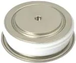
• Press PUK encapsulation
• Case style conform to JEDEC® B-PUK (DO-200AB)
B-PUK (DO-200AB)
• Maximum junction temperature 150 °C
• Designed and qualified for industrial level
PRIMARY CHARACTERISTICS
IF(AV)
920 A, 1050 A
Package
B-PUK (DO-200AB)
Circuit configuration
Single
• Material categorization: for definitions of compliance
please see www.vishay.com/doc?99912
TYPICAL APPLICATIONS
• Snubber diode for GTO
• High voltage freewheeling diode
• Fast recovery rectifier applications
MAJOR RATINGS AND CHARACTERISTICS
PARAMETER
SD1053C..L
TEST CONDITIONS
IF(AV)
Ths
IF(RMS)
IFSM
VRRM
trr
UNITS
S20
S30
1050
920
A
55
55
°C
1940
1700
50 Hz
15 000
13 000
60 Hz
15 700
13 610
Range
1800 to 2500
1800 to 3000
V
2.0
3.0
μs
TJ
25
°C
-40 to +150
TJ
A
ELECTRICAL SPECIFICATIONS
VOLTAGE RATINGS
TYPE NUMBER
VS-SD1053C..S20L
VS-SD1053C..S30L
VOLTAGE
CODE
VRRM, MAXIMUM REPETITIVE
PEAK REVERSE VOLTAGE
V
VRSM, MAXIMUM NON-REPETITIVE
PEAK REVERSE VOLTAGE
V
18
1800
1900
22
2200
2300
24
2400
2500
25
2500
2600
18
1800
1900
22
2200
2300
25
2500
2600
28
2800
2900
30
3000
3100
IRRM MAXIMUM
AT TJ = TJ MAXIMUM
mA
50
Revision: 11-Jan-18
Document Number: 93167
1
For technical questions within your region: DiodesAmericas@vishay.com, DiodesAsia@vishay.com, DiodesEurope@vishay.com
THIS DOCUMENT IS SUBJECT TO CHANGE WITHOUT NOTICE. THE PRODUCTS DESCRIBED HEREIN AND THIS DOCUMENT
ARE SUBJECT TO SPECIFIC DISCLAIMERS, SET FORTH AT www.vishay.com/doc?91000
�VS-SD1053C..L Series
www.vishay.com
Vishay Semiconductors
FORWARD CONDUCTION
PARAMETER
SYMBOL
Maximum average forward current
at heatsink temperature
IF(AV)
IF(RMS)
Maximum RMS forward current
Maximum peak, one-cycle forward,
non-repetitive surge current
IFSM
SD1053C..L
UNITS
S20
S30
1050 (450) 920 (390)
A
55 (85)
55 (85)
°C
1940
1700
15 000
13 000
15 700
13 610
A
12 620
10 930
13 210
11 450
1125
845
1027
772
kA2s
796
598
727
546
11 250
8450
kA2s
1.34
1.51
V
1.48
1.67
TEST CONDITIONS
180° conduction, half sine wave
Double side (single side) cooled
25 °C heatsink temperature double side cooled
t = 10 ms
No voltage
reapplied
t = 8.3 ms
VF(TO)1
VF(TO)2
t = 10 ms
100 % VRRM
reapplied
t = 8.3 ms
Sinusoidal half wave,
initial TJ = TJ maximum
t = 10 ms
No voltage
reapplied
t = 8.3 ms
t = 10 ms
100 % VRRM
reapplied
t = 8.3 ms
t = 0.1 to 10 ms, no voltage reapplied
(16.7 % x x IF(AV) < I < x IF(AV)), TJ = TJ maximum
(I > x IF(AV)), TJ = TJ maximum
rf1
(16.7 % x x IF(AV) < I < x IF(AV)), TJ = TJ maximum
0.37
0.50
rf2
(I > x IF(AV)), TJ = TJ maximum
0.33
0.45
Ipk = 1500 A, TJ = TJ maximum,
tp = 10 ms sinusoidal wave
1.90
2.26
Maximum I2t for fusing
I2t
Maximum I2t for fusing
Low level value of threshold voltage
High level value of threshold voltage
Low level value of forward
slope resistance
High level value of forward
slope resistance
I2t
m
VFM
Maximum forward voltage drop
V
RECOVERY CHARACTERISTICS
MAXIMUM VALUE
AT TJ = 25 °C
CODE
Ipk
SQUARE
PULSE
(A)
trr AT 25 % IRRM
(μs)
S20
2.0
S30
3.0
TYPICAL VALUES
AT TJ = 150 °C
TEST CONDITIONS
1000
IFM
dI/dt
(A/μs)
Vr
(V)
100
trr AT 25 % IRRM
(μs)
- 50
Qrr
(μC)
Irr
(A)
4.0
400
180
4.5
550
230
trr
t
dir
dt
Qrr
IRM(REC)
THERMAL AND MECHANICAL SPECIFICATIONS
PARAMETER
Maximum junction operating
and storage temperature range
SYMBOL
TEST CONDITIONS
TJ, TStg
Maximum thermal resistance,
case junction to heatsink
RthJ-hs
Mounting force, ± 10 %
Approximate weight
Case style
DC operation single side cooled
DC operation double side cooled
See dimensions - link at the end of datasheet
VALUES
UNITS
-40 to 150
°C
0.073
K/W
0.031
14 700 (1500)
N (kg)
255
g
B-PUK (DO-200AB)
RthJ-hs CONDUCTION
CONDUCTION ANGLE
180°
120°
90°
60°
30°
SINUSOIDAL CONDUCTION
RECTANGULAR CONDUCTION
SINGLE SIDE
DOUBLE SIDE
SINGLE SIDE
DOUBLE SIDE
0.009
0.011
0.014
0.020
0.036
0.008
0.011
0.014
0.021
0.036
0.006
0.011
0.015
0.021
0.036
0.006
0.011
0.015
0.022
0.036
TEST CONDITIONS
UNITS
TJ = TJ maximum
K/W
Note
• The table above shows the increment of thermal resistance RthJ-hs when devices operate at different conduction angles than DC
Revision: 11-Jan-18
Document Number: 93167
2
For technical questions within your region: DiodesAmericas@vishay.com, DiodesAsia@vishay.com, DiodesEurope@vishay.com
THIS DOCUMENT IS SUBJECT TO CHANGE WITHOUT NOTICE. THE PRODUCTS DESCRIBED HEREIN AND THIS DOCUMENT
ARE SUBJECT TO SPECIFIC DISCLAIMERS, SET FORTH AT www.vishay.com/doc?91000
�VS-SD1053C..L Series
160
Vishay Semiconductors
SD1053C..S20L Series
(Single Side Cooled)
RthJ-hs (DC) = 0.073 K/ W
140
120
Conduction Angle
100
80
60
30°
180°
60°
90°
120°
40
0
100
200
300
400
500
600
700
Maximum Allowable Heatsink Temperature (°C)
Maximum Allowable Heatsink Temperature (°C)
www.vishay.com
160
SD1053C..S30L Series
(Single Side Cooled)
R thJ-hs (DC) = 0.073 K/ W
140
120
100
Conduc tion Period
80
60
30°
60°
40
90°
120°
20
0
160
SD1053C..S20L Series
(Single Side Cooled)
RthJ-hs (DC) = 0.073 K/ W
120
100
Conduction Period
80
30°
60°
90°
40
120°
180° DC
20
0
200
400
600
800
1000 1200
Conduction Angle
80
30°
40
60°
90°
120°
180°
20
0
100
200
300
400
500
Average Forward Current (A)
Fig. 3 - Current Ratings Characteristics
600
Maximum Allowable Heatsink Temperature (°C)
Maximum Allowable Heatsink Temp erature (°C)
120
60
800
1000
SD1053C..S20L Series
(Double Side Cooled)
R thJ-hs (DC) = 0.031 K/ W
140
120
100
Conduction Angle
80
60
30°
60°
90°
40
120° 180°
20
0
0
200
400
600
800 1000 1200 1400
Fig. 5 - Current Ratings Characteristics
SD1053C..S30L Series
(Single Side Cooled)
RthJ-hs (DC) = 0.073 K/ W
100
600
Average Forward Current (A)
Fig. 2 - Current Ratings Characteristics
140
400
160
Average Forward Current (A)
160
200
Fig. 4 - Current Ratings Characteristics
Maximum Allowable Heatsink Temperature (°C)
Maximum Allowable Heatsink Temperature (°C)
Fig. 1 - Current Ratings Characteristics
60
DC
Average Forward Current (A)
Average Forward Current (A)
140
180°
0
160
SD1053C..S20L Series
(Double Side Cooled)
RthJ-hs (DC) = 0.031 K/ W
140
120
100
Conduction Period
80
30°
60
60°
90°
40
120°
180°
20
DC
0
0
400
800
1200
1600
2000
Average Forward Current (A)
Fig. 6 - Current Ratings Characteristics
Revision: 11-Jan-18
Document Number: 93167
3
For technical questions within your region: DiodesAmericas@vishay.com, DiodesAsia@vishay.com, DiodesEurope@vishay.com
THIS DOCUMENT IS SUBJECT TO CHANGE WITHOUT NOTICE. THE PRODUCTS DESCRIBED HEREIN AND THIS DOCUMENT
ARE SUBJECT TO SPECIFIC DISCLAIMERS, SET FORTH AT www.vishay.com/doc?91000
�VS-SD1053C..L Series
160
Vishay Semiconductors
SD1053C..S30L Series
(Double Side Cooled)
RthJ-hs (DC) = 0.031 K/ W
140
120
100
Conduction Angle
80
60
40
20
90° 120°
60°
30°
180°
0
0
200
400
600
800
Maximum Average Forward Power Loss (W)
Maximum Allowable Heatsink Temperature (°C)
www.vishay.com
4500
DC
180°
120°
90°
60°
30°
4000
3500
3000
2500
RMSLimit
2000
1500
Conduction Period
1000
SD1053C..S20L Series
TJ = 150°C
500
0
0
1000 1200
Average Forward Current (A)
160
SD1053C..S30L Series
(Double Side Cooled)
RthJ-hs (DC) = 0.031 K/ W
120
100
Conduction Period
80
30°
60
60°
90°
120°
40
180°
20
DC
0
0
400
800
1200
1600
2000
3500
2500
2000
RMSLimit
1500
1000
Conduction Angle
500
SD1053C..S20L Series
TJ = 150°C
0
0
200
400
1600
2000
2800
180°
120°
90°
60°
30°
2400
2000
600 800 1000 1200 1400
Average Forward Current (A)
Fig. 9 - Forward Power Loss Characteristics
RMS Limit
1600
1200
Conduction Angle
800
SD1053C..S30L Series
TJ = 150°C
400
0
0
200
400
600
800
1000 1200
Average Forward Current (A)
Fig. 11 - Forward Power Loss Characteristics
Maximum Average Forward Power Loss (W)
Maximum Average Forward Power Loss (W)
Fig. 8 - Current Ratings Characteristics
180°
120°
90°
60°
30°
1200
3200
Average Forward Current (A)
3000
800
Fig. 10 - Forward Power Loss Characteristics
Maximum Average Forward Power Loss (W)
Maximum Allowable Heatsink Temperature (°C)
Fig. 7 - Current Ratings Characteristics
140
400
Average Forward Current (A)
4500
DC
180°
120°
90°
60°
30°
4000
3500
3000
2500
RMS Limit
2000
Conduction Period
1500
1000
SD1053C..S30L Series
TJ = 150°C
500
0
0
400
800
1200
1600
2000
Average Forward Current (A)
Fig. 12 - Forward Power Loss Characteristics
Revision: 11-Jan-18
Document Number: 93167
4
For technical questions within your region: DiodesAmericas@vishay.com, DiodesAsia@vishay.com, DiodesEurope@vishay.com
THIS DOCUMENT IS SUBJECT TO CHANGE WITHOUT NOTICE. THE PRODUCTS DESCRIBED HEREIN AND THIS DOCUMENT
ARE SUBJECT TO SPECIFIC DISCLAIMERS, SET FORTH AT www.vishay.com/doc?91000
�VS-SD1053C..L Series
14000
Vishay Semiconductors
Peak Half Sine Wave Forward Current (A)
Peak Half Sine Wave Forward Current (A)
www.vishay.com
At Any Rated Load Condition And With
Rated VRRM Applied Following Surge.
Initial TJ = 150 °C
@60 Hz 0.0083 s
@50 Hz 0.0100 s
13000
12000
11000
10000
9000
8000
7000
6000
SD1053C..S20L Series
5000
4000
1
10
100
13000
12000
11000
10000
Maximum Non Repetitive Surg e Current
Versus Pulse Train Duration.
Initial TJ = 150 °C
No Voltag e Reapplied
Rated VRRM Reapplied
9000
8000
7000
6000
5000
SD1053C..S30L Series
4000
3000
0.01
0.1
Fig. 16 - Maximum Non-Repetitive Surge Current
Single and Double Side Cooled
10000
16000
Maximum Non Repetitive Surge Current
Versus Pulse Train Duration.
14000
Initial TJ = 150 °C
No Voltage Reapplied
12000
Rated VRRM Reapplied
10000
8000
6000
SD1053C..S20L Series
4000
2000
0.01
Instantaneous Forward Current (A)
Peak Half Sine Wave Forward Current (A)
Fig. 13 - Maximum Non-Repetitive Surge Current
TJ = 25°C
TJ = 150°C
1000
SD1053C..S20L Series
100
0.1
1
1
Pulse Train Duration (s)
1.5
2
2.5
3
3.5
4
4.5
5
Instantaneous Forward Voltage (V)
Fig. 14 - Maximum Non-Repetitive Surge Current
Fig. 17 - Forward Voltage Drop Characteristics
10000
12000
At Any Rated Load Condition And With
Rated VRRM Applied Following Surge.
Initial TJ = 150°C
@60 Hz 0.0083 s
@50 Hz 0.0100 s
11000
10000
9000
8000
7000
6000
5000
SD1053C..S30L Series
4000
3000
Instantaneous Forward Current (A)
Peak Half Sine Wave Forward Current (A)
1
Pulse Train Dura tion (s)
Number Of Equa l Amplitude Half Cycle Current Pulses (N)
TJ = 25°C
TJ = 150°C
1000
SD1053C..S30L Series
100
1
10
100
Number Of Equa l Amplitude Half Cyc le Current Pulses (N)
Fig. 15 - Maximum Non-Repetitive Surge Current
Single and Double Side Cooled
1 1.5 2 2.5 3 3.5 4 4.5 5 5.5 6 6.5
Instantaneous Forward Voltage (V)
Fig. 18 - Forward Voltage Drop Characteristics
Revision: 11-Jan-18
Document Number: 93167
5
For technical questions within your region: DiodesAmericas@vishay.com, DiodesAsia@vishay.com, DiodesEurope@vishay.com
THIS DOCUMENT IS SUBJECT TO CHANGE WITHOUT NOTICE. THE PRODUCTS DESCRIBED HEREIN AND THIS DOCUMENT
ARE SUBJECT TO SPECIFIC DISCLAIMERS, SET FORTH AT www.vishay.com/doc?91000
�VS-SD1053C..L Series
Transient Thermal Impedance Z thJ-hs (K/ W)
www.vishay.com
Vishay Semiconductors
0.1
SD1053C..S20/ S30L Series
Steady State Value
0.01
R thJ-hs = 0.073 K/ W
(Single Side Cooled)
R thJ-hs = 0.031 K/ W
(Double Side Cooled)
(DC Operation)
0.001
0.001
0.01
0.1
1
10
100
Square Wave Pulse Duration (s)
Fig. 19 - Thermal Impedance ZthJ-hs Characteristic
Maximum Reverse Recovery Time - Trr (µs)
100
V
TJ = 150°C
I
Forward Recovery (V)
80
60
TJ = 25°C
40
20
SD1053C..S20L Series
0
0
400
800
1200
1600
2000
Rate Of Rise Of Forward Current - di/ dt (A/ us)
Fig. 20 - Typical Forward Recovery Characteristics
160
V
FP
Forward Recovery (V)
I
TJ = 150°C
120
80
TJ = 25°C
40
SD1053C..S30L Series
0
0
400
800
1200
1600
2000
Rate Of Rise Of Forward Current - di/ dt (A/ us)
Fig. 21 - Typical Forward Recovery Characteristics
6.5
SD1053C..S20L Series
TJ= 150 °C; V r > 100V
6
5.5
5
I FM= 1500 A
Sine Pulse
4.5
1000 A
4
500 A
3.5
3
2.5
10
100
1000
Rate Of Fall Of Forward Current - di/dt (A/ µs)
Fig. 22 - Recovery Time Characteristics
Maximum Reverse Rec overy Charge - Qrr (µC)
FP
1000
I FM= 1500 A
Sine Pulse
900
800
1000 A
700
600
500 A
500
400
300
200
SD1053C..S20L Series
TJ = 150 °C; Vr > 100V
100
0
0
50 100 150 200 250 300
Rate Of Fall Of Forward Current - di/ dt (A/µs)
Fig. 23 - Recovery Charge Characteristics
Revision: 11-Jan-18
Document Number: 93167
6
For technical questions within your region: DiodesAmericas@vishay.com, DiodesAsia@vishay.com, DiodesEurope@vishay.com
THIS DOCUMENT IS SUBJECT TO CHANGE WITHOUT NOTICE. THE PRODUCTS DESCRIBED HEREIN AND THIS DOCUMENT
ARE SUBJECT TO SPECIFIC DISCLAIMERS, SET FORTH AT www.vishay.com/doc?91000
�VS-SD1053C..L Series
Vishay Semiconductors
500
Maximum Reverse Rec overy Current - Irr (A)
Maximum Reverse Recovery Current - Irr (A)
www.vishay.com
I
= 1500 A
FM
Sine Pulse
450
400
1000 A
500 A
350
300
250
200
150
100
SD1053C..S20L Series
TJ = 150 °C; Vr > 100V
50
0
0
50 100 150 200 250 300
700
I FM = 1500 A
600
Sine Pulse
1000 A
500
500 A
400
300
200
SD1053C..S30L Series
TJ = 150°C; V r > 100V
100
0
0
50 100 150 200 250 300
Rate Of Fall Of Forward Current - di/ dt (A/ µs)
Fig. 24 - Recovery Current Characteristics
Fig. 27 - Recovery Current Characteristics
1E4
9
SD1053C..S30L Series
TJ= 150 °C; V r > 100V
8.5
10 joules p er pulse
8
7.5
7
6.5
6
I FM = 1500 A
Sine Pulse
5.5
1000 A
5
500 A
4.5
2
1
0.6
0.4
1E3
0.2
0.08
4
100
1E2
1E1
1000
1E2
1E3
1E4
Pulse Basewidth (µs)
Rate Of Fa ll Of Forward Current - di/ dt (A/ µs)
Fig. 25 - Recovery Time Characteristics
Fig. 28 - Maximum Total Energy Loss
Per Pulse Characteristics
1E4
1600
I FM = 1500 A
1400
Sine Pulse
1200
1000 A
1000
500 A
800
600
400
Peak Forward Current (A)
Maximum Reverse Rec overy Charge - Qrr (µC)
SD1053C..S20L Series
Sinusoidal Pulse
TJ = 150°C, VRRM = 800V
dv/ dt = 1000V/ µs
tp
3.5
10
6
4
Peak Forward Current (A)
Maximum Reverse Rec overy Time - Trr (µs)
Rate Of Fa ll Of Forward Current - d i/ dt (A/ µs)
1000
2000
400 200 100 50 Hz
3000
4000
6000
1E3
10000
15000
tp
20000
SD1053C..S20L Series
Sinusoida l Pulse
TC= 55°C, VRRM = 800V
dv/ d t = 1000V/ us
SD1053C..S30L Series
TJ = 150°C; V r > 100V
200
0
0
50 100 150 200 250 300
Rate Of Fall Of Forward Current - di/ dt (A/ µs)
Fig. 26 - Recovery Charge Characteristics
1E2
1E1
1E2
1E3
1E4
Pulse Basewidth (µs)
Fig. 29 - Frequency Characteristics
Revision: 11-Jan-18
Document Number: 93167
7
For technical questions within your region: DiodesAmericas@vishay.com, DiodesAsia@vishay.com, DiodesEurope@vishay.com
THIS DOCUMENT IS SUBJECT TO CHANGE WITHOUT NOTICE. THE PRODUCTS DESCRIBED HEREIN AND THIS DOCUMENT
ARE SUBJECT TO SPECIFIC DISCLAIMERS, SET FORTH AT www.vishay.com/doc?91000
�VS-SD1053C..L Series
www.vishay.com
Vishay Semiconductors
1E4
10 joules p er p ulse
6
4
2
1
1E3
0.8
0.6
0.4
SD1053C..S20L Series
Trapezoidal Pulse
TJ = 150°C, VRRM = 800V
dv/ dt = 1000V/ µs, di/ dt = 300A/ µs
tp
1E2
1E1
1E2
1E3
Peak Forward Current (A)
Peak Forward Current (A)
1E4
2000
4000
1E3
400 200
100 50 Hz
6000
10000
SD1053C..S20L Series
Trap ezoid al Pulse
TC= 55°C, VRRM = 800V
d v/ dt = 1000V/us
d i/ dt = 100A/ us
15000
20000
tp
1E2
1E1
1E4
1000 600
1E2
1E3
1E4
Pulse Basewidth (µs)
Pulse Basewidth (µs)
Fig. 33 - Frequency Characteristics
Fig. 30 - Maximum Total Energy Loss
Per Pulse Characteristics
1E4
1E4
1500
100 50 Hz
400 200
1000 600
2000
3000
1E3
4000
6000
SD1053C..S20L Series
Trapezoidal Pulse
TC= 55°C, VRRM = 800V
dv/ dt = 1000V/ us,
di/ dt = 300A/ us
10000
15000
tp
20000
1E2
1E1
1E2
1E3
Peak Forward Current (A)
Peak Forward Current (A)
10 joules per pulse
4
2
1
0.6
0.4
1E3
0.2
SD1053C..S30L Series
Sinusoidal Pulse
TJ = 150°C, VRRM = 1000V
dv/ d t = 1000V/ µs
tp
1E2
1E1
1E4
1E2
1E3
1E4
Pulse Basewidth (µs)
Pulse Basewidth (µs)
Fig. 34 - Maximum Total Energy Loss
Per Pulse Characteristics
Fig. 31 - Frequency Characteristics
1E4
1E4
6
10 joules per p ulse
4
2
1
1E3
0.8
0.6
0.4
tp
1E2
1E1
SD1053C..S20L Series
Trapezoidal Pulse
TJ = 150°C, VRRM = 800V
d v/ dt = 1000V/ µs, di/ dt = 100A/ µs
1E2
1E3
Pulse Basewidth (µs)
Fig. 32 - Maximum Total Energy Loss
Per Pulse Characteristics
Peak Forward Current (A)
Peak Forward Current (A)
6
400 200 100 50 Hz
3000
4000
6000
1E3
10000
15000
tp
20000
1E4
1000
2000
1E2
1E1
1E2
SD1053C..S30L Series
Sinusoidal Pulse
TC= 55°C, VRRM = 1000V
d v/ dt = 1000V/us
1E3
1E4
Pulse Basewidth (µs)
Fig. 35 - Frequency Characteristics
Revision: 11-Jan-18
Document Number: 93167
8
For technical questions within your region: DiodesAmericas@vishay.com, DiodesAsia@vishay.com, DiodesEurope@vishay.com
THIS DOCUMENT IS SUBJECT TO CHANGE WITHOUT NOTICE. THE PRODUCTS DESCRIBED HEREIN AND THIS DOCUMENT
ARE SUBJECT TO SPECIFIC DISCLAIMERS, SET FORTH AT www.vishay.com/doc?91000
�VS-SD1053C..L Series
www.vishay.com
Vishay Semiconductors
1E4
10 joules per p ulse
Peak Forward Current (A)
Peak Forward Current (A)
1E4
6
4
2
1E3
1
0.8
0.6
SD1053C..S30L Series
Trapezoidal Pulse
TJ = 150°C, VRRM = 1000V
dv/ dt = 1000V/ µs, di/ dt = 300A/ µs
tp
1E2
1E1
1E2
4
2
0.8
1E3
SD1053C..S30L Series
Trap ezoid al Pulse
TJ = 150°C, VRRM = 1000V
dv/ dt = 1000V/ µs, di/ dt = 100A/ µs
1E2
1E1
1E4
1E2
1E4
Fig. 38 - Maximum Total Energy Loss
Per Pulse Characteristics
1E4
1E4
1000
600
400
200
Peak Forward Current (A)
Peak Forward Current (A)
1E3
Pulse Basewidth (µs)
Pulse Basewidth (µs)
Fig. 36 - Maximum Total Energy Loss
Per Pulse Characteristics
100 50 Hz
1500
2000
1E3
3000
4000
6000
10000
tp
15000
1E2
1E1
1
0.6
tp
1E3
10 joules p er pulse
6
1E2
SD1053C..S30L Series
Tra pezoidal Pulse
TC= 55°C, VRRM = 1000V
dv/ dt = 1000V/ us,
di/ dt = 300A/ us
1E3
1000
2000
3000
1E3
100
400 200
50 Hz
4000
6000
10000
15000
tp
1E2
1E1
1E4
600
1E2
SD1053C..S30L Series
Trapezoidal Pulse
TC= 55°C, VRRM = 1000V
dv/ dt = 1000V/ us,
di/ dt = 100A/ us
1E3
1E4
Pulse Basewidth (µs)
Pulse Basewidth (µs)
Fig. 39 - Frequency Characteristics
Fig. 37 - Frequency Characteristics
ORDERING INFORMATION TABLE
Device code
VS-
SD
105
3
C
30
S30
L
1
2
3
4
5
6
7
8
1
-
Vishay Semiconductors product
2
-
Diode
3
-
Essential part number
4
-
3 = fast recovery
5
-
C = ceramic PUK
6
-
Voltage code x 100 = VRRM (see Voltage Ratings table)
7
-
trr code
8
-
L = PUK case B-PUK (DO-200AB)
LINKS TO RELATED DOCUMENTS
Dimensions
www.vishay.com/doc?95246
Revision: 11-Jan-18
Document Number: 93167
9
For technical questions within your region: DiodesAmericas@vishay.com, DiodesAsia@vishay.com, DiodesEurope@vishay.com
THIS DOCUMENT IS SUBJECT TO CHANGE WITHOUT NOTICE. THE PRODUCTS DESCRIBED HEREIN AND THIS DOCUMENT
ARE SUBJECT TO SPECIFIC DISCLAIMERS, SET FORTH AT www.vishay.com/doc?91000
�Outline Dimensions
www.vishay.com
Vishay Semiconductors
B-PUK (DO-200AB)
DIMENSIONS in millimeters (inches)
58.5 (2.30) DIA. MAX.
3.5 (0.14) DIA. NOM. x
1.8 (0.07) deep MIN. both ends
0.8 (0.03)
both ends
34 (1.34) DIA. MAX.
2 places
25.4 (1)
26.9 (1.06)
C
A
53 (2.09) DIA. MAX.
Note:
A = Anode
C = Cathode
Quote between upper and lower pole pieces has to be considered after
application of mounting force (see Thermal and Mechanical Specifications)
Revision: 12-Jul-17
Document Number: 95246
1
For technical questions within your region: DiodesAmericas@vishay.com, DiodesAsia@vishay.com, DiodesEurope@vishay.com
THIS DOCUMENT IS SUBJECT TO CHANGE WITHOUT NOTICE. THE PRODUCTS DESCRIBED HEREIN AND THIS DOCUMENT
ARE SUBJECT TO SPECIFIC DISCLAIMERS, SET FORTH AT www.vishay.com/doc?91000
�Legal Disclaimer Notice
www.vishay.com
Vishay
Disclaimer
ALL PRODUCT, PRODUCT SPECIFICATIONS AND DATA ARE SUBJECT TO CHANGE WITHOUT NOTICE TO IMPROVE
RELIABILITY, FUNCTION OR DESIGN OR OTHERWISE.
Vishay Intertechnology, Inc., its affiliates, agents, and employees, and all persons acting on its or their behalf (collectively,
“Vishay”), disclaim any and all liability for any errors, inaccuracies or incompleteness contained in any datasheet or in any other
disclosure relating to any product.
Vishay makes no warranty, representation or guarantee regarding the suitability of the products for any particular purpose or
the continuing production of any product. To the maximum extent permitted by applicable law, Vishay disclaims (i) any and all
liability arising out of the application or use of any product, (ii) any and all liability, including without limitation special,
consequential or incidental damages, and (iii) any and all implied warranties, including warranties of fitness for particular
purpose, non-infringement and merchantability.
Statements regarding the suitability of products for certain types of applications are based on Vishay's knowledge of typical
requirements that are often placed on Vishay products in generic applications. Such statements are not binding statements
about the suitability of products for a particular application. It is the customer's responsibility to validate that a particular product
with the properties described in the product specification is suitable for use in a particular application. Parameters provided in
datasheets and / or specifications may vary in different applications and performance may vary over time. All operating
parameters, including typical parameters, must be validated for each customer application by the customer's technical experts.
Product specifications do not expand or otherwise modify Vishay's terms and conditions of purchase, including but not limited
to the warranty expressed therein.
Hyperlinks included in this datasheet may direct users to third-party websites. These links are provided as a convenience and
for informational purposes only. Inclusion of these hyperlinks does not constitute an endorsement or an approval by Vishay of
any of the products, services or opinions of the corporation, organization or individual associated with the third-party website.
Vishay disclaims any and all liability and bears no responsibility for the accuracy, legality or content of the third-party website
or for that of subsequent links.
Except as expressly indicated in writing, Vishay products are not designed for use in medical, life-saving, or life-sustaining
applications or for any other application in which the failure of the Vishay product could result in personal injury or death.
Customers using or selling Vishay products not expressly indicated for use in such applications do so at their own risk. Please
contact authorized Vishay personnel to obtain written terms and conditions regarding products designed for such applications.
No license, express or implied, by estoppel or otherwise, to any intellectual property rights is granted by this document or by
any conduct of Vishay. Product names and markings noted herein may be trademarks of their respective owners.
© 2022 VISHAY INTERTECHNOLOGY, INC. ALL RIGHTS RESERVED
Revision: 01-Jan-2022
1
Document Number: 91000
�