VS-ST1000C..K Series
www.vishay.com
Vishay Semiconductors
Phase Control Thyristors
(Hockey PUK Version), 1473 A
FEATURES
• Center amplifying gate
• Metal case with ceramic insulator
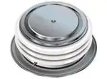
• International standard case K-PUK (A-24)
• High profile hockey PUK
• Material categorization: for definitions of compliance
please see www.vishay.com/doc?99912
TYPICAL APPLICATIONS
K-PUK (A-24)
• DC motor controls
PRIMARY CHARACTERISTICS
• Controlled DC power supplies
IT(AV)
1473 A
VDRM/VRRM
1200 V, 1400 V, 1600 V, 1800 V,
2000 V, 2200 V, 2400 V
VTM
1.80 V
IGT
100 mA
TJ
-40 °C to +125 °C
Package
K-PUK (A-24)
Circuit configuration
Single SCR
• AC controllers
MAJOR RATINGS AND CHARACTERISTICS
PARAMETER
TEST CONDITIONS
IT(AV)
Ths
IT(RMS)
Ths
ITSM
VALUES
UNITS
1473
A
55
°C
2913
A
25
°C
50 Hz
20.0
60 Hz
21.2
A
50 Hz
2000
60 Hz
1865
VDRM/VRRM
Range
1200 to 2400
V
tq
Typical
300
μs
TJ
Range
-40 to +125
°C
IRRM MAXIMUM
AT TJ = 125 °C
mA
I2t
I2t
20 000
kA2s
kA2s
ELECTRICAL SPECIFICATIONS
VOLTAGE RATINGS
TYPE NUMBER
VS-ST1000C..K
VOLTAGE
CODE
VRRM, MAXIMUM REPETITIVE PEAK
REVERSE VOLTAGE
V
VRSM, MAXIMUM
NON-REPETITIVE PEAK REVERSE
VOLTAGE
V
12
1200
1300
14
1400
1500
16
1600
1700
18
1800
1900
20
2000
2100
22
2200
2300
24
2400
2500
100
Revision: 21-Sep-17
Document Number: 93714
1
For technical questions within your region: DiodesAmericas@vishay.com, DiodesAsia@vishay.com, DiodesEurope@vishay.com
THIS DOCUMENT IS SUBJECT TO CHANGE WITHOUT NOTICE. THE PRODUCTS DESCRIBED HEREIN AND THIS DOCUMENT
ARE SUBJECT TO SPECIFIC DISCLAIMERS, SET FORTH AT www.vishay.com/doc?91000
�VS-ST1000C..K Series
www.vishay.com
Vishay Semiconductors
ABSOLUTE MAXIMUM RATINGS
PARAMETER
SYMBOL
Maximum average on-state current
at heatsink temperature
Maximum RMS on-state current
Maximum peak, one-cycle,
non-repetitive surge current
IT(AV)
IT(RMS)
ITSM
TEST CONDITIONS
A
55 (85)
°C
DC at 25 °C heatsink temperature double side cooled
6540
A
t = 10 ms
20.0
t = 8.3 ms
t = 10 ms
t = 8.3 ms
I2t
t = 8.3 ms
Maximum
for fusing
I2t
No voltage
reapplied
100 % VRRM
reapplied
No voltage
reapplied
21.2
17.0
Sinusoidal half wave,
initial TJ = TJ maximum
18.1
1865
1445
t = 0.1 ms to 10 ms, no voltage reapplied
20 000
VT(TO)1
(16.7 % x x IT(AV) < I < x IT(AV)), TJ = TJ maximum
0.950
High level value of threshold voltage
VT(TO)2
(I > x IT(AV)), TJ = TJ maximum
1.024
Low level value of on-state slope resistance
rt1
(16.7 % x x IT(AV) < I < x IT(AV)), TJ = TJ maximum
0.283
High level value of on-state slope resistance
rt2
(I > x IT(AV)), TJ = TJ maximum
0.265
Ipk = 3000 A, TJ = 125 °C, tp = 10 ms sine pulse
1.80
VTM
Maximum holding current
IH
Typical latching current
IL
TJ = 25 °C, anode supply 12 V resistive load
kA2s
1360
Low level value of threshold voltage
Maximum on-state voltage drop
kA
2000
100 % VRRM
reapplied
t = 10 ms
t = 8.3 ms
I2t
UNITS
1473 (630)
180° conduction, half sine wave
Double side (single side) cooled
t = 10 ms
Maximum I2t for fusing
VALUES
600
1000
kA2s
V
m
V
mA
SWITCHING
PARAMETER
Maximum non-repetitive rate of
rise of turned-on current
SYMBOL
dI/dt
TEST CONDITIONS
Gate drive 20 V, 20 , tr 1 μs
TJ = TJ maximum, anode voltage 80 % VDRM
VALUES
UNITS
1000
A/μs
Typical delay time
td
Gate current 1 A, dIg/dt = 1 A/μs
Vd = 0.67 % VDRM, TJ = 25 °C
1.9
Typical turn-off time
tq
ITM = 550 A, TJ = TJ maximum, dI/dt = 40 A/μs,
VR = 50 V, dV/dt = 20 V/μs, gate 0 V 100 , tp = 500 μs
300
SYMBOL
TEST CONDITIONS
VALUES
UNITS
μs
BLOCKING
PARAMETER
Maximum critical rate of rise of
off-state voltage
dV/dt
TJ = TJ maximum linear to 80 % rated VDRM
500
V/μs
Maximum peak reverse and
off-state leakage current
IRRM,
IDRM
TJ = TJ maximum, rated VDRM/VRRM applied
100
mA
Revision: 21-Sep-17
Document Number: 93714
2
For technical questions within your region: DiodesAmericas@vishay.com, DiodesAsia@vishay.com, DiodesEurope@vishay.com
THIS DOCUMENT IS SUBJECT TO CHANGE WITHOUT NOTICE. THE PRODUCTS DESCRIBED HEREIN AND THIS DOCUMENT
ARE SUBJECT TO SPECIFIC DISCLAIMERS, SET FORTH AT www.vishay.com/doc?91000
�VS-ST1000C..K Series
www.vishay.com
Vishay Semiconductors
TRIGGERING
PARAMETER
SYMBOL
Maximum peak gate power
PGM
Maximum peak average gate power
PG(AV)
Maximum peak positive gate current
IGM
Maximum peak positive gate voltage
+VGM
Maximum peak negative gate voltage
-VGM
DC gate current required to trigger
IGT
TJ = TJ maximum, f = 50 Hz, d% = 50
3
TJ = TJ maximum, tp 5 ms
W
A
20
V
5.0
TJ = -40 °C
200
-
TJ = 25 °C
100
200
50
-
Maximum required gate trigger/
current/voltage are the lowest
value which will trigger all units
12 V anode to cathode applied
TJ = 25 °C
IGD
TJ = TJ maximum
DC gate voltage not to trigger
UNITS
3.0
TJ = 125 °C
DC gate current not to trigger
MAX.
16
TJ = -40 °C
VGT
TYP.
TJ = TJ maximum, tp 5 ms
TJ = 125 °C
DC gate voltage required to trigger
VALUES
TEST CONDITIONS
VGD
Maximum gate current/voltage
not to trigger is the maximum
value which will not trigger any
unit with rated VDRM anode to
cathode applied
1.4
-
1.1
3.0
0.9
-
mA
V
10
mA
0.25
V
VALUES
UNITS
THERMAL AND MECHANICAL SPECIFICATIONS
PARAMETER
SYMBOL
Maximum operating temperature range
Maximum storage temperature range
TEST CONDITIONS
TJ
-40 to +125
TStg
-40 to +150
Maximum thermal resistance,
junction to heatsink
RthJ-hs
Maximum thermal resistance,
case to heatsink
RthC-hs
DC operation single side cooled
0.042
DC operation double side cooled
0.021
DC operation single side cooled
0.006
DC operation double side cooled
0.003
Mounting force, ± 10 %
Approximate weight
Case style
See dimensions - link at the end of datasheet
°C
K/W
24 500
(2500)
N
(kg)
425
g
K-PUK (A-24)
RthJC CONDUCTION
CONDUCTION ANGLE
SINUSOIDAL CONDUCTION
SINGLE SIDE
DOUBLE SIDE
RECTANGULAR CONDUCTION
SINGLE SIDE
DOUBLE SIDE
180°
0.003
0.003
0.002
0.002
120°
0.004
0.004
0.004
0.004
90°
0.005
0.005
0.005
0.005
60°
0.007
0.007
0.007
0.007
30°
0.012
0.012
0.012
0.012
TEST CONDITIONS
UNITS
TJ = TJ maximum
K/W
Note
• The table above shows the increment of thermal resistance RthJC when devices operate at different conduction angles than DC
Revision: 21-Sep-17
Document Number: 93714
3
For technical questions within your region: DiodesAmericas@vishay.com, DiodesAsia@vishay.com, DiodesEurope@vishay.com
THIS DOCUMENT IS SUBJECT TO CHANGE WITHOUT NOTICE. THE PRODUCTS DESCRIBED HEREIN AND THIS DOCUMENT
ARE SUBJECT TO SPECIFIC DISCLAIMERS, SET FORTH AT www.vishay.com/doc?91000
�VS-ST1000C..K Series
ST1000C..K series
( single side cooled)
R thJ-hs (DC ) = 0.042 K/W
120
110
Conduction Angle
100
90
30°
60°
90°
120°
80
180°
70
0
100
200
300
400
500
600
700
Maximum Allowable Heatsink Temperature (°C)
130
Vishay Semiconductors
130
ST1000C..K series
(double side cooled)
R thJ-hs (DC) = 0.021 K/W
120
110
100
90
Conduction Period
80
30˚
60˚
70
90˚
120˚
60
180˚
50
DC
40
0
400
800
1200
1600
2000
2400
Average On-State Current (A)
Fig. 1 - Current Ratings Characteristics
Fig. 4 - Current Ratings Characteristics
130
ST1000C..K Series
( single side cooled)
R thJ-hs (DC ) = 0.042 K/W
120
110
Conduction Period
100
90
30°
60°
90°
80
120°
180°
DC
70
0
200
400
600
800
1000
Maximum Average On-State Power Loss (W)
Average On-State Current (A)
3000
180˚
120˚
90˚
60˚
30˚
2500
2000
RMS limit
1500
1000
Conduction Angle
ST1000C..K series
TJ = 125˚C
500
0
0
400
800
1200
1600
Average On-State Current (A)
Average On-State Current (A)
Fig. 2 - Current Ratings Characteristics
Fig. 5 - On-State Power Loss Characteristics
130
ST1000C..K Series
(double side cooled)
R thJ-hs (DC) = 0.021 K/W
120
110
100
90
Conduction Angle
30˚
80
60˚
90˚
70
120˚
60
180˚
50
40
0
400
800
1200
1600
Maximum Average On-State Power Loss (W)
Maximum Allowable Heatsink Temperature (°C)
Maximum Allowable Heatsink Temperature (°C)
Maximum Allowable Heatsink Temperature (°C)
www.vishay.com
4000
DC
180˚
120˚
90˚
60˚
30˚
3500
3000
2500
RMS limit
2000
1500
Conduction period
1000
ST1000C..K series
TJ = 125 ˚C
500
0
0
500
1000
1500
2000
2500
Average On-State Current (A)
Average On-State Current (A)
Fig. 3 - Current Ratings Characteristics
Fig. 6 - On-State Power Loss Characteristics
Revision: 21-Sep-17
Document Number: 93714
4
For technical questions within your region: DiodesAmericas@vishay.com, DiodesAsia@vishay.com, DiodesEurope@vishay.com
THIS DOCUMENT IS SUBJECT TO CHANGE WITHOUT NOTICE. THE PRODUCTS DESCRIBED HEREIN AND THIS DOCUMENT
ARE SUBJECT TO SPECIFIC DISCLAIMERS, SET FORTH AT www.vishay.com/doc?91000
�VS-ST1000C..K Series
18 000
Vishay Semiconductors
Peak Half Sine Wave On-state Current (A)
Peak Half Sine Wave On-state Current (A)
www.vishay.com
At any rated load condition and with
rated VRRM applied following surge.
Initial TJ = 125 ˚C
16 000
at 60 Hz 0.0083 s
at 50 Hz 0.0100 s
14 000
12 000
10 000
8000
ST1000C..K series
6000
1
10
22 000
Maximum non repetitive surge current
vs. pulse train duration.
Control of conduction may not be maintained.
Initial TJ = 125 °C
No voltage reapplied
Rated VRRM reapplied
20 000
18 000
16 000
14 000
12 000
10 000
8000
ST1000C..K series
6000
0.01
100
0.1
1
Pulse Train Duration (s)
Number Of Equal Amplitude Half Cycle Current Pulses (N)
Fig. 7 - Maximum Non-Repetitive Surge Current
Single and Double Side Cooled
Fig. 8 - Maximum Non-Repetitive Surge Current
Single and Double Side Cooled
Instantaneous On-State Current (A)
10 000
TJ = 25 ˚C
TJ = 125 ˚C
1000
ST1000C..K series
100
0.5
1
1.5
2
2.5
3
3.5
4
Instantaneous On-State Voltage (V)
Transient Thermal Impedance Z thJ-hs (K/W)
Fig. 9 - On-State Voltage Drop Characteristics
0.1
Steady state value
R thJ-hs = 0.42 K/W
(single side cooled)
R thJ-hs = 0.21 K/W
(double side cooled)
0.01
(DC operation)
0.001
0.001
ST1000C..K series
0.01
0.1
1
10
100
Square Wave Pulse Duration (s)
Fig. 10 - Thermal Impedance ZthJ-hs Characteristics
Revision: 21-Sep-17
Document Number: 93714
5
For technical questions within your region: DiodesAmericas@vishay.com, DiodesAsia@vishay.com, DiodesEurope@vishay.com
THIS DOCUMENT IS SUBJECT TO CHANGE WITHOUT NOTICE. THE PRODUCTS DESCRIBED HEREIN AND THIS DOCUMENT
ARE SUBJECT TO SPECIFIC DISCLAIMERS, SET FORTH AT www.vishay.com/doc?91000
�VS-ST1000C..K Series
www.vishay.com
(1) PGM = 16 W, tp = 4 ms
(2) PGM = 30 W, tp = 2 ms
(3) PGM = 60 W, tp = 1 ms
Rectangular gate pulse
a) Recommended load line for
rated di/dt : 20 V, 10 Ω; tr ± 1 µs
b) Recommended load line for
>= 30 % rated di/dt : 10 V, 10 Ω
tr