VS-ST303C Series
www.vishay.com
Vishay Semiconductors
Inverter Grade Thyristors
(PUK Version), 620 A
FEATURES
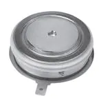
• Metal case with ceramic insulator
• All diffused design
• Center amplifying gate
• Guaranteed high dV/dt
• Guaranteed high dI/dt
• International standard case E-PUK (TO-200AB)
• High surge current capability
E-PUK (TO-200AB)
• Low thermal impedance
• High speed performance
PRIMARY CHARACTERISTICS
Package
E-PUK (TO-200AB)
Circuit configuration
Single SCR
• Designed and qualified for industrial level
• Material categorization: for definitions of compliance
please see www.vishay.com/doc?99912
IT(AV)
620 A
VDRM/VRRM
400 V, 800 V, 1000 V, 1200 V
VTM
2.16 V
ITSM at 50 Hz
7950 A
ITSM at 60 Hz
8320 A
IGT
200 mA
TC/Ths
55 °C
TYPICAL APPLICATIONS
• Inverters
• Choppers
• Induction heating
• All types of force-commutated converters
MAJOR RATINGS AND CHARACTERISTICS
PARAMETER
TEST CONDITIONS
IT(AV)
Ths
IT(RMS)
Ths
ITSM
I2t
A
55
°C
1180
A
25
°C
7950
60 Hz
8320
50 Hz
316
60 Hz
289
Range
TJ
UNITS
620
50 Hz
VDRM/VRRM
tq
VALUES
A
kA2s
400 to 1200
V
10 to 30
μs
-40 to 125
°C
Note
• tq = 10 μs to 20 μs for 400 V to 800 V devices
tq = 15 μs to 30 μs for 1000 V to 1200 V devices
ELECTRICAL SPECIFICATIONS
VOLTAGE RATINGS
TYPE NUMBER
VS-ST303C..C
VOLTAGE
CODE
VDRM/VRRM, MAXIMUM
REPETITIVE PEAK VOLTAGE
V
VRSM, MAXIMUM
NON-REPETITIVE PEAK VOLTAGE
V
04
400
500
08
800
900
10
1000
1100
12
1200
1300
IDRM/IRRM MAXIMUM
AT TJ = TJ MAXIMUM
mA
50
Revision: 28-Aug-17
Document Number: 94373
1
For technical questions within your region: DiodesAmericas@vishay.com, DiodesAsia@vishay.com, DiodesEurope@vishay.com
THIS DOCUMENT IS SUBJECT TO CHANGE WITHOUT NOTICE. THE PRODUCTS DESCRIBED HEREIN AND THIS DOCUMENT
ARE SUBJECT TO SPECIFIC DISCLAIMERS, SET FORTH AT www.vishay.com/doc?91000
�VS-ST303C Series
www.vishay.com
Vishay Semiconductors
CURRENT CARRYING CAPABILITY
ITM
FREQUENCY
ITM
ITM
180° el
UNITS
100 µs
180° el
50 Hz
1314
1130
2070
1940
6930
400 Hz
1260
1040
2190
1880
3440
2960
1000 Hz
900
700
1900
1590
1850
1540
2500 Hz
340
230
910
710
740
Recovery voltage Vr
Voltage before turn-on Vd
50
50
VDRM
VDRM
VDRM
50
-
40
55
Equivalent values for RC circuit
40
10/0.47
A
560
50
Rise of on-state current dI/dt
Heatsink temperature
6270
V
55
40
10/0.47
A/µs
55
°C
/µF
10/0.47
ON-STATE CONDUCTION
PARAMETER
SYMBOL
Maximum average on-state current
at heatsink temperature
IT(AV)
Maximum RMS on-state current
IT(RMS)
Maximum peak, one half cycle,
non-repetitive surge current
ITSM
TEST CONDITIONS
180° conduction, half sine wave
double side (single side) cooled
1180
7950
t = 10 ms
t = 10 ms
I2t
t = 8.3 ms
t = 10 ms
t = 8.3 ms
Maximum I2t for fusing
I2t
Maximum peak on-state voltage
VTM
A
°C
t = 10 ms
t = 8.3 ms
No voltage
reapplied
100 % VRRM
reapplied
No voltage
reapplied
UNITS
55 (85)
DC at 25 °C heatsink temperature double side cooled
t = 8.3 ms
Maximum I2t for fusing
VALUES
620 (230)
8320
A
6690
Sinusoidal half wave,
initial TJ = TJ maximum
100 % VRRM
reapplied
t = 0.1 to 10 ms, no voltage reapplied
7000
316
289
224
kA2s
204
3160
ITM = 1255 A, TJ = TJ maximum,
tp = 10 ms sine wave pulse
2.16
Low level value of threshold voltage
VT(TO)1
(16.7 % x x IT(AV) < I < x IT(AV)), TJ = TJ maximum
1.44
High level value of threshold voltage
VT(TO)2
(I > x IT(AV)), TJ = TJ maximum
1.48
Low level value of forward slope resistance
rt1
(16.7 % x x IT(AV) < I < x IT(AV)), TJ = TJ maximum
0.57
High level value of forward slope
resistance
rt2
(I > x IT(AV)), TJ = TJ maximum
0.56
Maximum holding current
IH
TJ = 25 °C, IT > 30 A
600
Typical latching current
IL
TJ = 25 °C, VA = 12 V, Ra = 6 , IG = 1 A
1000
klA2s
V
m
mA
SWITCHING
PARAMETER
SYMBOL
Maximum non-repetitive rate of rise
of turned on current
Typical delay time
VALUES
UNITS
TJ = TJ maximum, VDRM = Rated VDRM
ITM = 2 x dI/dt
1000
A/μs
td
TJ = 25 °C, VDM = Rated VDRM, ITM = 50 A DC, tp = 1 μs
Resistive load, gate pulse: 10 V, 5 source
0.83
tq
TJ = TJ maximum,
ITM = 550 A, commutating dI/dt = 40 A/μs
VR = 50 V, tp = 500 μs, dV/dt: see table in device code
dI/dt
minimum
Maximum turn-off time (1)
maximum
TEST CONDITIONS
10
μs
30
Note
(1) t = 10 μs to 20 μs for 400 V to 800 V devices; t = 15 μs to 30 μs for 1000 V to 1200 V devices
q
q
Revision: 28-Aug-17
Document Number: 94373
2
For technical questions within your region: DiodesAmericas@vishay.com, DiodesAsia@vishay.com, DiodesEurope@vishay.com
THIS DOCUMENT IS SUBJECT TO CHANGE WITHOUT NOTICE. THE PRODUCTS DESCRIBED HEREIN AND THIS DOCUMENT
ARE SUBJECT TO SPECIFIC DISCLAIMERS, SET FORTH AT www.vishay.com/doc?91000
�VS-ST303C Series
www.vishay.com
Vishay Semiconductors
BLOCKING
PARAMETER
SYMBOL
TEST CONDITIONS
VALUES
UNITS
500
V/µs
Maximum critical rate of rise of off-state voltage
dV/dt
TJ = TJ maximum, linear to 80 % VDRM,
higher value available on request
Maximum peak reverse and off-state leakage current
IRRM,
IDRM
TJ = TJ maximum, rated VDRM/VRRM applied
50
mA
SYMBOL
TEST CONDITIONS
VALUES
UNITS
TRIGGERING
PARAMETER
PGM
Maximum peak gate power
PG(AV)
Maximum average gate power
Maximum peak positive gate current
IGM
Maximum peak positive gate voltage
+ VGM
Maximum peak negative gate voltage
- VGM
Maximum DC gate current required to trigger
IGT
Maximum DC gate voltage required to trigger
VGT
Maximum DC gate current not to trigger
IGD
Maximum DC gate voltage not to trigger
VGD
60
TJ = TJ maximum, f = 50 Hz, d% = 50
10
10
TJ = TJ maximum, tp 5 ms
20
5
TJ = 25 °C, VA = 12 V, Ra = 6
TJ = TJ maximum, rated VDRM applied
W
A
V
200
mA
3
V
20
mA
0.25
V
VALUES
UNITS
THERMAL AND MECHANICAL SPECIFICATIONS
PARAMETER
SYMBOL
Maximum operating junction temperature range
Maximum storage temperature range
Maximum thermal resistance, junction to heatsink
Maximum thermal resistance, case to heatsink
TEST CONDITIONS
TJ
-40 to 125
TStg
-40 to 150
RthJ-hs
RthC-hs
DC operation single side cooled
0.09
DC operation double side cooled
0.04
DC operation single side cooled
0.020
DC operation double side cooled
0.010
Mounting force, ± 10 %
Approximate weight
Case style
°C
See dimensions - link at the end of datasheet
K/W
9800
(1000)
N
(kg)
83
g
E-PUK (TO-200AB)
RthJ-hs CONDUCTION
CONDUCTION ANGLE
SINUSOIDAL CONDUCTION
SINGLE SIDE
DOUBLE SIDE
RECTANGULAR CONDUCTION
SINGLE SIDE
DOUBLE SIDE
180°
0.010
0.010
0.007
0.007
120°
0.012
0.012
0.012
0.013
90°
0.015
0.015
0.016
0.017
60°
0.022
0.022
0.023
0.023
30°
0.036
0.036
0.036
0.037
TEST CONDITIONS
UNITS
TJ = TJ max.
K/W
Note
• The table above shows the increment of thermal resistance RthJ-hs when devices operate at different conduction angles than DC
Revision: 28-Aug-17
Document Number: 94373
3
For technical questions within your region: DiodesAmericas@vishay.com, DiodesAsia@vishay.com, DiodesEurope@vishay.com
THIS DOCUMENT IS SUBJECT TO CHANGE WITHOUT NOTICE. THE PRODUCTS DESCRIBED HEREIN AND THIS DOCUMENT
ARE SUBJECT TO SPECIFIC DISCLAIMERS, SET FORTH AT www.vishay.com/doc?91000
�VS-ST303C Series
www.vishay.com
Vishay Semiconductors
ST303C..C Series
(Single side cooled)
RthJ-hs (DC) = 0.09 K/W
120
110
130
100
Ø
90
Conduction angle
80
70
180°
60
30°
50
60°
ST303C..C Series
(Double side cooled)
RthJ-hs (DC) = 0.04 K/W
120
90°
120°
Maximum Allowable
Heatsink Temperature (°C)
Maximum Allowable
Heatsink Temperature (°C)
130
110
100
90
Ø
80
Conduction period
70
60
50
DC
40
180°
30
40
0
100
50
150
200
250
300
350
400
60°
30°
90° 120°
20
0
Average On-State Current (A)
200
400
600
1000
800
1200
Average On-State Current (A)
Fig. 1 - Current Ratings Characteristics
Fig. 4 - Current Ratings Characteristics
130
ST303C..C Series
(Single side cooled)
RthJ-hs (DC) = 0.09 K/W
110
2000
Maximum Average On-State
Power Loss (W)
Maximum Allowable
Heatsink Temperature (°C)
120
100
90
Ø
80
Conduction period
70
60
50
60°
40
30°
DC
90°
30
180°
120°
20
0
100
200
400
300
500
600
700
180°
120°
90°
60°
30°
1800
1600
1400
1200
RMS limit
1000
800
Ø
600
Conduction angle
400
ST303C..C Series
TJ = 125 °C
200
0
0
Average On-State Current (A)
100
200
300
400
500
600
700
800
Average On-State Current (A)
Fig. 2 - Current Ratings Characteristics
Fig. 5 - On-State Power Loss Characteristics
130
110
100
90
Ø
Conduction angle
80
70
60
50
180°
40
30
30°
60°
90°
120°
500
600
20
0
100
200
300
400
700
Average On-State Current (A)
Fig. 3 - Current Ratings Characteristics
800
Maximum Average On-State
Power Loss (W)
Maximum Allowable
Heatsink Temperature (°C)
2800
ST303C..C Series
(Double side cooled)
RthJ-hs (DC) = 0.04 K/W
120
DC
180°
120°
90°
60°
30°
2400
2000
1600
RMS limit
1200
Ø
800
Conduction period
400
ST303C..C Series
TJ = 125 °C
0
0
200
400
600
800
1000
1200
Average On-State Current (A)
Fig. 6 - On-State Power Loss Characteristics
Revision: 28-Aug-17
Document Number: 94373
4
For technical questions within your region: DiodesAmericas@vishay.com, DiodesAsia@vishay.com, DiodesEurope@vishay.com
THIS DOCUMENT IS SUBJECT TO CHANGE WITHOUT NOTICE. THE PRODUCTS DESCRIBED HEREIN AND THIS DOCUMENT
ARE SUBJECT TO SPECIFIC DISCLAIMERS, SET FORTH AT www.vishay.com/doc?91000
�VS-ST303C Series
www.vishay.com
Vishay Semiconductors
1
7500
ZthJ-hs - Transient Thermal
Impedance (K/W)
7000
Peak Half Sine Wave
On-State Current (A)
ST303C..C Series
At any rated load condition and with
rated VRRM applied following surge
Initial TJ = 125 °C
at 60 Hz 0.0083 s
at 50 Hz 0.0100 s
6500
6000
5500
5000
4500
4000
3500
ST303C..C Series
Steady state value
RthJ-hs = 0.09 K/W
(Single side cooled)
RthJ-hs = 0.04 K/W
(Double side cooled)
(DC operation)
0.01
0.001
0.001
3000
1
0.1
10
0.01
0.1
1
10
100
Square Wave Pulse Duration (s)
Number of Equal Amplitude Half Cycle
Current Pulses (N)
Fig. 10 - Thermal Impedance ZthJ-hs Characteristics
8000
Maximum non-repetitive surge current
versus pulse train duration. Control of
conduction may not be maintained
Initial TJ = 125 °C
No voltage reapplied
Rated VRRM reapplied
Peak Half Sine Wave
On-State Current (A)
7500
7000
6500
6000
5500
5000
4500
4000
3500
ST303C..C Series
3000
0.01
0.1
1
Pulse Train Duration (s)
Qrr - Maximum Reverse Recovery Charge (µC)
Fig. 7 - Maximum Non-Repetitive Surge Current
Single and Double Side Cooled
ITM = 500 A
ITM = 300 A
ITM = 200 A
ITM = 100 A
ITM = 50 A
300
280
260
240
220
200
180
160
140
120
ST303C..C Series
TJ = 125 °C
100
80
10
20
30
40
50
60
70
80
90
100
dI/dt - Rate of Fall of On-State Current (A/µs)
Fig. 11 - Reverse Recovered Charge Characteristics
Fig. 8 - Maximum Non-Repetitive Surge Current
Single and Double Side Cooled
10 000
1000
TJ = 25 °C
TJ = 125 °C
ST303C..C Series
100
0
1
2
3
4
5
6
7
Instantaneous On-State Voltage (V)
Fig. 9 - On-State Voltage Drop Characteristics
8
Irr - Maximum Reverse Recovery Current (A)
Instantaneous On-State Current (A)
320
180
ITM = 500 A
ITM = 300 A
ITM = 200 A
ITM = 100 A
ITM = 50 A
160
140
120
100
80
ST303C..C Series
TJ = 125 °C
60
40
20
10
20
30
40
50
60
70
80
90
100
dI/dt - Rate of Fall of Forward Current (A/µs)
Fig. 12 - Reverse Recovered Current Characteristics
Revision: 28-Aug-17
Document Number: 94373
5
For technical questions within your region: DiodesAmericas@vishay.com, DiodesAsia@vishay.com, DiodesEurope@vishay.com
THIS DOCUMENT IS SUBJECT TO CHANGE WITHOUT NOTICE. THE PRODUCTS DESCRIBED HEREIN AND THIS DOCUMENT
ARE SUBJECT TO SPECIFIC DISCLAIMERS, SET FORTH AT www.vishay.com/doc?91000
�VS-ST303C Series
www.vishay.com
Vishay Semiconductors
10 000
400
50 Hz
200
100
500
1000
Snubber circuit
Rs = 10 Ω
Cs = 0.47 µF
VD = 80 % VDRM
1500
1000
2000
2500
3000
tp
ST303C..C Series
Sinusoidal pulse
TC = 40 °C
Peak On-State Current (A)
Peak On-State Current (A)
10 000
200
400
50 Hz
100
500
1000
Snubber circuit
Rs = 10 Ω
Cs = 0.47 µF
VD = 80 % VDRM
1000
1500
2000
2500
ST303C..C Series
Sinusoidal pulse
TC = 55 °C
3000
tp
100
100
10
100
1000
10 000
10
100
Pulse Basewidth (µs)
1000
10 000
Pulse Basewidth (µs)
Fig. 13 - Frequency Characteristics
10 000
Snubber circuit
Rs = 10 Ω
Cs = 0.47 µF
VD = 80 % VDRM
200
500
50 Hz
100
400
1000
1000
1500
2000
2500
3000
tp
ST303C..C Series
Trapezoidal pulse
TC = 40 °C
dI/dt = 50 A/µs
Peak On-State Current (A)
Peak On-State Current (A)
10 000
100
1000
50 Hz
200
100
500
400
1000
1000
1500
2000
2500
10 000
tp
3000
100
100
10
Snubber circuit
Rs = 10 Ω
Cs = 0.47 µF
VD = 80 % VDRM
10
100
Pulse Basewidth (µs)
ST303C..C Series
Trapezoidal pulse
TC = 55 °C
dI/dt = 50 A/µs
1000
10 000
Pulse Basewidth (µs)
Fig. 14 - Frequency Characteristics
10 000
Snubber circuit
Rs = 10 Ω
Cs = 0.47 µF
VD = 80 % VDRM
50 Hz
200
500
400
100
1000
1000
1500
2000
2500
3000
tp
ST303C..C Series
Trapezoidal pulse
TC = 40 °C
dI/dt = 100 A/µs
100
10
100
1000
Peak On-State Current (A)
Peak On-State Current (A)
10 000
Snubber circuit
Rs = 10 Ω
Cs = 0.47 µF
VD = 80 % VDRM
50 Hz
400
200
100
500
1000
1000
1500
2000
2500
100
10 000
Pulse Basewidth (µs)
tp
3000
10
100
ST303C..C Series
Trapezoidal pulse
TC = 55 °C
dI/dt = 100 A/µs
1000
10 000
Pulse Basewidth (µs)
Fig. 15 - Frequency Characteristics
Revision: 28-Aug-17
Document Number: 94373
6
For technical questions within your region: DiodesAmericas@vishay.com, DiodesAsia@vishay.com, DiodesEurope@vishay.com
THIS DOCUMENT IS SUBJECT TO CHANGE WITHOUT NOTICE. THE PRODUCTS DESCRIBED HEREIN AND THIS DOCUMENT
ARE SUBJECT TO SPECIFIC DISCLAIMERS, SET FORTH AT www.vishay.com/doc?91000
�VS-ST303C Series
www.vishay.com
Vishay Semiconductors
100 000
Peak On-State Current (A)
Peak On-State Current (A)
100 000
20 joules per pulse
10 000
10
3
5
2
1
1000
0.5
0.4
100
ST303C..C Series
Sinusoidal pulse
ST303C..C Series
Rectangular pulse
dI/dt = 50 A/µs
tp
10 000
20 joules per pulse
3
1000
10
5
2
1
0.5
100
0.4
tp
10
10
10
100
1000
10 000
10
100
Pulse Basewidth (µs)
1000
10 000
Pulse Basewidth (µs)
Fig. 16 - Maximum On-State Energy Power Loss Characteristics
10
(1) PGM = 10 W,
(2) PGM = 20 W,
(3) PGM = 40 W,
(4) PGM = 60 W,
Rectangular gate pulse
a) Recommended load line for
rated dI/dt: 20 V, 10 Ω; tr ≤ 1 µs
b) Recommended load line for
≤ 30 % rated dI/dt: 10 V, 10 Ω
tr ≤ 1 µs
TJ = 40 °C
(b)
TJ = 25 °C
1
tp = 20 ms
tp = 10 ms
tp = 5 ms
tp = 3.3 ms
(a)
TJ = 125 °C
Instantaneous Gate Voltage (V)
100
(1)
(2)
(3) (4)
VGD
IGD
0.1
0.001
0.01
Device: ST303C..C Series
0.1
1
Frequency limited by PG(AV)
10
100
Instantaneous Gate Current (A)
Fig. 17 - Gate Characteristics
Revision: 28-Aug-17
Document Number: 94373
7
For technical questions within your region: DiodesAmericas@vishay.com, DiodesAsia@vishay.com, DiodesEurope@vishay.com
THIS DOCUMENT IS SUBJECT TO CHANGE WITHOUT NOTICE. THE PRODUCTS DESCRIBED HEREIN AND THIS DOCUMENT
ARE SUBJECT TO SPECIFIC DISCLAIMERS, SET FORTH AT www.vishay.com/doc?91000
�VS-ST303C Series
www.vishay.com
Vishay Semiconductors
ORDERING INFORMATION TABLE
Device code
VS-
ST
30
3
C
12
C
H
K
1
-
1
2
3
4
5
6
7
8
9
10
11
1
-
Vishay Semiconductors product
2
-
Thyristor
3
-
Essential part number
4
-
3 = fast turn-off
5
-
C = ceramic PUK
6
-
Voltage code x 100 = VRRM
(see Voltage Ratings table)
7
-
8
-
9
-
10
-
dV/dt - tq combinations available
dV/dt (V/μs) 20 50 100 200
CN DN EN FN*
10
tq (μs)
C = PUK case E-PUK (TO-200AB)
CM DM EM FM
12
up to 800 V
15
CL DL EL FL*
Reapplied dV/dt code (for tq test condition)
20
CK DK EK FK*
tq code
CL 15
tq (μs)
CP DP 18
0 = eyelet terminals
20
CK DK EK FK*
only
for
(gate and aux. cathode unsoldered leads)
CJ DJ EJ FJ*
1000 V/1200 V 25
- DH EH FH
30
1 = fast-on terminals
(gate and aux. cathode unsoldered leads) * Standard part number.
All other types available only on request.
2 = eyelet terminals
400
HN
HM
HL
HK
HK
HJ
HH
(gate and aux. cathode soldered leads)
3 = fast-on terminals
(gate and aux. cathode soldered leads)
11
-
Critical dV/dt:
None = 500 V/μs (standard value)
L = 1000 V/μs (special selection)
LINKS TO RELATED DOCUMENTS
Dimensions
http://www.vishay.com/doc?95075
Revision: 28-Aug-17
Document Number: 94373
8
For technical questions within your region: DiodesAmericas@vishay.com, DiodesAsia@vishay.com, DiodesEurope@vishay.com
THIS DOCUMENT IS SUBJECT TO CHANGE WITHOUT NOTICE. THE PRODUCTS DESCRIBED HEREIN AND THIS DOCUMENT
ARE SUBJECT TO SPECIFIC DISCLAIMERS, SET FORTH AT www.vishay.com/doc?91000
�Outline Dimensions
www.vishay.com
Vishay Semiconductors
E-PUK (TO-200AB)
DIMENSIONS in millimeters (inches)
Anode to gate
Creepage distance: 11.18 (0.44) minimum
Strike distance: 7.62 (0.30) minimum
25.3 (0.99)
DIA. MAX.
0.3 (0.01) MIN.
C
G
14.1/15.1
(0.56/0.59)
A
0.3 (0.01) MIN.
25.3 (0.99)
DIA. MAX.
Gate terminal for
1.47 (0.06) DIA.
pin receptacle
Note:
A = Anode
C = Cathode
G = Gate
40.5 (1.59) DIA. MAX.
2 holes 3.56 (0.14) x 1.83 (0.07) minimum deep
6.5 (0.26)
4.75 (0.19)
25° ± 5°
42 (1.65) MAX.
28 (1.10)
Quote between upper and lower pole pieces has to be considered after
application of mounting force (see thermal and mechanical specification)
Revision: 12-Jul-17
Document Number: 95075
1
For technical questions within your region: DiodesAmericas@vishay.com, DiodesAsia@vishay.com, DiodesEurope@vishay.com
THIS DOCUMENT IS SUBJECT TO CHANGE WITHOUT NOTICE. THE PRODUCTS DESCRIBED HEREIN AND THIS DOCUMENT
ARE SUBJECT TO SPECIFIC DISCLAIMERS, SET FORTH AT www.vishay.com/doc?91000
�Legal Disclaimer Notice
www.vishay.com
Vishay
Disclaimer
ALL PRODUCT, PRODUCT SPECIFICATIONS AND DATA ARE SUBJECT TO CHANGE WITHOUT NOTICE TO IMPROVE
RELIABILITY, FUNCTION OR DESIGN OR OTHERWISE.
Vishay Intertechnology, Inc., its affiliates, agents, and employees, and all persons acting on its or their behalf (collectively,
“Vishay”), disclaim any and all liability for any errors, inaccuracies or incompleteness contained in any datasheet or in any other
disclosure relating to any product.
Vishay makes no warranty, representation or guarantee regarding the suitability of the products for any particular purpose or
the continuing production of any product. To the maximum extent permitted by applicable law, Vishay disclaims (i) any and all
liability arising out of the application or use of any product, (ii) any and all liability, including without limitation special,
consequential or incidental damages, and (iii) any and all implied warranties, including warranties of fitness for particular
purpose, non-infringement and merchantability.
Statements regarding the suitability of products for certain types of applications are based on Vishay's knowledge of typical
requirements that are often placed on Vishay products in generic applications. Such statements are not binding statements
about the suitability of products for a particular application. It is the customer's responsibility to validate that a particular product
with the properties described in the product specification is suitable for use in a particular application. Parameters provided in
datasheets and / or specifications may vary in different applications and performance may vary over time. All operating
parameters, including typical parameters, must be validated for each customer application by the customer's technical experts.
Product specifications do not expand or otherwise modify Vishay's terms and conditions of purchase, including but not limited
to the warranty expressed therein.
Hyperlinks included in this datasheet may direct users to third-party websites. These links are provided as a convenience and
for informational purposes only. Inclusion of these hyperlinks does not constitute an endorsement or an approval by Vishay of
any of the products, services or opinions of the corporation, organization or individual associated with the third-party website.
Vishay disclaims any and all liability and bears no responsibility for the accuracy, legality or content of the third-party website
or for that of subsequent links.
Except as expressly indicated in writing, Vishay products are not designed for use in medical, life-saving, or life-sustaining
applications or for any other application in which the failure of the Vishay product could result in personal injury or death.
Customers using or selling Vishay products not expressly indicated for use in such applications do so at their own risk. Please
contact authorized Vishay personnel to obtain written terms and conditions regarding products designed for such applications.
No license, express or implied, by estoppel or otherwise, to any intellectual property rights is granted by this document or by
any conduct of Vishay. Product names and markings noted herein may be trademarks of their respective owners.
© 2022 VISHAY INTERTECHNOLOGY, INC. ALL RIGHTS RESERVED
Revision: 01-Jan-2022
1
Document Number: 91000
�