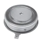
VS-ST380CH Series
www.vishay.com
Vishay Semiconductors
Phase Control Thyristors
(Hockey PUK Version), 960 A
FEATURES
• Center amplifying gate
• Metal case with ceramic insulator
• International standard case E-PUK (TO-200AB)
• Extended temperature range
• Low profile hockey PUK to increase current-carrying
capability
E-PUK (TO-200AB)
• Designed and qualified for industrial level
• Material categorization: for definitions of compliance
please see www.vishay.com/doc?99912
PRIMARY CHARACTERISTICS
IT(AV)
960 A
VDRM/VRRM
400 V, 600 V
VTM
1.58 V
IGT
100 mA
TJ
-40 °C to +150 °C
Package
E-PUK (TO-200AB)
Circuit configuration
Single SCR
TYPICAL APPLICATIONS
• DC motor controls
• Controlled DC power supplies
• AC controllers
MAJOR RATINGS AND CHARACTERISTICS
PARAMETER
TEST CONDITIONS
IT(AV)
Ths
IT(RMS)
Ths
ITSM
I2t
A
80
°C
2220
A
25
°C
12 500
60 Hz
13 000
50 Hz
782
60 Hz
713
Typical
TJ
UNITS
960
50 Hz
VDRM/VRRM
tq
VALUES
A
kA2s
400 to 600
V
100
μs
-40 to 150
°C
ELECTRICAL SPECIFICATIONS
VOLTAGE RATINGS
TYPE NUMBER
VS-ST380CH..C
VOLTAGE
CODE
VDRM/VRRM, MAXIMUM REPETITIVE
PEAK AND OFF-STATE VOLTAGE
V
04
400
500
06
600
700
VRSM, MAXIMUM
IDRM/IRRM MAXIMUM
NON-REPETITIVE PEAK VOLTAGE
AT TJ = TJ
V
MAXIMUM mA
100
Revision: 27-Sep-17
Document Number: 94411
1
For technical questions within your region: DiodesAmericas@vishay.com, DiodesAsia@vishay.com, DiodesEurope@vishay.com
THIS DOCUMENT IS SUBJECT TO CHANGE WITHOUT NOTICE. THE PRODUCTS DESCRIBED HEREIN AND THIS DOCUMENT
ARE SUBJECT TO SPECIFIC DISCLAIMERS, SET FORTH AT www.vishay.com/doc?91000
�VS-ST380CH Series
www.vishay.com
Vishay Semiconductors
ABSOLUTE MAXIMUM RATINGS
PARAMETER
SYMBOL
Maximum average on-state current
at heatsink temperature
Maximum RMS on-state current
IT(AV)
IT(RMS)
TEST CONDITIONS
180° conduction, half sine wave
double side (single side) cooled
DC at 25 °C heatsink temperature double side cooled
t = 10 ms
Maximum peak, one-cycle
non-repetitive surge current
ITSM
t = 8.3 ms
t = 10 ms
t = 8.3 ms
t = 10 ms
Maximum I2t for fusing
I2t
t = 8.3 ms
t = 10 ms
t = 8.3 ms
Maximum
I2t
for fusing
I2t
VALUES
960 (440)
A
80 (110)
°C
2220
12 500
No voltage
reapplied
13 000
100 % VRRM
reapplied
11 000
No voltage
reapplied
Sinusoidal half wave,
initial TJ = TJ maximum
100 % VRRM
reapplied
782
713
553
t = 0.1 to 10 ms, no voltage reapplied
7820
(16.7 % x x IT(AV) < I < x IT(AV)), TJ = TJ maximum
0.85
High level value of threshold voltage
VT(TO)2
(I > x IT(AV)), TJ = TJ maximum
0.88
Low level value of on-state slope resistance
rt1
(16.7 % x x IT(AV) < I < x IT(AV)), TJ = TJ maximum
0.25
High level value of on-state slope resistance
rt2
(I > x IT(AV)), TJ = TJ maximum
0.24
Ipk = 2900 A, TJ = TJ maximum, tp = 10 ms sine pulse
1.58
VTM
IH
Typical latching current
IL
TJ = 25 °C, anode supply 12 V resistive load
kA2s
505
VT(TO)1
Maximum on-state voltage
A
10 500
Low level value of threshold voltage
Maximum holding current
UNITS
600
1000
kA2s
V
m
V
mA
SWITCHING
PARAMETER
Maximum non-repetitive rate of rise
of turned-on current
SYMBOL
dI/dt
TEST CONDITIONS
Gate drive 20 V, 20 , tr 1 μs
TJ = TJ maximum, anode voltage 80 % VDRM
VALUES
UNITS
1000
A/µs
Typical delay time
td
Gate current 1 A, dIg/dt = 1 A/μs
Vd = 0.67 % VDRM, TJ = 25 °C
1.0
Typical turn-off time
tq
ITM = 550 A, TJ = TJ maximum, dI/dt = 40 A/μs,
VR = 50 V, dV/dt = 20 V/μs, gate 0 V 100 , tp = 500 μs
100
SYMBOL
TEST CONDITIONS
VALUES
UNITS
µs
BLOCKING
PARAMETER
Maximum critical rate of rise of
off-state voltage
dV/dt
TJ = TJ maximum linear to 80 % rated VDRM
500
V/µs
Maximum peak reverse and
off-state leakage current
IRRM,
IDRM
TJ = TJ maximum, rated VDRM/VRRM applied
100
mA
Revision: 27-Sep-17
Document Number: 94411
2
For technical questions within your region: DiodesAmericas@vishay.com, DiodesAsia@vishay.com, DiodesEurope@vishay.com
THIS DOCUMENT IS SUBJECT TO CHANGE WITHOUT NOTICE. THE PRODUCTS DESCRIBED HEREIN AND THIS DOCUMENT
ARE SUBJECT TO SPECIFIC DISCLAIMERS, SET FORTH AT www.vishay.com/doc?91000
�VS-ST380CH Series
www.vishay.com
Vishay Semiconductors
TRIGGERING
PARAMETER
SYMBOL
PGM
Maximum peak gate power
PG(AV)
Maximum average gate power
Maximum peak positive gate current
IGM
Maximum peak positive gate voltage
+ VGM
Maximum peak negative gate voltage
- VGM
IGT
DC gate current required to trigger
10.0
TJ = TJ maximum, f = 50 Hz, d% = 50
2.0
TJ = TJ maximum, tp 5 ms
3.0
200
-
TJ = 25 °C
100
200
TJ = 25 °C
IGD
TJ = TJ maximum
VGD
DC gate voltage not to trigger
V
TJ = -40 °C
TJ = 150 °C
DC gate current not to trigger
A
5.0
Maximum required gate trigger/
current/voltage are the lowest
value which will trigger all units
12 V anode to cathode applied
Maximum gate current/voltage
not to trigger is the maximum
value which will not trigger any
unit with rated VDRM anode to
cathode applied
UNITS
W
20
TJ = TJ maximum, tp 5 ms
TJ = 150 °C
VGT
MAX.
TYP.
TJ = TJ maximum, tp 5 ms
TJ = -40 °C
DC gate voltage required to trigger
VALUES
TEST CONDITIONS
40
-
2.5
-
1.8
3.0
1.0
-
mA
V
10
mA
0.25
V
VALUES
UNITS
-40 to 150
°C
THERMAL AND MECHANICAL SPECIFICATIONS
PARAMETER
SYMBOL
Maximum operating junction temperature range
Maximum storage temperature range
Maximum thermal resistance, junction to heatsink
Maximum thermal resistance, case to heatsink
TEST CONDITIONS
TJ
TStg
RthJ-hs
RthC-hs
DC operation single side cooled
0.09
DC operation double side cooled
0.04
DC operation single side cooled
0.02
0.01
DC operation double side cooled
Mounting force, ± 10 %
Approximate weight
Case style
K/W
See dimensions - link at the end of datasheet
9800
(1000)
N
(kg)
83
g
E-PUK (TO-200AB)
RthJ-hs CONDUCTION
CONDUCTION ANGLE
SINUSOIDAL CONDUCTION
RECTANGULAR CONDUCTION
SINGLE SIDE DOUBLE SIDE
SINGLE SIDE
DOUBLE SIDE
180°
0.010
0.011
0.007
0.007
120°
0.012
0.012
0.012
0.013
90°
0.015
0.015
0.016
0.017
60°
0.022
0.022
0.023
0.023
30°
0.036
0.036
0.036
0.037
TEST CONDITIONS
UNITS
TJ = TJ maximum
K/W
Note
• The table above shows the increment of thermal resistance RthJ-hs when devices operate at different conduction angles than DC
Revision: 27-Sep-17
Document Number: 94411
3
For technical questions within your region: DiodesAmericas@vishay.com, DiodesAsia@vishay.com, DiodesEurope@vishay.com
THIS DOCUMENT IS SUBJECT TO CHANGE WITHOUT NOTICE. THE PRODUCTS DESCRIBED HEREIN AND THIS DOCUMENT
ARE SUBJECT TO SPECIFIC DISCLAIMERS, SET FORTH AT www.vishay.com/doc?91000
�VS-ST380CH Series
150
Vishay Semiconductors
ST380CH..C Series
(Single Side Cooled)
RthJ-hs (DC) = 0.09 K/ W
140
130
120
110
Conduc tion Angle
100
90
30°
80
60°
90°
70
120°
60
180°
50
40
0
100 200 300 400 500 600 700 800
Maximum Allowable Heatsink Temperature (°C)
Maximum Allowable Heatsink Temperature (°C)
www.vishay.com
150
ST380CH..C Series
(Double Side Cooled)
RthJ-hs (DC) = 0.04 K/ W
140
130
120
110
100
90
Conduc tion Period
80
70
30°
60
60°
50
90°
120°
40
30
180°
DC
20
0
Average On-state Current (A)
Conduc tion Period
80
70
60
50
40
30°
30
60°
90°
120°
180°
DC
20
0
200
400
600
800 1000 1200 1400
Maximum Average On-state Power Loss (W)
Maximum Allowable Heatsink Temperature (°C)
120
110
100
90
180°
120°
90°
60°
30°
2000
90
Conduction Angle
80
70
30°
60
50
60°
90°
120°
40
30
180°
20
0
400
800
1200
Average On-state Current (A)
Fig. 3 - Current Ratings Characteristics
RMS Limit
1500
1000
Conduction Angle
500
ST380CH..C Series
TJ = 150°C
0
0
400
800
1200
1600
Average On-state Current (A)
1600
Maximum Average On-state Power Loss (W)
Maximum Allowable Heatsink Temperature (°C)
120
110
100
2500
Fig. 5 - On-State Power Loss Characteristics
ST380CH..C Series
(Double Side Cooled)
RthJ-hs (DC) = 0.04 K/ W
140
130
2000
2500
Average On-state Current (A)
Fig. 2 - Current Ratings Characteristics
150
1500
Fig. 4 - Current Ratings Characteristics
ST380CH..C Series
(Single Side Cooled)
R thJ-hs (DC) = 0.09 K/ W
140
130
1000
Average On-state Current (A)
Fig. 1 - Current Ratings Characteristics
150
500
3500
DC
180°
120°
90°
60°
30°
3000
2500
2000
RMS Limit
1500
Conduc tion Period
1000
ST380CH..C Series
TJ = 150°C
500
0
0
500
1000
1500
2000
2500
Average On-state Current (A)
Fig. 6 - On-State Power Loss Characteristics
Revision: 27-Sep-17
Document Number: 94411
4
For technical questions within your region: DiodesAmericas@vishay.com, DiodesAsia@vishay.com, DiodesEurope@vishay.com
THIS DOCUMENT IS SUBJECT TO CHANGE WITHOUT NOTICE. THE PRODUCTS DESCRIBED HEREIN AND THIS DOCUMENT
ARE SUBJECT TO SPECIFIC DISCLAIMERS, SET FORTH AT www.vishay.com/doc?91000
�VS-ST380CH Series
12000
Vishay Semiconductors
Peak Half Sine Wave On-state Current (A)
Peak Half Sine Wave On-state Current (A)
www.vishay.com
At Any Rated Load Condition And With
Rated VRRM Applied Following Surge.
Initial TJ = 150°C
@60 Hz 0.0083 s
@50 Hz 0.0100 s
11000
10000
9000
8000
7000
ST380CH..C Series
6000
5000
1
10
100
13000
Maximum Non Repetitive Surge Current
Versus Pulse Train Duration. Control
12000
Of Conduc tion May Not Be Maintained.
Initial TJ = 150°C
11000
No Voltage Reapplied
Rated VRRM Reapplied
10000
9000
8000
7000
ST380CH..C Series
6000
5000
0.01
0.1
1
Pulse Train Duration (s)
Number Of Equal Amplitude Half Cycle Current Pulses (N)
Fig. 7 - Maximum Non-Repetitive Surge Current
Single and Double Side Cooled
Fig. 8 - Maximum Non-Repetitive Surge Current
Single and Double Side Cooled
Instantaneous On-state Current (A)
10000
TJ = 25°C
TJ = 150°C
1000
ST380CH..C Series
100
0.5
1
1.5
2
2.5
3
3.5
Instantaneous On-state Voltage (V)
Transient Thermal Impedanc e ZthJ-hs (K/W)
Fig. 9 - On-State Voltage Drop Characteristics
0.1
ST380CH..C Series
Steady State Value
0.01
R thJ-hs = 0.09 K/ W
(Single Side Cooled)
R thJ-hs = 0.04 K/ W
(Double Side Cooled)
(DC Operation)
0.001
0.001
0.01
0.1
1
10
Square Wave Pulse Duration (s)
Fig. 10 - Thermal Impedance ZthJ-hs Characteristics
Revision: 27-Sep-17
Document Number: 94411
5
For technical questions within your region: DiodesAmericas@vishay.com, DiodesAsia@vishay.com, DiodesEurope@vishay.com
THIS DOCUMENT IS SUBJECT TO CHANGE WITHOUT NOTICE. THE PRODUCTS DESCRIBED HEREIN AND THIS DOCUMENT
ARE SUBJECT TO SPECIFIC DISCLAIMERS, SET FORTH AT www.vishay.com/doc?91000
�VS-ST380CH Series
www.vishay.com
Vishay Semiconductors
Rec tangular gate pulse
a) Recommended load line for
rated di/ dt : 20V, 10ohms; tr