VS-ST733CL Series
www.vishay.com
Vishay Semiconductors
Inverter Grade Thyristors
(Hockey PUK Version), 940 A
FEATURES
• Metal case with ceramic insulator
• All diffused design
• Center amplifying gate
• Guaranteed high dV/dt
• Guaranteed high dI/dt
• International standard case B-PUK (TO-200AC)
• High surge current capability
• Low thermal impedance
• High speed performance
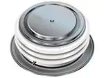
B-PUK (TO-200AC)
• Designed and qualified for industrial level
• Material categorization: for definitions of compliance
please see www.vishay.com/doc?99912
PRIMARY CHARACTERISTICS
Package
B-PUK (TO-200AC)
Circuit configuration
Single SCR
TYPICAL APPLICATIONS
• Inverters
IT(AV)
940 A
VDRM/VRRM
400 V, 800 V
VTM
1.63 V
ITSM at 50 Hz
20 000 A
• All types of force-commutated converters
ITSM at 60 Hz
20 950 A
IGT
200 mA
TC/Ths
55 °C
• Choppers
• Induction heating
MAJOR RATINGS AND CHARACTERISTICS
PARAMETER
TEST CONDITIONS
IT(AV)
Ths
IT(RMS)
Ths
ITSM
I2t
VALUES
UNITS
940
A
55
°C
1900
A
25
°C
50 Hz
20 000
60 Hz
20 950
50 Hz
2000
60 Hz
1820
VDRM/VRRM
400 to 800
tq
Range
TJ
A
kA2s
V
10 to 20
μs
-40 to +125
°C
IDRM/IRRM MAXIMUM
AT TJ = TJ MAXIMUM
mA
ELECTRICAL SPECIFICATIONS
VOLTAGE RATINGS
TYPE NUMBER
VS-ST733C..L
VOLTAGE
CODE
VDRM/VRRM, MAXIMUM
REPETITIVE PEAK VOLTAGE
V
VRSM, MAXIMUM
NON-REPETITIVE PEAK
VOLTAGE
V
04
400
500
08
800
900
75
Revision: 13-Sep-17
Document Number: 94378
1
For technical questions within your region: DiodesAmericas@vishay.com, DiodesAsia@vishay.com, DiodesEurope@vishay.com
THIS DOCUMENT IS SUBJECT TO CHANGE WITHOUT NOTICE. THE PRODUCTS DESCRIBED HEREIN AND THIS DOCUMENT
ARE SUBJECT TO SPECIFIC DISCLAIMERS, SET FORTH AT www.vishay.com/doc?91000
�VS-ST733CL Series
www.vishay.com
Vishay Semiconductors
CURRENT CARRYING CAPABILITY
ITM
FREQUENCY
ITM
ITM
180° el
UNITS
100 µs
180° el
50 Hz
2200
1900
3580
3100
6800
400 Hz
2050
1660
3600
3130
3750
3240
1000 Hz
1370
1070
2900
2450
2120
1780
2500 Hz
500
370
1220
980
960
Recovery voltage VR
Voltage before turn-on VD
50
50
VDRM
VDRM
VDRM
50
-
40
55
Equivalent values for RC circuit
V
-
40
10/0.47
A
770
50
Rise of on-state current dI/dt
Heatsink temperature
5920
55
10/0.47
A/μs
40
55
°C
/μF
10/0.47
ABSOLUTE MAXIMUM RATINGS
PARAMETER
SYMBOL
Maximum average on-state
current at heatsink temperature
IT(AV)
Maximum RMS on-state current
IT(RMS)
TEST CONDITIONS
180° conduction, half sine wave
double side (single side) cooled
DC at 25 °C heatsink temperature double side cooled
t = 10 ms
Maximum peak, one half cycle,
non-repetitive surge current
ITSM
t = 8.3 ms
t = 10 ms
t = 8.3 ms
t = 10 ms
Maximum I2t for fusing
I2t
t = 8.3 ms
t = 10 ms
t = 8.3 ms
Maximum
I2t
for fusing
Maximum peak on-state voltage
VALUES
A
55 (85)
°C
1900
No voltage
reapplied
20 000
100 % VRRM
reapplied
16 800
No voltage
reapplied
A
20 950
Sinusoidal half wave,
initial TJ = TJ maximum
100 % VRRM
reapplied
UNITS
940 (350)
17 600
2000
1820
kA2s
1410
1290
I2t
t = 0.1 ms to 10 ms, no voltage reapplied
VTM
ITM = 1700 A, TJ = TJ maximum,
tp = 10 ms sine wave pulse
1.63
kA2s
20 000
Low level value of threshold voltage
VT(TO)1
(16.7 % x x IT(AV) < I < x IT(AV)), TJ = TJ maximum
1.09
High level value of threshold voltage
VT(TO)2
V
(I > x IT(AV)), TJ = TJ maximum
1.20
Low level value of forward slope resistance
rt1
(16.7 % x x IT(AV) < I < x IT(AV)), TJ = TJ maximum
0.32
High level value of forward slope
resistance
rt2
(I > x IT(AV)), TJ = TJ maximum
0.29
Maximum holding current
IH
TJ = 25 °C, IT > 30 A
600
Typical latching current
IL
TJ = 25 °C, VA = 12 V, Ra = 6 , IG = 1 A
1000
m
mA
SWITCHING
PARAMETER
SYMBOL
Maximum non-repetitive rate of rise
of turned-on current
Typical delay time
Maximum turn-off time
minimum
maximum
dI/dt
TEST CONDITIONS
TJ = TJ maximum, VDRM = Rated VDRM, ITM = 2 x dI/dt
Gate pulse: 20 V 20 , 10 μs 0.5 μs rise time
td
TJ = 25 °C, VDM = Rated VDRM, ITM = 50 A DC, tp = 1 μs
Resistive load, gate pulse: 10 V, 5 source
tq
TJ = TJ maximum, ITM = 550 A, commutating dI/dt = 40 A/μs,
VR = 50 V, tp = 500 μs, dV/dt: see table in device code
VALUES
UNITS
1000
A/μs
1.5
10
μs
20
Revision: 13-Sep-17
Document Number: 94378
2
For technical questions within your region: DiodesAmericas@vishay.com, DiodesAsia@vishay.com, DiodesEurope@vishay.com
THIS DOCUMENT IS SUBJECT TO CHANGE WITHOUT NOTICE. THE PRODUCTS DESCRIBED HEREIN AND THIS DOCUMENT
ARE SUBJECT TO SPECIFIC DISCLAIMERS, SET FORTH AT www.vishay.com/doc?91000
�VS-ST733CL Series
www.vishay.com
Vishay Semiconductors
BLOCKING
PARAMETER
SYMBOL
TEST CONDITIONS
Maximum critical rate of rise of off-state voltage
dV/dt
TJ = TJ maximum, linear to 80 % VDRM,
higher value available on request
Maximum peak reverse and off-state leakage current
IRRM,
IDRM
TJ = TJ maximum, rated VDRM/VRRM applied
VALUES
UNITS
500
V/μs
75
mA
VALUES
UNITS
TRIGGERING
PARAMETER
SYMBOL
Maximum peak gate power
PGM
Maximum average gate power
PG(AV)
Maximum peak positive gate current
IGM
Maximum peak positive gate voltage
+VGM
Maximum peak negative gate voltage
-VGM
Maximum DC gate current required to trigger
IGT
Maximum DC gate voltage required to trigger
VGT
Maximum DC gate current not to trigger
IGD
Maximum DC gate voltage not to trigger
VGD
TEST CONDITIONS
60
TJ = TJ maximum, f = 50 Hz, d% = 50
10
10
TJ = TJ maximum, tp 5 ms
20
5
200
TJ = 25 °C, VA = 12 V, Ra = 6
TJ = TJ maximum, rated VDRM applied
W
A
V
mA
3
V
20
mA
0.25
V
VALUES
UNITS
THERMAL AND MECHANICAL SPECIFICATIONS
PARAMETER
SYMBOL
Maximum operating junction temperature range
Maximum storage temperature range
TEST CONDITIONS
TJ
-40 to +125
TStg
-40 to +150
Maximum thermal resistance, junction to heatsink
RthJ-hs
Maximum thermal resistance, case to heatsink
RthC-hs
DC operation single side cooled
0.073
DC operation double side cooled
0.031
DC operation single side cooled
0.011
DC operation double side cooled
K/W
0.005
Mounting force, ± 10 %
Approximate weight
Case style
°C
See dimensions - link at the end of datasheet
14 700
(1500)
N
(kg)
255
g
B-PUK (TO-200AC)
RthJ-hs CONDUCTION
CONDUCTION ANGLE
SINUSOIDAL CONDUCTION
RECTANGULAR CONDUCTION
SINGLE SIDE
DOUBLE SIDE
SINGLE SIDE
DOUBLE SIDE
180°
0.009
0.009
0.006
0.006
120°
0.011
0.011
0.011
0.011
90°
0.014
0.014
0.015
0.015
60°
0.020
0.021
0.021
0.022
30°
0.036
0.036
0.036
0.036
TEST CONDITIONS
UNITS
TJ = TJ maximum
K/W
Note
• The table above shows the increment of thermal resistance RthJ-hs when devices operate at different conduction angles than DC
Revision: 13-Sep-17
Document Number: 94378
3
For technical questions within your region: DiodesAmericas@vishay.com, DiodesAsia@vishay.com, DiodesEurope@vishay.com
THIS DOCUMENT IS SUBJECT TO CHANGE WITHOUT NOTICE. THE PRODUCTS DESCRIBED HEREIN AND THIS DOCUMENT
ARE SUBJECT TO SPECIFIC DISCLAIMERS, SET FORTH AT www.vishay.com/doc?91000
�VS-ST733CL Series
www.vishay.com
130
ST733C..L Series
(Single Side Cooled)
R thJ-hs (DC) = 0.073 K/W
120
110
Maximum Allowable Heatsink
Temperature (°C)
Maximum Allowable Heatsink
Temperature (°C)
130
Vishay Semiconductors
100
90
Conduction Angle
80
30°
70
60°
90°
60
120°
50
180°
40
ST733C..L Series
(Double Side Cooled)
R thJ-hs (DC) = 0.031 K/W
120
110
100
90
Conduction Period
80
70
30°
60
60°
50
90°
120°
40
180°
30
DC
20
0
100
200
300
400
500
600
0
700
Fig. 1 - Current Ratings Characteristics
100
90
Conduction Period
80
70
60
30°
50
60°
90°
40
120°
30
180°
DC
20
0
200
400
600
800
180°
120°
90°
60°
30°
2000
1000
Conduction Angle
500
ST733C..L Series
TJ = 125°C
0
1000
0
110
100
90
Conduction Angle
80
70
60
30°
50
60°
40
90°
30
120°
180°
400
600
800
1000 1200 1400
Fig. 5 - On-State Power Loss Characteristics
2500
Maximum Average On-state
Power Loss (W)
Maximum Allowable Heatsink
Temperature (°C)
ST733C..L Series
(Double Side Cooled)
R thJ-hs (DC) = 0.031 K/W
200
Average On-state Current (A)
Fig. 2 - Current Ratings Characteristics
120
RMS Limit
1500
Average On-state Current (A)
130
2000
2500
Maximum Average On-state
Power Loss (W)
Maximum Allowable Heatsink
Temperature (°C)
110
1500
Fig. 4 - Current Ratings Characteristics
ST733C..L Series
(Single Side Cooled)
R thJ-hs (DC) = 0.073 K/W
120
1000
Average On-state Current (A)
Average On-state Current (A)
130
500
180°
120°
90°
60°
30°
2000
RMS Limit
1500
1000
Conduction Angle
500
ST733C..L Series
TJ = 125°C
0
20
0
200
400
600
800
1000 1200 1400
Average On-state Current (A)
Fig. 3 - Current Ratings Characteristics
0
200
400
600
800
1000
1200
1400
Average On-state Current (A)
Fig. 6 - On-State Power Loss Characteristics
Revision: 13-Sep-17
Document Number: 94378
4
For technical questions within your region: DiodesAmericas@vishay.com, DiodesAsia@vishay.com, DiodesEurope@vishay.com
THIS DOCUMENT IS SUBJECT TO CHANGE WITHOUT NOTICE. THE PRODUCTS DESCRIBED HEREIN AND THIS DOCUMENT
ARE SUBJECT TO SPECIFIC DISCLAIMERS, SET FORTH AT www.vishay.com/doc?91000
�VS-ST733CL Series
www.vishay.com
At Any Rated Load Condition And With
Rated VRRM Applied Following Surge.
Initial TJ = 125°C
at 60 Hz 0.0083 s
at 50 Hz 0.0100 s
16 000
14 000
12 000
10 000
ST733C..L Series
8000
1
10
100
Number Of Equal Amplitude
Half Cycle Current Pulses (N)
ZthJ-hs - Transient Thermal Impedance (K/W)
Peak Half Sine Wave
On-state Current (A)
18 000
Vishay Semiconductors
18 000
16 000
14 000
12 000
10 000
ST733C..L Series
8000
0.01
0.1
1
Pulse Train Duration (s)
Qrr - Maximum Reverse Recovery Charge (μC)
Peak Half Sine Wave
On-state Current (A)
Maximum Non Repetitive Surge Current
Versus Pulse Train Duration. Control
Of Conduction May Not Be Maintained.
Initial TJ = 125°C
No Voltage Reapplied
Rated VRRM Reapplied
TJ = 25 °C
1000
TJ = 125 °C
ST733C..L Series
100
0.5
1
1.5
2
2.5
3
3.5
4
4.5
Instantaneous On-state Voltage (V)
Fig. 9 - On-State Voltage Drop Characteristics
0.01
Steady State Value
R thJ-hs = 0.073 K/W
(Single Side Cooled)
R thJ-hs = 0.031 K/W
(Double Side Cooled)
(DC Operation)
0.001
0.001
0.01
0.1
1
10
100
Square Wave Pulse Duration (s)
450
I TM = 1500 A
ST733C..L Series
TJ = 125 °C
400
350
300
1000 A
250
500 A
200
150
100
50
0
10
20
30
40
50
60
70
80
90
100
dIFdt - Rate of Fall of On-State Current (A/μs)
Fig. 11 - Reverse Recovered Charge Characteristics
Irr - Maximum Reverse Recovery Current (A)
Instantaneous On-state Current (A)
Fig. 8 - Maximum Non-Repetitive Surge Current
Single and Double Side Cooled
10 000
ST733C..L Series
Fig. 10 - Thermal Impedance ZthJC Characteristics
Fig. 7 - Maximum Non-Repetitive Surge Current
Single and Double Side Cooled
20 000
0.1
250
I TM= 1500 A
200
1000 A
150
500 A
100
ST733C..L Series
TJ = 125 °C
50
0
10
20
30
40
50
60
70
80
90
100
dIFdt - Rate of Fall of Forward Current (A/μs)
Fig. 12 - Reverse Recovered Current Characteristics
Revision: 13-Sep-17
Document Number: 94378
5
For technical questions within your region: DiodesAmericas@vishay.com, DiodesAsia@vishay.com, DiodesEurope@vishay.com
THIS DOCUMENT IS SUBJECT TO CHANGE WITHOUT NOTICE. THE PRODUCTS DESCRIBED HEREIN AND THIS DOCUMENT
ARE SUBJECT TO SPECIFIC DISCLAIMERS, SET FORTH AT www.vishay.com/doc?91000
�VS-ST733CL Series
www.vishay.com
Vishay Semiconductors
Snubber circuit
RS = 10 Ω
CS = 0.47 μF
VD = 80 % VDRM
1E4
50 Hz
400 200100
1000
1500
2500
3000
1E3
5000
tp
ST733C..L Series
Sinusoidal pulse
TC = 40°C
1E5
Peak On-state Current (A)
Peak On-state Current (A)
1E5
1E2
1E3
1E4
400 200 100 50 Hz
1000
1500
2500
1E3
3000
5000
1E2
1E1
Snubber circuit
RS = 10 Ω
CS = 0.47 μF
VD = 80 % VDRM
tp
ST733C..L Series
Sinusoidal pulse
TC = 55 °C
1E2
1E4
1E1
Pulse Basewidth (μs)
1E2
1E3
1E4
Pulse Basewidth (μs)
Fig. 13 - Frequency Characteristics
1E5
Snubber circuit
RS = 10 Ω
CS = 0.47 μF
VD = 80 % VDRM
tp
ST733C..L Series
Trapezoidal pulse
TC = 40°C
di/dt = 50A/μs
1E4
50 Hz
100
400
200
500
1000
1500
2000
2500
3000
1E3
Peak On-state Current (A)
Peak On-state Current (A)
1E5
Snubber circuit
RS = 10 Ω
CS = 0.47 μF
VD = 80 % VDRM
1E4
1000
1500
1E3
500 400
50 Hz
200100
2000
2500
3000
5000
1E2
tp
ST733C..L Series
Trapezoidal pulse
TC = 55 °C
di/dt = 50 A/μs
1E2
1E1
1E2
1E3
1E1
1E4
Pulse Basewidth (μs)
1E2
1E3
1E4
Pulse Basewidth (μs)
Fig. 14 - Frequency Characteristics
1E5
Snubber circuit
RS = 10 Ω
CS = 0.47 μF
VD = 80 % VDRM
tp
ST733C..L Series
Trapezoidal pulse
TC = 40°C
di/dt = 50A/μs
1E4
500
1000
1500
2000
2500
3000
5000
1E3
400 200
100
50 Hz
1E2
Peak On-state Current (A)
Peak On-state Current (A)
1E5
Snubber circuit
RS = 10 Ω
CS = 0.47 μF
VD = 80 % VDRM
ST733C..L Series
Trapezoidal pulse
T = 55 °C
di/dt = 50A/μs
tp
1E4
500
400 200
100 50 Hz
1000
1500
2000
2500
3000
1E3
1E2
1E1
1E2
1E3
1E4
1E1
1E2
1E3
1E4
Pulse Basewidth (μs)
Pulse Basewidth (μs)
Fig. 15 - Frequency Characteristics
Revision: 13-Sep-17
Document Number: 94378
6
For technical questions within your region: DiodesAmericas@vishay.com, DiodesAsia@vishay.com, DiodesEurope@vishay.com
THIS DOCUMENT IS SUBJECT TO CHANGE WITHOUT NOTICE. THE PRODUCTS DESCRIBED HEREIN AND THIS DOCUMENT
ARE SUBJECT TO SPECIFIC DISCLAIMERS, SET FORTH AT www.vishay.com/doc?91000
�VS-ST733CL Series
www.vishay.com
Vishay Semiconductors
1E5
tp
ST733C..L Series
Sinusoidal pulse
1E4
2
3
5
Peak On-state Current (A)
Peak On-state Current (A)
1E5
20 joules per pulse
10
1
1E3
0.5
0.4
0.3
1E2
tp
1E4
1E2
1E3
20 joules per pulse
10
5
3
1E3
2
1
0.5
1E2
0.4
0.3
1E1
1E1
ST733C..L Series
Rectangular pulse
di/dt = 50 A/μs
1E1
1E4
1E1
Pulse Basewidth (μs)
1E2
1E3
1E4
Pulse Basewidth (μs)
Fig. 16 - Maximum On-State Energy Power Loss Characteristics
(1) PGM = 10 W, tp = 20 ms
(2) PGM = 20 W, tp = 10 ms
(3) PGM = 40 W, tp = 5 ms
(4) PGM = 60 W, tp = 3.3 ms
Rectangular gate pulse
a) Recommended load line for
rated di/dt : 20 V, 10 Ω; tr