VS-T40HFL, VS-T70HFL, VS-T85HFL Series
www.vishay.com
Vishay Semiconductors
Fast Recovery Diodes (T-Modules), 40 A, 70 A, 85 A
FEATURES
• Fast recovery time characteristics
• Electrically isolated base plate
• 3500 VRMS isolating voltage
• Standard JEDEC® package
• Simplified mechanical designs, rapid assembly
• Large creepage distances
• UL E78996 approved
• Designed and qualified for industrial level
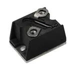
D-55 (T-module)
• Material categorization: for definitions of compliance
please see www.vishay.com/doc?99912
DESCRIPTION
The series of T-modules uses fast recovery power diodes in
a single diode configuration. The semiconductors are
electrically isolated from the metal base, allowing common
heatsink and compact assemblies to be built.
These single diode modules can be used in conjunction with
the thyristor modules as a freewheel diode. Application
includes self-commutated inverters, DC choppers, motor
control, inductive heating and electronic welders. These
modules are intended for those applications where very fast
recovery characteristics are required and for general power
switching applications.
PRIMARY CHARACTERISTICS
IF(AV)
40 A, 70 A, 85 A
Type
Modules - diode, fast
VRRM
100 V to 1000 V
Package
D-55 (T-module)
Circuit configuration
Single
MAJOR RATINGS AND CHARACTERISTICS
SYMBOL
IF(AV)
CHARACTERISTICS
I2t
T70HFL
T85HFL
UNITS
40
70
85
A
TC
70
70
70
°C
63
110
133
A
50 Hz
475
830
1300
60 Hz
500
870
1370
50 Hz
1130
3460
8550
60 Hz
1030
3160
7810
IF(RMS)
IFSM
VALUES
T40HFL
A
A2s
VRRM
Range
100 to 1000
V
trr
Range
200 to 1000
ns
TJ
Range
-40 to +125
°C
ELECTRICAL SPECIFICATIONS
VOLTAGE RATINGS
TYPE
NUMBER
VS_T40HFL..
VS_T70HFL..
VS_T85HFL..
VRRM, MAXIMUM REPETITIVE VRSM, MAXIMUM NON-REPETITIVE
PEAK REVERSE VOLTAGE
PEAK REVERSE VOLTAGE
V
V
VOLTAGE
CODE
trr
CODE
10
S02, S05, S10
100
150
20
S02, S05, S10
200
300
40
S02, S05, S10
400
500
60
S02, S05, S10
600
700
80
S05, S10
800
900
100
S05, S10
1000
1100
IRRM MAXIMUM
AT TJ = 25 °C
μA
100
Revision: 24-Sep-2021
Document Number: 93184
1
For technical questions within your region: DiodesAmericas@vishay.com, DiodesAsia@vishay.com, DiodesEurope@vishay.com
THIS DOCUMENT IS SUBJECT TO CHANGE WITHOUT NOTICE. THE PRODUCTS DESCRIBED HEREIN AND THIS DOCUMENT
ARE SUBJECT TO SPECIFIC DISCLAIMERS, SET FORTH AT www.vishay.com/doc?91000
�VS-T40HFL, VS-T70HFL, VS-T85HFL Series
www.vishay.com
Vishay Semiconductors
FORWARD CONDUCTION
PARAMETER
SYMBOL
Maximum average forward current
at case temperature
Maximum RMS forward current
40
t = 8.3 ms
IFSM
t = 10 ms
t = 8.3 ms
t = 10 ms
t = 8.3 ms
Maximum I2t for fusing
I2t
t = 10 ms
t = 8.3 ms
I2√t
for fusing
70
85
70
IF(RMS)
Maximum peak, one-cycle forward,
non-repetitive surge current
Maximum
T40HFL T70HFL T85HFL
180° conduction, half sine wave
IF(AV)
t = 10 ms
I2√t
VALUES
TEST CONDITIONS
63
110
133
No voltage
reapplied
830
1300
500
870
1370
100 %
VRRM
reapplied
400
700
1100
420
730
1150
1130
3460
8550
1030
3160
7810
800
2450
6050
730
2230
5520
11 300
34 600
85 500
No voltage
reapplied
100 %
VRRM
reapplied
t = 0.1 ms to 10 ms, no voltage reapplied
A
°C
475
Sinusoidal half wave,
initial TJ = TJ maximum
UNITS
Low level value of threshold voltage
VF(TO)1
TJ = 25 °C, (16.7 % x π x IF(AV) < I < π x IF(AV))
0.82
0.87
0.84
High level value of threshold
voltage
VF(TO)2
TJ = 25 °C, (I > π x IF(AV))
0.84
0.90
0.86
Low level value of forward slope
resistance
rf1
TJ = 25 °C, (16.7 % x π x IF(AV) < I < π x IF(AV))
7.0
2.77
2.15
High level value of forward
slope resistance
rf2
TJ = 25 °C, (I > π x IF(AV))
6.8
2.67
2.07
IFM = π x IF(AV), TJ = 25 °C, tp = 400 μs square wave
Average power = VF(TO) x IF(AV) + rf x (IF(RMS))2
1.60
1.73
1.55
A
A
A2s
A2√s
V
mΩ
Maximum forward voltage drop
VFM
V
REVERSE RECOVERY CHARACTERISTICS
PARAMETER
SYMBOL
Maximum reverse
recovery time
trr
Maximum reverse
recovery charge
Qrr
T40HFL
TEST CONDITIONS (1)
T70HFL
T85HFL
S02
S05
S10
S02
S05
S10
S02
S05
S10
TJ = 25 °C, -dIF/dt = 100 A/μs
IF = 1 A to VR = 30 V
70
110
270
70
110
270
80
120
290
TJ = 25 °C, -dIF/dt = 25 A/μs
IFM = π x rated IF(AV), VR = - 30 V
200
500
1000
200
500
1000
200
500
1000
TJ = 25 °C, -dIF/dt = 100 A/μs
IF = 1 A to VR = 30 V
0.25
0.4
1.35
0.25
0.4
1.35
0.3
0.6
1.6
TJ = 25 °C, -dIF/dt = 25 A/μs
IFM = π x rated IF(AV), VR = - 30 V
0.55
2.0
8.0
0.6
2.1
8.5
0.8
3.5
1.5
UNITS
ns
μC
Note
(1) Tested on LEM 300 A diodemeter tester
BLOCKING
PARAMETER
Maximum peak reverse leakage current
RMS isolation voltage
SYMBOL
TEST CONDITIONS
IRRM
TJ = 125 °C
VISOL
50 Hz, circuit to base, all terminals shorted,
TJ = 25 °C, t = 1 s
T40HFL T70HFL T85HFL UNITS
20
mA
3500
V
Revision: 24-Sep-2021
Document Number: 93184
2
For technical questions within your region: DiodesAmericas@vishay.com, DiodesAsia@vishay.com, DiodesEurope@vishay.com
THIS DOCUMENT IS SUBJECT TO CHANGE WITHOUT NOTICE. THE PRODUCTS DESCRIBED HEREIN AND THIS DOCUMENT
ARE SUBJECT TO SPECIFIC DISCLAIMERS, SET FORTH AT www.vishay.com/doc?91000
�VS-T40HFL, VS-T70HFL, VS-T85HFL Series
www.vishay.com
Vishay Semiconductors
THERMAL AND MECHANICAL SPECIFICATIONS
PARAMETER
SYMBOL
Junction operating temperature range
Storage temperature range
Maximum internal thermal
resistance, junction to case
per module
VALUES
-40 to +125
TStg
-40 to +150
T40HFL
UNITS
°C
0.85
RthJC
T70HFL
DC operation
0.53
T85HFL
K/W
0.46
Thermal resistance,
case to heatsink per module
Mounting surface, flat,
smooth and greased
RthCS
base to heatsink
Mounting torque ± 10 %
TEST CONDITIONS
TJ
M3.5 mounting screws (1)
Non-lubricated
threads
busbar to terminal
0.2
1.3 ± 10 %
M5 screws terminals
3 ± 10 %
See dimensions link at the end of datasheet
Approximate weight
Case style
Nm
54
g
19
oz.
D-55 (T-module)
Note
(1) A mounting compound is recommended and the torque should be rechecked after a period of about 3 hours to allow for the spread of
the compound
ΔR CONDUCTION
SINUSOIDAL CONDUCTION AT TJ MAXIMUM
DEVICES
RECTANGULAR CONDUCTION AT TJ MAXIMUM
180°
120°
90°
60°
30°
180°
120°
90°
60°
30°
T40HFL
0.06
0.08
0.10
0.14
0.24
0.05
0.08
0.10
0.15
0.24
T70HFL
0.05
0.06
0.08
0.11
0.19
0.04
0.06
0.08
0.12
0.19
T85HFL
0.04
0.05
0.06
0.09
0.15
0.03
0.05
0.07
0.09
0.015
UNITS
K/W
130
T40HFL.. Series
R thJC (DC) = 0.85 K/ W
120
110
100
Conduc tion Angle
90
80
30°
70
60°
90°
60
120°
180°
50
0
10
20
30
40
50
Maximum Allowa ble Case Temperature (°C)
Maximum Allowab le Case Temperature (°C)
Note
• The table above shows the increment of thermal resistance RthJC when devices operate at different conduction angles than DC
130
T40HFL.. Series
R thJC (DC) = 0.85 K/ W
120
110
100
Conduc tion Period
90
80
30°
60°
70
90°
120°
180°
60
DC
50
0
10
20
30
40
50
60
70
Average Forward Current (A)
Average Forward Current (A)
Fig. 1 - Current Ratings Characteristics
Fig. 2 - Current Ratings Characteristics
Revision: 24-Sep-2021
Document Number: 93184
3
For technical questions within your region: DiodesAmericas@vishay.com, DiodesAsia@vishay.com, DiodesEurope@vishay.com
THIS DOCUMENT IS SUBJECT TO CHANGE WITHOUT NOTICE. THE PRODUCTS DESCRIBED HEREIN AND THIS DOCUMENT
ARE SUBJECT TO SPECIFIC DISCLAIMERS, SET FORTH AT www.vishay.com/doc?91000
�VS-T40HFL, VS-T70HFL, VS-T85HFL Series
T70HFL.. Series
R thJC (DC) = 0.53 K/ W
120
110
100
Conduction Angle
90
80
30°
70
60°
90°
120°
60
180°
50
0
10
20
30
40
50
60
70
80
Maximum Allowable Case Temperature (°C)
130
Vishay Semiconductors
130
T85HFL.. Series
R thJC (DC) = 0.46 K/ W
120
110
100
Conduction Period
90
80
30°
70
60°
90°
120°
60
180°
DC
50
0
20
40
60
80
100
120
140
Average Forward Current (A)
Fig. 3 - Current Ratings Characteristics
Fig. 6 - Current Ratings Characteristics
130
T70HFL.. Series
RthJC (DC) = 0.53 K/ W
120
110
100
Conduction Period
90
80
30°
70
60°
90°
120°
60
180°
DC
50
0
20
40
60
80
100
120
Maximum Average Forward Power Lo ss (W)
Average Forward Current (A)
70
180°
120°
90°
60°
30°
60
50
RMSLimit
40
30
20
Conduc tion Angle
10
T40HFL.. Series
TJ= 125°C
0
0
5
10
15
20
25
30
35
40
Average Forward Current (A)
Average Forward Current (A)
Fig. 4 - Current Ratings Characteristics
Fig. 7 - Forward Power Loss Characteristics
130
T85HFL.. Series
R thJC (DC) = 0.46 K/ W
120
110
100
Conduc tion Angle
90
80
30°
70
60°
90°
120°
60
180°
50
0
10
20
30
40
50
60
70
80
90
Ma ximum Average Forward Power Lo ss (W)
Maximum Allowable Case Temperature (°C)
Maximum Allowa ble Case Temperature (°C)
Maximum Allowable Case Temp erature (°C)
www.vishay.com
90
DC
180°
120°
90°
60°
30°
80
70
60
50
RMS Limit
40
30
Conduc tion Period
20
T40HFL.. Series
T J = 125°C
10
0
0
10
20
30
40
50
60
70
Average Forward Current (A)
Average Forward Current (A)
Fig. 5 - Current Ratings Characteristics
Fig. 8 - Forward Power Loss Characteristics
Revision: 24-Sep-2021
Document Number: 93184
4
For technical questions within your region: DiodesAmericas@vishay.com, DiodesAsia@vishay.com, DiodesEurope@vishay.com
THIS DOCUMENT IS SUBJECT TO CHANGE WITHOUT NOTICE. THE PRODUCTS DESCRIBED HEREIN AND THIS DOCUMENT
ARE SUBJECT TO SPECIFIC DISCLAIMERS, SET FORTH AT www.vishay.com/doc?91000
�VS-T40HFL, VS-T70HFL, VS-T85HFL Series
180°
120°
90°
60°
30°
90
80
70
60
RMS Limit
50
40
30
Conduc tion Angle
20
T70HFL.. Series
TJ= 125°C
10
0
Maximum Average Forward Power Loss (W)
0
10
20
30
40
50
60
Maximum Average Forward Power Loss (W)
100
Vishay Semiconductors
160
120
100
80
RMSLimit
60
Conduc tion Period
40
T85HFL.. Series
TJ = 125°C
20
0
0
70
20
40
60
80
100
120
140
Average Forward Current (A)
Average Forward Current (A)
Fig. 9 - Forward Power Loss Characteristics
Fig. 12 - Forward Power Loss Characteristics
140
DC
180°
120°
90°
60°
30°
120
100
80
RMS Limit
60
Conduc tion Period
40
T70HFL.. Series
TJ = 125°C
20
0
0
20
40
60
80
100
180°
120°
90°
60°
30°
80
70
RMS Limit
60
50
40
Conduc tion Angle
30
T85HFL.. Series
TJ= 125°C
20
10
0
0
10
20
30
40
50
60
70
80
400
350
300
250
200
150
T40HFL.. Series
100
1
10
100
Fig. 13 - Maximum Non-Repetitive Surge Current
Peak Half Sine Wave Forwa rd Current (A)
110
90
At Any Ra ted Loa d Cond ition And With
Rated V RRM App lied Following Surge.
Initial T J= 125°C
@ 60 Hz 0.0083 s
@ 50 Hz 0.0100 s
Number Of Equal Amplitude Half Cycle Current Pulses (N)
Fig. 10 - Forward Power Loss Characteristics
100
450
120
Average Forward Current (A)
Maximum Average Forward Power Loss (W)
DC
180°
120°
90°
60°
30°
140
Peak Half Sine Wave Forwa rd Current (A)
Maximum Average Forward Power Loss (W)
www.vishay.com
90
Average Forward Current (A)
Fig. 11 - Forward Power Loss Characteristics
500
450
400
Maximum Non Repetitive Surge Current
Versus Pulse Train Duration.
Initial TJ = 125°C
No Voltage Reapplied
Rated VRRM Reapplied
350
300
250
200
150
100
0.01
T40HFL.. Series
0.1
1
Pulse Train Duration (s)
Fig. 14 - Maximum Non-Repetitive Surge Current
Revision: 24-Sep-2021
Document Number: 93184
5
For technical questions within your region: DiodesAmericas@vishay.com, DiodesAsia@vishay.com, DiodesEurope@vishay.com
THIS DOCUMENT IS SUBJECT TO CHANGE WITHOUT NOTICE. THE PRODUCTS DESCRIBED HEREIN AND THIS DOCUMENT
ARE SUBJECT TO SPECIFIC DISCLAIMERS, SET FORTH AT www.vishay.com/doc?91000
�VS-T40HFL, VS-T70HFL, VS-T85HFL Series
Vishay Semiconductors
800
At Any Ra ted Loa d Cond ition And With
Rated V RRM App lied Following Surge.
Initial TJ = 125°C
@ 60 Hz 0.0083 s
@ 50 Hz 0.0100 s
700
600
500
400
300
T70HFL.. Series
200
1
10
100
Peak Half Sine Wave Forward Current (A)
Peak Half Sine Wave Forward Current (A)
www.vishay.com
1300
Ma ximum Non Rep etitive Surge Current
Versus Pulse Train Dura tion.
Initial TJ = 125°C
No Voltage Reapplied
Rated V RRM Reapplied
1200
1100
1000
900
800
700
600
500
T85HFL.. Series
400
300
0.01
0.1
Number Of Equal Amplitude Half Cycle Current Pulses (N)
Maximum Non Repetitive Surge Current
Versus Pulse Train Duration.
Initial T J= 125°C
No Voltage Reapplied
Rated V RRM Reapplied
750
650
550
450
350
250
T70HFL.. Series
150
0.01
0.1
1
Pulse Train Duration (s)
Peak Half Sine Wave Forward Current (A)
At Any Rated Load Condition And With
Rated V RRM Ap p lied Following Surge.
Initial T J= 125°C
@ 60 Hz 0.0083 s
@ 50 Hz 0.0100 s
1100
1000
900
800
700
600
500
T85HFL.. Series
400
300
1
10
0.5
I FM= 300A
0.49
220A
172A
0.48
100A
50A
0.47
0.46
T40HFL..S02
T70HFL..S02
TJ = 125 °C
0.45
10
100
Ra te Of Fa ll Of Forwa rd Current - di/ d t (A/ µs)
Fig. 16 - Maximum Non-Repetitive Surge Current
1200
0.51
100
Number Of Equal Amplitude Half Cycle Current Pulses (N)
Fig. 17 - Maximum Non-Repetitive Surge Current
Fig. 19 - Recovery Time Characteristics
Maximum Reverse Rec overy Charge - Qrr (µC)
Peak Half Sine Wave Forward Current (A)
850
Fig. 18 - Maximum Non-Repetitive Surge Current
Maximum Reverse Rec overy Time - Trr (µs)
Fig. 15 - Maximum Non-Repetitive Surge Current
1
Pulse Train Duration (s)
8
7
6
I FM= 300A
220A
172A
100A
50A
5
4
3
2
T40HFL..S02
T70HFL..S02
TJ = 125 °C
1
10 20 30 40 50 60 70 80 90 100
Ra te Of Fa ll Of Forward Current - d i/ d t (A/ µs)
Fig. 20 - Recovery Charge Characteristics
Revision: 24-Sep-2021
Document Number: 93184
6
For technical questions within your region: DiodesAmericas@vishay.com, DiodesAsia@vishay.com, DiodesEurope@vishay.com
THIS DOCUMENT IS SUBJECT TO CHANGE WITHOUT NOTICE. THE PRODUCTS DESCRIBED HEREIN AND THIS DOCUMENT
ARE SUBJECT TO SPECIFIC DISCLAIMERS, SET FORTH AT www.vishay.com/doc?91000
�VS-T40HFL, VS-T70HFL, VS-T85HFL Series
Vishay Semiconductors
20
18
16
I FM= 300A
220A
172A
100A
50A
14
12
10
8
T40HFL..S02
T70HFL..S02
TJ = 125 °C
6
4
10 20 30 40 50 60 70 80 90 100
Ra te Of Fa ll Of Forward Current - d i/ d t (A/ µs)
1.1
1
I FM= 300A
0.9
220A
172A
100A
0.8
50A
0.7
T40HFL..S05
T70HFL..S05
TJ = 125 °C
0.6
10
28
26
I FM= 300A
220A
172A
100A
50A
24
22
20
18
16
14
12
T40HFL..S05
T70HFL..S05
TJ = 125 °C
10
8
6
10 20 30 40 50 60 70 80 90 100
Ra te Of Fa ll Of Forward Current - d i/ d t (A/ µs)
Fig. 24 - Recovery Current Characteristics
Maximum Reverse Rec overy Time - Trr (µs)
Maximum Reverse Rec overy Time - Trr (µs)
Fig. 21 - Recovery Current Characteristics
Maximum Reverse Rec overy Current - Irr (A)
Maximum Re verse Rec overy Current - Irr (A)
www.vishay.com
100
1.8
1.7
I FM= 300A
1.6
200A
1.5
100A
1.4
50A
1.3
1.2
1.1
T40HFL..S10
T70HFL..S10
TJ = 125 °C
1
10
100
Fig. 22 - Recovery Time Characteristics
Fig. 25 - Recovery Time Characteristics
20
18
16
I FM= 300A
220A
172A
100A
50A
14
12
10
8
6
T40HFL..S05
T70HFL..S05
TJ = 125 °C
4
10 20 30 40 50 60 70 80 90 100
Ra te Of Fa ll Of Forward Current - di/ d t (A/ µs)
Fig. 23 - Recovery Charge Characteristics
Maximum Reverse Re covery Charge - Qrr (µC)
Ra te Of Fa ll Of Forwa rd Current - d i/ d t (A/ µs)
Maximum Reverse Recovery Charge - Qrr (µC)
Ra te Of Fa ll Of Fo rwa rd Current - di/ dt (A/ µs)
40
35
I FM= 300A
200A
30
100A
25
50A
20
15
10
T40HFL..S10
T70HFL..S10
TJ = 125 °C
5
10 20 30 40 50 60 70 80 90 100
Ra te Of Fa ll Of Forward Current - d i/ d t (A/ µs)
Fig. 26 - Recovery Charge Characteristics
Revision: 24-Sep-2021
Document Number: 93184
7
For technical questions within your region: DiodesAmericas@vishay.com, DiodesAsia@vishay.com, DiodesEurope@vishay.com
THIS DOCUMENT IS SUBJECT TO CHANGE WITHOUT NOTICE. THE PRODUCTS DESCRIBED HEREIN AND THIS DOCUMENT
ARE SUBJECT TO SPECIFIC DISCLAIMERS, SET FORTH AT www.vishay.com/doc?91000
�VS-T40HFL, VS-T70HFL, VS-T85HFL Series
45
Vishay Semiconductors
I FM= 300A
200A
40
100A
35
50A
30
25
20
T40HFL..S10
T70HFL..S10
TJ = 125 °C
15
10
10 20 30 40 50 60 70 80 90 100
Maximum Reverse Rec overy Current - Irr (A)
Maximum Reverse Rec overy Current - Irr (A)
www.vishay.com
28
26
24
IFM = 300A
200A
100A
50A
22
20
18
16
14
12
10
8
T85HFL..S02
TJ = 125°C
6
10 20 30 40 50 60 70 80 90 100
Ra te Of Fall Of Forwa rd Current - di/ d t (A/ µs)
Fig. 27 - Recovery Current Characteristics
Fig. 30 - Recovery Current Characteristics
Maximum Reverse Rec overy Time - Trr (µs)
1.2
1.1
1
IFM = 300A
0.9
200A
100A
0.8
50A
0.7
T85HFL..S02
T J = 125°C
0.6
10
100
Ra te Of Fa ll Of Forwa rd Current - di/ dt (A/ µs)
Maximum Reverse Rec overy Charge - Qrr (µC)
Fig. 28 - Recovery Time Characteristics
25
IFM = 300A
20
200A
100A
15
50A
10
T85HFL..S02
TJ = 125 °C
5
10 20 30 40 50 60 70 80 90 100
Rate Of Fall Of Forward Current - di/ dt (A/ µs)
Fig. 29 - Recovery Charge Characteristics
1.3
1.2
IFM = 300A
1.1
200A
1
100A
50A
0.9
T85HFL..S05
TJ = 125°C
0.8
10
100
Ra te Of Fall Of Forward Current - di/ d t (A/ µs)
Fig. 31 - Recovery Time Characteristics
Maximum Reverse Recovery Charge - Qrr (µC)
Maximum Reverse Recovery Time - Trr (µs)
Ra te Of Fa ll Of Forwa rd Current - di/ d t (A/ µs)
30
IFM = 300A
27
200A
24
21
18
100A
50A
15
12
9
T85HFL..S05
TJ = 125°C
6
10 20 30 40 50 60 70 80 90 100
Ra te Of Fall Of Forwa rd Current - di/ d t (A/ µs)
Fig. 32 - Recovery Charge Characteristics
Revision: 24-Sep-2021
Document Number: 93184
8
For technical questions within your region: DiodesAmericas@vishay.com, DiodesAsia@vishay.com, DiodesEurope@vishay.com
THIS DOCUMENT IS SUBJECT TO CHANGE WITHOUT NOTICE. THE PRODUCTS DESCRIBED HEREIN AND THIS DOCUMENT
ARE SUBJECT TO SPECIFIC DISCLAIMERS, SET FORTH AT www.vishay.com/doc?91000
�VS-T40HFL, VS-T70HFL, VS-T85HFL Series
www.vishay.com
Vishay Semiconductors
Maximum Reverse Rec overy Charge - Qrr (µC)
Maximum Reverse Rec overy Current - Irr (A)
35
IFM = 300A
200A
30
100A
50A
25
20
15
T85HFL..S05
TJ = 125°C
10
10 20 30 40 50 60 70 80 90 100
Ra te Of Fall Of Forwa rd Current - di/ dt (A/ µs)
Maximum Reverse Rec overy Current - Irr (A)
Maximum Reverse Rec overy Time - Trr (µs)
1.9
1.8
IFM = 300A
200A
1.5
100A
1.4
1.3
1.2
50A
T85HFL..S10
TJ = 125°C
1.1
1
10
45
200A
40
100A
35
30
50A
25
20
T85HFL..S10
TJ = 125°C
15
10
10 20 30 40 50 60 70 80 90 100
Fig. 35 - Recovery Charge Characteristics
2
1.6
IFM = 300A
50
Ra te Of Fa ll Of Forwa rd Current - di/ d t (A/ µs)
Fig. 33 - Recovery Current Characteristics
1.7
55
100
60
IFM = 300A
55
200A
50
100A
45
50A
40
35
30
25
T85HFL..S10
TJ = 125°C
20
15
10 20 30 40 50 60 70 80 90 100
Rate Of Fall Of Forwa rd Current - d i/ dt (A/µs)
Ra te Of Fa ll Of Forward Current - di/ dt (A/ µs)
Fig. 36 - Recovery Current Characteristics
Fig. 34 - Recovery Time Characteristics
Peak Forward Current (A)
1E4
tp
T40HFL.. Series
Trapezoidal Pulse
T C = 70 °C
1E3
1E2
20000 10000
5000 2500 1500 1000
400
200
50 Hz
5000 2500 1500 1000
tp
1E1
1E1
400
200
50 Hz
T40HFL.. Series
Sinusoidal Pulse
T = 70°C
C
1E2
1E3
1E1
1E4 1E1
1E4
1E2
Pulse Basewidth (µs)
1E3
1E4
Pulse Basewidth (µs)
Fig. 37 - Frequency Characteristics
Revision: 24-Sep-2021
Document Number: 93184
9
For technical questions within your region: DiodesAmericas@vishay.com, DiodesAsia@vishay.com, DiodesEurope@vishay.com
THIS DOCUMENT IS SUBJECT TO CHANGE WITHOUT NOTICE. THE PRODUCTS DESCRIBED HEREIN AND THIS DOCUMENT
ARE SUBJECT TO SPECIFIC DISCLAIMERS, SET FORTH AT www.vishay.com/doc?91000
�VS-T40HFL, VS-T70HFL, VS-T85HFL Series
www.vishay.com
Vishay Semiconductors
1E4
Peak Forward Current (A)
tp
T40HFL..
Trapezoidal Pulse
TC= 90 °C
1E3
1E2
20000 10000 5000 2500 1500 1000
400
200
50 Hz
5000
tp
1E1
1E1
2500 1500 1000
400
200
50 Hz
T40HFL.. Series
Sinusoidal Pulse
TC= 90°C
1E2
1E1
1E1E4
4 E1
1E3
1E2
Pulse Basewidth (µs)
1E3
1E4
Pulse Basewidth (µs)
Fig. 38 - Frequency Characteristics
1E4
Peak Forward Current (A)
20 joules per pulse
1E3
0.1
0.04
0.02
1E2
0.2
0.4
1
2
4
10
0.4
0.04
0.02
0.01
0.01
1E1
tp
1E0
1E1
T40HFL.. Series
Sinusoid al Pulse
TJ = 125 °C
1E2
tp
1E3
1E1E4
4 1E1
1E1
1
2
10
4
20 joules per pulse
0.2
0.1
T40HFL.. Series
Trapezoidal Pulse
TJ= 125°C
di/ dt = 50A/ µs
1E2
Pulse Basewidth (µs)
1E3
1E4
Pulse Basewidth (µs)
Fig. 39 - Maximum Forward Energy Power Loss Characteristics
Peak Forward Current (A)
1E4
1E3
20000 10000 5000 2500 1500 1000
400
200
50 Hz
5000
1E2
tp
1E1
1E1
T70HFL.. Series
Sinusoid a l Pulse
TC= 70°C
1E2
tp
1E3
1E1
1
1E41E
1E4
2500 1500 1000
400
200
50 Hz
T70HFL.. Series
Trapezoidal Pulse
TC= 70°C
1E2
Pulse Basewidth (µs)
1E3
1E4
Pulse Basewidth (µs)
Fig. 40 - Frequency Characteristics
Revision: 24-Sep-2021
Document Number: 93184
10
For technical questions within your region: DiodesAmericas@vishay.com, DiodesAsia@vishay.com, DiodesEurope@vishay.com
THIS DOCUMENT IS SUBJECT TO CHANGE WITHOUT NOTICE. THE PRODUCTS DESCRIBED HEREIN AND THIS DOCUMENT
ARE SUBJECT TO SPECIFIC DISCLAIMERS, SET FORTH AT www.vishay.com/doc?91000
�VS-T40HFL, VS-T70HFL, VS-T85HFL Series
www.vishay.com
Vishay Semiconductors
Peak Forward Current (A)
1E4
1E3
1E2
20000 10000 5000 2500 1500 1000
400
200
50 Hz
5000
tp
T70HFL.. Series
Sinusoidal Pulse
TC= 90°C
1E1
1E1
tp
1E2
1E3
2500 1500 1000
400
200
50 Hz
T70HFL.. Series
Trapezoidal Pulse
TC= 90°C
1E41E1
1E4
1E1
1E2
Pulse Basewidth (µs)
1E3
1E4
Pulse Basewidth (µs)
Fig. 41 - Frequency Characteristics
1E4
Peak Forward Current (A)
20 joules per pulse
1E3
1
0.1
0.04
0.02
1E2
20 joules per pulse
10
4
2
1
0.4
0.2
tp
0.02
0.1
0.04
0.2
0.01
T70HFL.. Series
Sinusoidal Pulse
TJ = 125°C
tp
1E0
1E1
10
0.4
0.01
1E1
2
4
1E2
1E3
1E41E
1E4
1E1
1
T70HFL.. Series
Trapezoidal pulse
T J= 125°C
di/ dt = 50A/ µs
1E2
Pulse Basewidth (µs)
1E3
1E4
Pulse Basewidth (µs)
Fig. 42 - Maximum Forward Energy Power Loss Characteristics
Peak Forward Current (A)
1E4
1E3
20000
10000
5000 2500 1500 1000
400
200
50 Hz
5000 2500 1500 1000
400
200
50 Hz
1E2
tp
1E1
1E1
T85HFL.. Series
Sinusoidal Pulse
TC= 70°C
1E2
tp
1E3
1E4
1E41E1
1E1
T85HFL.. Series
Trapezoidal Pulse
T C= 70°C
1E2
Pulse Basewidth (µs)
1E3
1E4
Pulse Basewidth (µs)
Fig. 43 - Frequency Characteristics
Revision: 24-Sep-2021
Document Number: 93184
11
For technical questions within your region: DiodesAmericas@vishay.com, DiodesAsia@vishay.com, DiodesEurope@vishay.com
THIS DOCUMENT IS SUBJECT TO CHANGE WITHOUT NOTICE. THE PRODUCTS DESCRIBED HEREIN AND THIS DOCUMENT
ARE SUBJECT TO SPECIFIC DISCLAIMERS, SET FORTH AT www.vishay.com/doc?91000
�VS-T40HFL, VS-T70HFL, VS-T85HFL Series
www.vishay.com
Vishay Semiconductors
Peak Forward Current (A)
1E4
1E3
20000
10000
400
5000 2500 1500 1000
200
50 Hz
5000 2500 1500 1000
1E2
tp
T85HFL.. Series
Sinusoidal Pulse
TC= 90°C
1E1
1E1
tp
1E2
1E41E
1E4
1E1
1
1E3
400
200
50 Hz
T85HFL.. Series
Trapezoidal Pulse
T C= 90°C
1E2
1E3
1E4
Pulse Basewidth (µs)
Pulse Basewidth (µs)
Fig. 44 - Frequency Characteristics
1E4
Peak Forward Current (A)
20 joules per pulse
20 joules per pulse
10
4
1E3
1
0.4
0.2
0.1
0.04
0.02
0.01
1E2
1E1
4
2
2
0.4
tp
0.01
T85HFL.. Series
Trapezoid al Pulse
T J= 125°C
di/dt = 50A/ µs
tp
1E2
1
0.2
0.1
0.04
0.02
T85HFL.. Series
Sinusoidal Pulse
TJ= 125 °C
1E0
1E1
10
1E3
1E4
1E41E1
1E1
1E2
Pulse Basewidth (µs)
1E3
1E4
Pulse Basewidth (µs)
Fig. 45 - Maximum Forward Energy Power Loss Characteristics
10000
Instanta neous Forwa rd Current (A)
Instantaneous Forward Current (A)
1000
100
TJ= 25°C
TJ= 125°C
10
T40HFL.. Series
1
0.5
1000
100
TJ= 25°C
TJ= 125°C
10
T70HFL.. Series
1
1
1.5
2
2.5
3
3.5
4
4.5
Instantaneous Forward Voltage (V)
Fig. 46 - Forward Voltage Drop Characteristics
0
1
2
3
4
5
6
7
Instantaneous Forward Voltage (V)
Fig. 47 - Forward Voltage Drop Characteristics
Revision: 24-Sep-2021
Document Number: 93184
12
For technical questions within your region: DiodesAmericas@vishay.com, DiodesAsia@vishay.com, DiodesEurope@vishay.com
THIS DOCUMENT IS SUBJECT TO CHANGE WITHOUT NOTICE. THE PRODUCTS DESCRIBED HEREIN AND THIS DOCUMENT
ARE SUBJECT TO SPECIFIC DISCLAIMERS, SET FORTH AT www.vishay.com/doc?91000
�VS-T40HFL, VS-T70HFL, VS-T85HFL Series
www.vishay.com
Vishay Semiconductors
Instantaneous Forward Current (A)
10000
1000
TJ= 25°C
TJ= 125°C
100
T85HFL.. Series
10
0
1
2
3
4
5
6
7
Instantaneous Forward Voltage (V)
Transient Thermal Impedanc e ZthJC (K/ W)
Fig. 48 - Forward Voltage Drop Characteristics
1
0.1
Steady State Value:
R thJC = 0.85 K/ W
R thJC = 0.53 K/ W
R thJC = 0.46 K/ W
(DC Operation)
T40HFL.. Series
T70HFL.. Series
T85HFL.. Series
0.01
0.001
0.00001
0.0001
0.001
0.01
0.1
1
10
100
Square Wave Pulse Duration (s)
Fig. 49 - Thermal Impedance ZthJC Characteristics
ORDERING INFORMATION TABLE
Device code
VS-
T
40
HFL
100
S10
1
2
3
4
5
6
1
-
Vishay Semiconductors product
2
-
Module type
3
-
Current rating
4
-
Fast recovery diode
5
-
Voltage code x 10 = VRRM
6
-
trr code
40 = 40 A (average)
70 = 70 A (average)
85 = 85 A (average)
S02 = 200 ns
S05 = 500 ns
S10 = 1000 ns
Revision: 24-Sep-2021
Document Number: 93184
13
For technical questions within your region: DiodesAmericas@vishay.com, DiodesAsia@vishay.com, DiodesEurope@vishay.com
THIS DOCUMENT IS SUBJECT TO CHANGE WITHOUT NOTICE. THE PRODUCTS DESCRIBED HEREIN AND THIS DOCUMENT
ARE SUBJECT TO SPECIFIC DISCLAIMERS, SET FORTH AT www.vishay.com/doc?91000
�VS-T40HFL, VS-T70HFL, VS-T85HFL Series
www.vishay.com
Vishay Semiconductors
CIRCUIT CONFIGURATION
CIRCUIT
Single
CIRCUIT
CONFIGURATION CODE
HFL
CIRCUIT DRAWING
2
1
LINKS TO RELATED DOCUMENTS
Dimensions
www.vishay.com/doc?95313
Revision: 24-Sep-2021
Document Number: 93184
14
For technical questions within your region: DiodesAmericas@vishay.com, DiodesAsia@vishay.com, DiodesEurope@vishay.com
THIS DOCUMENT IS SUBJECT TO CHANGE WITHOUT NOTICE. THE PRODUCTS DESCRIBED HEREIN AND THIS DOCUMENT
ARE SUBJECT TO SPECIFIC DISCLAIMERS, SET FORTH AT www.vishay.com/doc?91000
�Outline Dimensions
www.vishay.com
Vishay Semiconductors
D-55 T-Module Diode Standard and Fast Recovery
DIMENSIONS in millimeters (inches)
26 ± 1
(1.02 ± 0.04)
3 ± 0.5
(0.12 ± 0.02)
23.5 ± 0.5
(0.93 ± 0.02)
41 (1.61) max.
11
(0.43)
18
(0.71)
2
27 ± 0.3
(1.06 ± 0.01)
3.9 ± 0.05
(0.15 ± 0.002)
8 ± 0.3
(0.31 ± 0.01)
15 (0.59)
1
M5
30 (1.18)
Note
• 1 = Anode
2 = Cathode
Revision: 21-Apr-17
Document Number: 95313
1
For technical questions within your region: DiodesAmericas@vishay.com, DiodesAsia@vishay.com, DiodesEurope@vishay.com
THIS DOCUMENT IS SUBJECT TO CHANGE WITHOUT NOTICE. THE PRODUCTS DESCRIBED HEREIN AND THIS DOCUMENT
ARE SUBJECT TO SPECIFIC DISCLAIMERS, SET FORTH AT www.vishay.com/doc?91000
�Legal Disclaimer Notice
www.vishay.com
Vishay
Disclaimer
ALL PRODUCT, PRODUCT SPECIFICATIONS AND DATA ARE SUBJECT TO CHANGE WITHOUT NOTICE TO IMPROVE
RELIABILITY, FUNCTION OR DESIGN OR OTHERWISE.
Vishay Intertechnology, Inc., its affiliates, agents, and employees, and all persons acting on its or their behalf (collectively,
“Vishay”), disclaim any and all liability for any errors, inaccuracies or incompleteness contained in any datasheet or in any other
disclosure relating to any product.
Vishay makes no warranty, representation or guarantee regarding the suitability of the products for any particular purpose or
the continuing production of any product. To the maximum extent permitted by applicable law, Vishay disclaims (i) any and all
liability arising out of the application or use of any product, (ii) any and all liability, including without limitation special,
consequential or incidental damages, and (iii) any and all implied warranties, including warranties of fitness for particular
purpose, non-infringement and merchantability.
Statements regarding the suitability of products for certain types of applications are based on Vishay's knowledge of typical
requirements that are often placed on Vishay products in generic applications. Such statements are not binding statements
about the suitability of products for a particular application. It is the customer's responsibility to validate that a particular product
with the properties described in the product specification is suitable for use in a particular application. Parameters provided in
datasheets and / or specifications may vary in different applications and performance may vary over time. All operating
parameters, including typical parameters, must be validated for each customer application by the customer's technical experts.
Product specifications do not expand or otherwise modify Vishay's terms and conditions of purchase, including but not limited
to the warranty expressed therein.
Hyperlinks included in this datasheet may direct users to third-party websites. These links are provided as a convenience and
for informational purposes only. Inclusion of these hyperlinks does not constitute an endorsement or an approval by Vishay of
any of the products, services or opinions of the corporation, organization or individual associated with the third-party website.
Vishay disclaims any and all liability and bears no responsibility for the accuracy, legality or content of the third-party website
or for that of subsequent links.
Except as expressly indicated in writing, Vishay products are not designed for use in medical, life-saving, or life-sustaining
applications or for any other application in which the failure of the Vishay product could result in personal injury or death.
Customers using or selling Vishay products not expressly indicated for use in such applications do so at their own risk. Please
contact authorized Vishay personnel to obtain written terms and conditions regarding products designed for such applications.
No license, express or implied, by estoppel or otherwise, to any intellectual property rights is granted by this document or by
any conduct of Vishay. Product names and markings noted herein may be trademarks of their respective owners.
© 2022 VISHAY INTERTECHNOLOGY, INC. ALL RIGHTS RESERVED
Revision: 01-Jan-2022
1
Document Number: 91000
�