VS-VSKJS440/030
www.vishay.com
Vishay Semiconductors
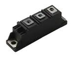
AAP Gen 7 (TO-240AA)
Power Modules Schottky Rectifier, 440 A
FEATURES
• 150 °C TJ operation
• Low forward voltage drop
• High frequency operation
• Low thermal resistance
• UL approved file E78996
• Designed and qualified for industrial level
• Material categorization: for definitions of compliance
please see www.vishay.com/doc?99912
AAP Gen 7 (TO-240AA)
BENEFITS
• Excellent thermal performances obtained by the usage of
exposed direct bonded copper substrate
PRIMARY CHARACTERISTICS
IF(AV)
440 A
• High surge capability
VR
30 V
• Easy mounting on heatsink
Package
AAP Gen 7 (TO-240AA)
Circuit configuration
Two diodes common anode
MECHANICAL DESCRIPTION
The AAP Gen 7, new generation of ADD-A-PAK module,
combines the excellent thermal performances obtained by
the usage of exposed direct bonded copper substrate, with
advanced compact simple package solution and simplified
internal structure with minimized number of interfaces.
ELECTRICAL DESCRIPTION / APPLICATIONS
The VS-VSKJS440/030 Schottky rectifier common anode
has been optimized for low reverse leakage at high
temperature. The proprietary barrier technology allows for
reliable operation up to 150 °C junction temperature.
Typical applications are in high current switching power
supplies, plating power supplies, UPS systems, converters,
freewheeling diodes, welding, and reverse battery
protection.
MAJOR RATINGS AND CHARACTERISTICS
SYMBOL
IF(AV)
CHARACTERISTICS
Rectangular waveform
VRRM
IFSM
tp = 5 μs sine
VF
200 Apk, TJ = 125 °C
TJ
Range
VALUES
UNITS
440
A
30
V
27 000
A
0.61
V
-55 to +150
°C
VOLTAGE RATINGS
PARAMETER
Maximum DC reverse voltage
Maximum working peak reverse voltage
SYMBOL
VR
VRWM
VS-VSKJS440/030
UNITS
30
V
Revision: 03-May-17
Document Number: 94645
1
For technical questions within your region: DiodesAmericas@vishay.com, DiodesAsia@vishay.com, DiodesEurope@vishay.com
THIS DOCUMENT IS SUBJECT TO CHANGE WITHOUT NOTICE. THE PRODUCTS DESCRIBED HEREIN AND THIS DOCUMENT
ARE SUBJECT TO SPECIFIC DISCLAIMERS, SET FORTH AT www.vishay.com/doc?91000
�VS-VSKJS440/030
www.vishay.com
Vishay Semiconductors
ABSOLUTE MAXIMUM RATINGS
PARAMETER
Maximum average
forward current
SYMBOL
per module
per leg
IF(AV)
TEST CONDITIONS
50 % duty cycle at TC = 97 °C, rectangular waveform
5 μs sine or 3 μs rect. pulse
Following any rated
load condition and with
rated VRRM applied
VALUES
UNITS
440
220
27 000
A
Maximum peak one cycle
non-repetitive surge current
IFSM
Non-repetitive avalanche energy
EAS
TJ = 25 °C, IAS = 20 A, L = 1 mH
198
mJ
Repetitive avalanche current
IAR
Current decaying linearly to zero in 1 μs
Frequency limited by TJ maximum VA = 1.5 x VR typical
44
A
SYMBOL
TEST CONDITIONS
VALUES
UNITS
10 ms sine or 6 ms rect. pulse
3000
ELECTRICAL SPECIFICATIONS
PARAMETER
220 A
Maximum forward voltage drop
VFM
440 A
220 A
440 A
Maximum reverse leakage current
IRM
Maximum junction capacitance
CT
Typical series inductance
LS
Maximum voltage rate of change
dV/dt
Maximum RMS insulation voltage
VINS
TJ = 25 °C
TJ = 125 °C
TJ = 25 °C
TJ = 125 °C
VR = Rated VR
VR = 5 VDC (test signal range 100 kHz to 1 MHz), 25 °C
Measured lead to lead 5 mm from package body
Rated VR
50 Hz
0.68
1.0
0.61
V
0.93
20
1120
14 800
mA
pF
5.0
nH
10 000
V/μs
3000 (1 min)
3600 (1 s)
V
VALUES
UNITS
-55 to +150
°C
THERMAL - MECHANICAL SPECIFICATIONS
PARAMETER
SYMBOL
Maximum junction and storage
temperature range
TEST CONDITIONS
TJ, TStg
Maximum thermal resistance,
junction to case per leg
RthJC
Typical thermal resistance,
case to heatsink per module
RthCS
DC operation
°C/W
0.1
Approximate weight
Mounting torque ± 10 %
to
heatsink
busbar
Case style
0.26
A mounting compound is recommended and the torque
should be rechecked after a period of 3 h to allow for the
spread of the compound.
JEDEC®
75
g
2.7
oz.
4
Nm
3
TO-240AA compatible
Revision: 03-May-17
Document Number: 94645
2
For technical questions within your region: DiodesAmericas@vishay.com, DiodesAsia@vishay.com, DiodesEurope@vishay.com
THIS DOCUMENT IS SUBJECT TO CHANGE WITHOUT NOTICE. THE PRODUCTS DESCRIBED HEREIN AND THIS DOCUMENT
ARE SUBJECT TO SPECIFIC DISCLAIMERS, SET FORTH AT www.vishay.com/doc?91000
�VS-VSKJS440/030
Vishay Semiconductors
1000
10 000
IR - Reverse Current (mA)
IF - Instantaneous Forward Current (A)
www.vishay.com
100
TJ = 150 °C
10
TJ = 125 °C
TJ = 25 °C
1
0.0
TJ = 150 °C
1000
125 °C
100
100 °C
10
75 °C
50 °C
1
25 °C
0.1
0.01
0.2
0.4
0.6
0.8
1.0
1.2
0
1.4
5
10
15
20
25
30
VFM - Forward Voltage Drop (V)
VR - Reverse Voltage (V)
Fig. 1 - Maximum Forward Voltage Drop Characteristics
Fig. 2 - Typical Values of Reverse Current vs. Reverse Voltage
CT - Junction Capacitance (pF)
100 000
TJ = 25 °C
10 000
1000
0
5
10
15
20
25
30
35
VR - Reverse Voltage (V)
ZthJC - Thermal Impedance (°C/W)
Fig. 3 - Typical Junction Capacitance vs. Reverse Voltage
1
0.1
D = 0.75
D = 0.5
D = 0.33
D = 0.25
D = 0.2
0.01
0.001
1E-05
Single Pulse
(Thermal Resistance)
1E-04
1E-03
1E-02
1E-01
1E+00
1E+01
1E+02
t1 - Rectangular Pulse Duration (s)
Fig. 4 - Maximum Thermal Impedance ZthJC Characteristics
Revision: 03-May-17
Document Number: 94645
3
For technical questions within your region: DiodesAmericas@vishay.com, DiodesAsia@vishay.com, DiodesEurope@vishay.com
THIS DOCUMENT IS SUBJECT TO CHANGE WITHOUT NOTICE. THE PRODUCTS DESCRIBED HEREIN AND THIS DOCUMENT
ARE SUBJECT TO SPECIFIC DISCLAIMERS, SET FORTH AT www.vishay.com/doc?91000
�VS-VSKJS440/030
Vishay Semiconductors
200
160
Square wave (D = 0.50)
80 % rated VRRM applied
Average Power Loss (W)
Allowable Case Temperature (°C)
www.vishay.com
120
DC
80
40
D = 0.75
D = 0.50
D = 0.33
D = 0.25
D = 0.20
150
RMS limit
100
50
DC
see note (1)
0
0
0
100
200
300
400
500
0
600
50
100
150
200
250
300
IF(AV) - Average Forward Current (A)
Fig. 5 - Maximum Allowable Case Temperature vs.
Average Forward Current
Fig. 6 - Forward Power Loss Characteristics
IFSM - Non-Repetitive Surge Current (A)
IF(AV) - Average Forward Current (A)
100 000
At Any Rated Load Condition
And With Rated VRRM Applied
Following Surge
10 000
1000
10
100
1000
10 000
tp - Square Wave Pulse Duration (μs)
Fig. 7 - Maximum Non-Repetitive Surge Current
L
D.U.T.
IRFP460
Rg = 25 Ω
Current
monitor
High-speed
switch
Freewheel
diode
+ Vd = 25 V
40HFL40S02
Fig. 8 - Unclamped Inductive Test Circuit
Note
(1) Formula used: T = T - (Pd + Pd
C
J
REV) x RthJC;
Pd = forward power loss = IF(AV) x VFM at (IF(AV)/D) (see fig. 6);
PdREV = inverse power loss = VR1 x IR (1 - D); IR at VR1 = 80 % rated VR
Revision: 03-May-17
Document Number: 94645
4
For technical questions within your region: DiodesAmericas@vishay.com, DiodesAsia@vishay.com, DiodesEurope@vishay.com
THIS DOCUMENT IS SUBJECT TO CHANGE WITHOUT NOTICE. THE PRODUCTS DESCRIBED HEREIN AND THIS DOCUMENT
ARE SUBJECT TO SPECIFIC DISCLAIMERS, SET FORTH AT www.vishay.com/doc?91000
�VS-VSKJS440/030
www.vishay.com
Vishay Semiconductors
ORDERING INFORMATION TABLE
Device code
VS-VS
KJ
S
44
0
1
2
3
4
5
/
030
6
1
-
Vishay Semiconductors product
2
-
Circuit configuration:
KJ = ADD-A-PAK - 2 diodes common anode
3
-
S = Schottky diode
4
-
Average rating (x 10)
5
-
Product silicon identification
6
-
Voltage rating (030 = 30 V)
CIRCUIT CONFIGURATION
(1)
-
(2)
+
(3)
+
LINKS TO RELATED DOCUMENTS
Dimensions
www.vishay.com/doc?95369
Revision: 03-May-17
Document Number: 94645
5
For technical questions within your region: DiodesAmericas@vishay.com, DiodesAsia@vishay.com, DiodesEurope@vishay.com
THIS DOCUMENT IS SUBJECT TO CHANGE WITHOUT NOTICE. THE PRODUCTS DESCRIBED HEREIN AND THIS DOCUMENT
ARE SUBJECT TO SPECIFIC DISCLAIMERS, SET FORTH AT www.vishay.com/doc?91000
�Outline Dimensions
Vishay Semiconductors
ADD-A-PAK Generation VII - Diode
DIMENSIONS in millimeters (inches)
29 ± 0.5
(1 ± 0.020)
30 ± 0.5
(1.18 ± 0.020)
35 REF.
18 (0.7) REF.
24 ± 0.5
(1 ± 0.020)
6.7 ± 0.3 (0.26 ± 0.012)
Viti M5 x 0.8
Screws M5 x 0.8
Document Number: 95369
Revision: 11-Nov-08
7 6
4 5
3
2
1
6.3 ± 0.2 (0.248 ± 0.008)
22.6 ± 0.2
(0.89 ± 0.008)
80 ± 0.3 (3.15 ± 0.012)
15 ± 0.5 (0.59 ± 0.020)
20 ± 0.5 (0.79 ± 0.020)
20 ± 0.5 (0.79 ± 0.020)
92 ± 0.75 (3.6 ± 0.030)
For technical questions, contact: indmodules@vishay.com
www.vishay.com
1
�Legal Disclaimer Notice
www.vishay.com
Vishay
Disclaimer
ALL PRODUCT, PRODUCT SPECIFICATIONS AND DATA ARE SUBJECT TO CHANGE WITHOUT NOTICE TO IMPROVE
RELIABILITY, FUNCTION OR DESIGN OR OTHERWISE.
Vishay Intertechnology, Inc., its affiliates, agents, and employees, and all persons acting on its or their behalf (collectively,
“Vishay”), disclaim any and all liability for any errors, inaccuracies or incompleteness contained in any datasheet or in any other
disclosure relating to any product.
Vishay makes no warranty, representation or guarantee regarding the suitability of the products for any particular purpose or
the continuing production of any product. To the maximum extent permitted by applicable law, Vishay disclaims (i) any and all
liability arising out of the application or use of any product, (ii) any and all liability, including without limitation special,
consequential or incidental damages, and (iii) any and all implied warranties, including warranties of fitness for particular
purpose, non-infringement and merchantability.
Statements regarding the suitability of products for certain types of applications are based on Vishay's knowledge of typical
requirements that are often placed on Vishay products in generic applications. Such statements are not binding statements
about the suitability of products for a particular application. It is the customer's responsibility to validate that a particular product
with the properties described in the product specification is suitable for use in a particular application. Parameters provided in
datasheets and / or specifications may vary in different applications and performance may vary over time. All operating
parameters, including typical parameters, must be validated for each customer application by the customer's technical experts.
Product specifications do not expand or otherwise modify Vishay's terms and conditions of purchase, including but not limited
to the warranty expressed therein.
Hyperlinks included in this datasheet may direct users to third-party websites. These links are provided as a convenience and
for informational purposes only. Inclusion of these hyperlinks does not constitute an endorsement or an approval by Vishay of
any of the products, services or opinions of the corporation, organization or individual associated with the third-party website.
Vishay disclaims any and all liability and bears no responsibility for the accuracy, legality or content of the third-party website
or for that of subsequent links.
Except as expressly indicated in writing, Vishay products are not designed for use in medical, life-saving, or life-sustaining
applications or for any other application in which the failure of the Vishay product could result in personal injury or death.
Customers using or selling Vishay products not expressly indicated for use in such applications do so at their own risk. Please
contact authorized Vishay personnel to obtain written terms and conditions regarding products designed for such applications.
No license, express or implied, by estoppel or otherwise, to any intellectual property rights is granted by this document or by
any conduct of Vishay. Product names and markings noted herein may be trademarks of their respective owners.
© 2023 VISHAY INTERTECHNOLOGY, INC. ALL RIGHTS RESERVED
Revision: 01-Jan-2023
1
Document Number: 91000
�