VS-VSKT500-..PbF, VS-VSKH500-..PbF, VS-VSKL500-..PbF Series
www.vishay.com
Vishay Semiconductors
Thyristor/Diode and Thyristor/Thyristor
(Super MAGN-A-PAK Power Modules), 500 A
FEATURES
• High current capability
• High surge capability
• Industrial standard package
• 3000 VRMS isolating voltage with non-toxic
substrate
• UL approved file E78996
• Designed and qualified for industrial level
• Material categorization: for definitions of compliance
please see www.vishay.com/doc?99912
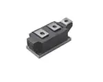
Super MAGN-A-PAK
TYPICAL APPLICATIONS
• Motor starters
• DC motor controls - AC motor controls
PRIMARY CHARACTERISTICS
IT(AV), IF(AV)
500 A
Type
Modules - thyristor, standard
Package
Super MAGN-A-PAK
• Uninterruptible power supplies
MAJOR RATINGS AND CHARACTERISTICS
SYMBOL
CHARACTERISTICS
VALUES
UNITS
500
A
TC = 82 °C
785
A
50 Hz
17.8
60 Hz
18.7
50 Hz
1591
60 Hz
1452
IT(AV) , IF(AV)
TC = 82 °C
IT(RMS)
ITSM
I2t
I2t
kA
kA2s
15 910
kA2s
V
VRRM
Range
800 to 1600
TStg
Range
-40 to +150
TJ
Range
-40 to +130
°C
ELECTRICAL SPECIFICATIONS
VOLTAGE RATINGS
TYPE NUMBER
VS-VSK.500
VOLTAGE
CODE
VRRM/VDRM, MAXIMUM REPETITIVE
PEAK REVERSE VOLTAGE
V
VRSM, MAXIMUM NON-REPETITIVE
PEAK REVERSE VOLTAGE
V
08
800
900
12
1200
1300
14
1400
1500
16
1600
1700
IRRM/IDRM MAXIMUM
AT TJ = TJ MAXIMUM
mA
100
Revision: 26-Jul-2018
Document Number: 94420
1
For technical questions within your region: DiodesAmericas@vishay.com, DiodesAsia@vishay.com, DiodesEurope@vishay.com
THIS DOCUMENT IS SUBJECT TO CHANGE WITHOUT NOTICE. THE PRODUCTS DESCRIBED HEREIN AND THIS DOCUMENT
ARE SUBJECT TO SPECIFIC DISCLAIMERS, SET FORTH AT www.vishay.com/doc?91000
�VS-VSKT500-..PbF, VS-VSKH500-..PbF, VS-VSKL500-..PbF Series
www.vishay.com
Vishay Semiconductors
ON-STATE CONDUCTION
PARAMETER
SYMBOL
TEST CONDITIONS
VALUES
UNITS
500
A
Maximum average on-state current
at case temperature
IT(AV),
IF(AV)
180° conduction, half sine wave
82
°C
Maximum RMS on-state current
IT(RMS)
180° conduction, half sine wave at TC = 82 °C
785
A
t = 10 ms
No voltage
reapplied
17.8
100 % VRRM
reapplied
15.0
Maximum peak, one-cycle,
non-repetitive on-state surge current
ITSM,
IFSM
t = 8.3 ms
t = 10 ms
t = 8.3 ms
t = 10 ms
Maximum I2t for fusing
I2t
Maximum I2t for fusing
I2t
t = 8.3 ms
t = 10 ms
t = 8.3 ms
No voltage
reapplied
18.7
Sinusoidal
half wave,
initial TJ = TJ maximum
100 % VRRM
reapplied
t = 0.1 ms to 10 ms, no voltage reapplied
kA
15.7
1591
1452
1125
kA2s
1027
15 910
Low level value or threshold voltage
VT(TO)1
(16.7 % x x IT(AV) < I < x IT(AV)), TJ = TJ maximum
0.85
High level value of threshold voltage
VT(TO)2
(I > x IT(AV)), TJ = TJ maximum
0.93
Low level value on-state slope resistance
rt1
(16.7 % x x IT(AV) < I < x IT(AV)), TJ = TJ maximum
0.36
High level value on-state slope resistance
rt2
(I > x IT(AV)), TJ = TJ maximum
0.32
kA2s
V
m
Maximum on-state voltage drop
VTM
Ipk = 1500 A, TJ = 25 °C, tp = 10 ms sine pulse
1.50
V
Maximum forward voltage drop
VFM
Ipk = 1500 A, TJ = 25 °C, tp = 10 ms sine pulse
1.50
V
Maximum holding current
IH
Maximum latching current
IL
TJ = 25 °C, anode supply 12 V resistive load
500
1000
mA
SWITCHING
PARAMETER
Maximum rate of rise of turned-on current
SYMBOL
dI/dt
TEST CONDITIONS
TJ = TJ maximum, ITM = 400 A, VDRM applied
VALUES
UNITS
1000
A/μs
Typical delay time
td
Gate current 1 A, dIg/dt = 1 A/μs
Vd = 0.67 % VDRM, TJ = 25 °C
2.0
Typical turn-off time
tq
ITM = 750 A; TJ = TJ maximum, dI/dt = - 60 A/μs,
VR = 50 V, dV/dt = 20 V/μs, gate 0 V 100
200
μs
BLOCKING
PARAMETER
Maximum critical rate of rise
of off-state voltage
SYMBOL
dV/dt
TEST CONDITIONS
VALUES
UNITS
TJ = 130 °C, linear to VD = 80 % VDRM
1000
V/μs
RMS insulation voltage
VINS
t=1s
3000
V
Maximum peak reverse and
off-state leakage current
IRRM,
IDRM
TJ = TJ maximum, rated VDRM/VRRM applied
100
mA
Revision: 26-Jul-2018
Document Number: 94420
2
For technical questions within your region: DiodesAmericas@vishay.com, DiodesAsia@vishay.com, DiodesEurope@vishay.com
THIS DOCUMENT IS SUBJECT TO CHANGE WITHOUT NOTICE. THE PRODUCTS DESCRIBED HEREIN AND THIS DOCUMENT
ARE SUBJECT TO SPECIFIC DISCLAIMERS, SET FORTH AT www.vishay.com/doc?91000
�VS-VSKT500-..PbF, VS-VSKH500-..PbF, VS-VSKL500-..PbF Series
www.vishay.com
Vishay Semiconductors
TRIGGERING
PARAMETER
SYMBOL
Maximum peak gate power
PGM
Maximum peak average gate power
PG(AV)
Maximum peak positive gate current
+IGM
Maximum peak positive gate voltage
+VGM
Maximum peak negative gate voltage
-VGM
Maximum DC gate current required to trigger
IGT
DC gate voltage required to trigger
VGT
DC gate current not to trigger
IGD
DC gate voltage not to trigger
VGD
TEST CONDITIONS
VALUES
TJ = TJ maximum, tp 5 ms
10
TJ = TJ maximum, f = 50 Hz, d% = 50
2.0
3.0
TJ = TJ maximum, tp 5 ms
20
5.0
TJ = 25 °C, Vak 12 V
TJ = TJ maximum
UNITS
W
A
V
200
mA
3.0
V
10
mA
0.25
V
VALUES
UNITS
THERMAL AND MECHANICAL SPECIFICATIONS
PARAMETER
SYMBOL
Maximum junction operating
temperature range
TEST CONDITIONS
TJ
-40 to +130
Maximum storage temperature range
TStg
-40 to +150
Maximum thermal resistance,
junction to case per junction
RthJC
Maximum thermal resistance,
case to heatsink per module
RthC-hs
0.065
Mounting surface smooth, flat and greased
0.02
K/W
Super MAGN-A-PAK to heatsink
Mounting
torque
± 10 %
DC operation
°C
busbar to super MAGN-A-PAK
A mounting compound is recommended and
the torque should be rechecked after a period
of 3 hours to allow for the spread of the
compound
Approximate weight
6 to 8
Nm
12 to 15
1500
Case style
See dimensions - link at the end of datasheet
g
Super MAGN-A-PAK
RthJC CONDUCTION
CONDUCTION ANGLE
SINUSOIDAL CONDUCTION
RECTANGULAR CONDUCTION
180°
0.009
0.006
120°
0.011
0.011
90°
0.014
0.015
60°
0.021
0.022
30°
0.037
0.038
TEST CONDITIONS
UNITS
TJ = TJ maximum
K/W
Note
• Table shows the increment of thermal resistance RthJC when devices operate at different conduction angles than DC
Revision: 26-Jul-2018
Document Number: 94420
3
For technical questions within your region: DiodesAmericas@vishay.com, DiodesAsia@vishay.com, DiodesEurope@vishay.com
THIS DOCUMENT IS SUBJECT TO CHANGE WITHOUT NOTICE. THE PRODUCTS DESCRIBED HEREIN AND THIS DOCUMENT
ARE SUBJECT TO SPECIFIC DISCLAIMERS, SET FORTH AT www.vishay.com/doc?91000
�VS-VSKT500-..PbF, VS-VSKH500-..PbF, VS-VSKL500-..PbF Series
130
VSK.500.. Series
R thJC (DC) = 0.065 K/ W
120
110
Conduc tion Angle
100
90
30°
80
60°
90°
120°
70
180°
60
0
100
200
300
400
500
600
Maximum Average On-state Power Loss (W)
Vishay Semiconductors
DC
180°
120°
90°
60°
30°
900
800
700
600
500
400 RMS Limit
Conduction Period
300
VSK.500.. Series
Per Junc tion
TJ = 130°C
200
100
0
0
100 200 300 400 500 600 700 800
Average On-state Current (A)
Average On-state Current (A)
Fig. 4 - On-State Power Loss Characteristics
130
VSK.500.. Series
R thJC (DC) = 0.065 K/ W
120
110
Conduction Period
100
90
80
30°
60°
90°
120°
180°
70
DC
60
0
180°
120°
90°
60°
30°
400
RMSLimit
300
Conduc tion Angle
200
VSK.500.. Series
Per Junction
TJ= 130°C
100
0
0
14000
100
200
300
400
@60 Hz 0.0083 s
@50 Hz 0.0100 s
13000
12000
11000
10000
9000
VSK.500.. Series
Per Junction
8000
7000
1
10
100
Fig. 5 - Maximum Non-Repetitive Surge Current
500
Average On-state Current (A)
Fig. 3 - On-State Power Loss Characteristics
Peak Half Sine Wave On-state Current (A)
700
500
At Any Rated Loa d Cond ition And With
Rated VRRM Ap p lied Following Surge.
Initial TJ = 130°C
15000
Number Of Equal Amplitude Half Cycle Current Pulses (N)
Fig. 2 - Current Ratings Characteristics
600
16000
100 200 300 400 500 600 700 800 900
Average On-state Current (A)
Maximum Average On-state Power Loss (W)
1000
Fig. 1 - Current Ratings Characteristics
Peak Half Sine Wave On-state Current (A)
Maximum Allowable Case Temperature (°C)
Maximum Allowable Case Temperature (°C)
www.vishay.com
18000
16000
14000
Ma ximum Non Rep etitive Surge Current
Versus Pulse Train Dura tion. Control
Of Cond uc tion Ma y Not Be Maintained.
Initial TJ = 130°C
No Voltage Reapplied
Rated VRRMReapplied
12000
10000
8000
VSK.500.. Series
Per Junction
6000
0.01
0.1
1
Pulse Train Duration (s)
Fig. 6 - Maximum Non-Repetitive Surge Current
Revision: 26-Jul-2018
Document Number: 94420
4
For technical questions within your region: DiodesAmericas@vishay.com, DiodesAsia@vishay.com, DiodesEurope@vishay.com
THIS DOCUMENT IS SUBJECT TO CHANGE WITHOUT NOTICE. THE PRODUCTS DESCRIBED HEREIN AND THIS DOCUMENT
ARE SUBJECT TO SPECIFIC DISCLAIMERS, SET FORTH AT www.vishay.com/doc?91000
�VS-VSKT500-..PbF, VS-VSKH500-..PbF, VS-VSKL500-..PbF Series
Vishay Semiconductors
=
W
K/
W
K/
SA
R th
09
0.
750
700
180°
650
120°
0.
16
90°
600
K/
60°
W
550
0.2
30°
K/
500 Conduction Angle
W
450
400
0.3
K/ W
350
0
.4 K
300
/W
250
0.6 K
200
/W
150
VSK.500.. Series
Per Module
100
TJ = 130°C
50
0
0 100 200 300 400 500 600 700 800
0
20
12
0.
07
0.
W
K/
e lt
-D
a
R
Maximum Total On-state Power Loss (W)
www.vishay.com
40
60
80
100
120
Maximum Allowable Ambient Temperature (°C)
Total RMSOutput Current (A)
Fig. 7 - On-State Power Loss Characteristics
0.
02
K/
W
1000
0.0
8K
/W
0.12
K/ W
0.2 K
/W
2 x VSK.500.. Series
Single Phase Bridge
Connected
T J = 130°C
500
R
K/
W
ta
el
-D
1500
W
K/
0.0
5
01
0.
2000
K/
W
=
0.
03
A
hS
180°
(Sine)
180°
(Rect)
2500
Rt
Maximum Total Power Loss (W)
3000
0
0
200
400
600
800
0
1000
Total Output Current (A)
20
40
60
80
100
120
Maximum Allowable Ambient Temperature (°C)
Fig. 8 - On-State Power Loss Characteristics
R
4000
120°
(Rect)
3500
SA
th
Maximum Total Power Loss (W)
4500
0.
02
K/
W
0.0
3K
/W
3000
2500
2000
1500
3 x VSK.500.. Series
Three Phase Bridge
Connected
T J = 130°C
1000
500
=
0.
01
K/
W
-D
el
ta
R
0.0
5K
/W
0.08
K/ W
0.2 K/
W
0
0
250
500
750
0
1000 1250 1500
Total Output Current (A)
20
40
60
80
100
120
Maximum Allowable Ambient Temperature (°C)
Fig. 9 - On-State Power Loss Characteristics
Revision: 26-Jul-2018
Document Number: 94420
5
For technical questions within your region: DiodesAmericas@vishay.com, DiodesAsia@vishay.com, DiodesEurope@vishay.com
THIS DOCUMENT IS SUBJECT TO CHANGE WITHOUT NOTICE. THE PRODUCTS DESCRIBED HEREIN AND THIS DOCUMENT
ARE SUBJECT TO SPECIFIC DISCLAIMERS, SET FORTH AT www.vishay.com/doc?91000
�VS-VSKT500-..PbF, VS-VSKH500-..PbF, VS-VSKL500-..PbF Series
www.vishay.com
Vishay Semiconductors
Transient Thermal Impedance Z thJC (K/ W)
Instantaneous On-state Current (A)
10000
TJ= 25°C
1000
TJ= 130°C
VSK.500.. Series
Per Junction
100
0.5
1
1.5
2
2.5
3
3.5
4
4.5
0.1
VSK.500.. Series
Per Junc tion
0.01
Steady State Value:
RthJC = 0.065 K/ W
(DC Operation)
0.001
0.001
0.01
0.1
1
10
100
Instantaneous On-state Voltage (V)
Square Wave Pulse Duration (s)
Fig. 10 - On-State Voltage Drop Characteristics
Fig. 11 - Thermal Impedance ZthJC Characteristics
Rectangular gate pulse
a) Recommended load line for
rated di/ dt : 20V, 10ohms; tr