VSMY1850
www.vishay.com
Vishay Semiconductors
High Speed Infrared Emitting Diodes, 850 nm,
Surface Emitter Technology
FEATURES
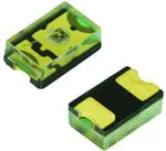
• Package type: surface mount
• Package form: 0805
• Dimensions (L x W x H in mm): 2 x 1.25 x 0.85
• Peak wavelength: λp = 850 nm
• High reliability
• High radiant power
• High radiant intensity
• High speed
• Angle of half sensitivity: ϕ = ± 60°
• Suitable for high pulse current operation
21531
• 0805 standard surface-mountable package
• Floor life: 168 h, MSL 3, according to J-STD-020
• Lead (Pb)-free reflow soldering
DESCRIPTION
• Material categorization: for definitions of compliance
please see www.vishay.com/doc?99912
As part of the SurfLightTM portfolio, the VSMY1850 is an
infrared, 850 nm emitting diode based on GaAlAs surface
emitter chip technology with high radiant intensity, high
optical power and high speed, molded in clear, untinted
0805 plastic package for surface mounting (SMD).
APPLICATIONS
• IrDA compatible data transmission
• Miniature light barrier
• Photointerrupters
• Optical switch
• Emitter source for proximity sensors
• IR touch panels
• IR Flash
• IR illumination
• 3D TV
PRODUCT SUMMARY
COMPONENT
Ie (mW/sr)
ϕ (deg)
λp (nm)
tr (ns)
10
± 60
850
10
VSMY1850
Note
• Test conditions see table “Basic Characteristics“
ORDERING INFORMATION
ORDERING CODE
PACKAGING
REMARKS
PACKAGE FORM
VSMY1850
Tape and reel
MOQ: 3000 pcs, 3000 pcs/reel
0805
Note
• MOQ: minimum order quantity
Rev. 1.5, 30-Jun-16
Document Number: 83397
1
For technical questions, contact: emittertechsupport@vishay.com
THIS DOCUMENT IS SUBJECT TO CHANGE WITHOUT NOTICE. THE PRODUCTS DESCRIBED HEREIN AND THIS DOCUMENT
ARE SUBJECT TO SPECIFIC DISCLAIMERS, SET FORTH AT www.vishay.com/doc?91000
�VSMY1850
www.vishay.com
Vishay Semiconductors
ABSOLUTE MAXIMUM RATINGS (Tamb = 25 °C, unless otherwise specified)
PARAMETER
TEST CONDITION
SYMBOL
VALUE
UNIT
VR
5
V
Reverse voltage
Forward current
IF
100
mA
Peak forward current
tp/T = 0.5, tp = 100 μs
IFM
200
mA
Surge forward current
tp = 100 μs
IFSM
1
A
PV
190
mW
°C
Power dissipation
Junction temperature
Tj
100
Operating temperature range
Tamb
-40 to +85
°C
Storage temperature range
Tstg
-40 to +100
°C
According to Fig. 7, J-STD-020
Tsd
260
°C
JESD 51
RthJA
270
K/W
Soldering temperature
Thermal resistance junction / ambient
120
100
IF - Forward Current (mA)
PV - Power Dissipation (mW)
200
160
120
RthJA = 270 K/W
80
40
80
60
RthJA = 270 K/W
40
20
0
0
0
22108
20
40
60
80
0
100
Tamb - Ambient Temperature (°C)
20
Fig. 1 - Power Dissipation Limit vs. Ambient Temperature
40
60
80
100
Tamb - Ambient Temperature (°C)
22109
Fig. 2 - Forward Current Limit vs. Ambient Temperature
BASIC CHARACTERISTICS (Tamb = 25 °C, unless otherwise specified)
PARAMETER
Forward voltage
Temperature coefficient of VF
TEST CONDITION
SYMBOL
MIN.
TYP.
MAX.
UNIT
IF = 100 mA, tp = 20 ms
VF
-
1.65
1.9
V
IF = 1 A, tp = 100 μs
VF
-
2.9
-
V
IF = 1 mA
TKVF
-
-1.4
-
mV/K
IF = 10 mA
TKVF
-
-1.18
-
mV/K
Reverse current
Junction capacitance
IR
VR = 0 V, f = 1 MHz,
E = 0 mW/cm2
Not designed for reverse operation
125
-
pF
5
10
15
mW/sr
-
85
-
mW/sr
φe
-
50
-
mW
IF = 100 mA
TKφe
-
-0.35
-
%/K
ϕ
-
± 60
-
deg
Peak wavelength
IF = 100 mA
λp
840
850
870
nm
Spectral bandwidth
IF = 30 mA
Δλ
-
30
-
nm
Temperature coefficient of λp
IF = 30 mA
TKλp
-
0.25
-
nm/K
Rise time
IF = 100 mA, 20 % to 80 %
tr
-
10
-
ns
Fall time
IF = 100 mA, 20 % to 80 %
tf
-
10
-
ns
d
-
0.5
-
mm
Radiant intensity
Radiant power
Temperature coefficient of radiant
power
CJ
-
IF = 100 mA, tp = 20 ms
Ie
IF = 1 A, tp = 100 μs
Ie
IF = 100 mA, tp = 20 ms
μA
Angle of half intensity
Virtual source diameter
Rev. 1.5, 30-Jun-16
Document Number: 83397
2
For technical questions, contact: emittertechsupport@vishay.com
THIS DOCUMENT IS SUBJECT TO CHANGE WITHOUT NOTICE. THE PRODUCTS DESCRIBED HEREIN AND THIS DOCUMENT
ARE SUBJECT TO SPECIFIC DISCLAIMERS, SET FORTH AT www.vishay.com/doc?91000
�VSMY1850
www.vishay.com
Vishay Semiconductors
BASIC CHARACTERISTICS (Tamb = 25 °C, unless otherwise specified)
10
Φe, rel - Relative Radiant Power
1
1
0.1
0.01
IF = 30 mA
0.75
0.5
0.25
0.001
0
0.5
1
1.5
2
2.5
3
VF - Forward Voltage (V)
22097
0
650
3.5
750
Fig. 3 - Forward Current vs. Forward Voltage
850
Fig. 5 - Relative Radiant Power vs. Wavelength
0°
10°
20°
30°
Ie, rel - Relative Radiant Intensity
Ie - Radiant Intensity (mW/sr)
1000
100
tp = 100 µs
10
1
0.1
0.001
0.01
0.1
1
40°
1.0
0.9
50°
0.8
60°
70°
0.7
80°
0.6
0.4
0.2
0
948013-1
IF - Forward Current (A)
22110
Fig. 4 - Radiant Intensity vs. Forward Current
REFLOW SOLDER PROFILE
max. 260 °C
245 °C
255 °C
240 °C
217 °C
250
Time between soldering and removing from MBB must not
exceed the time indicated in J-STD-020:
max. 30 s
150
max. 100 s
max. 120 s
Moisture sensitivity: level 3
100
max. ramp down 6 °C/s
0
19841
50
100
150
200
250
300
Time (s)
Fig. 7 - Lead (Pb)-free Reflow Solder Profile
According to J-STD-020
Rev. 1.5, 30-Jun-16
Floor life: 168 h
Conditions: Tamb < 30 °C, RH < 60 %
max. ramp up 3 °C/s
0
Devices are packed in moisture barrier bags (MBB) to
prevent the products from moisture absorption during
transportation and storage. Each bag contains a desiccant.
FLOOR LIFE
200
50
Fig. 6 - Relative Radiant Intensity vs. Angular Displacement
DRYPACK
300
Temperature (°C)
950
λ - Wavelength (nm)
21776-1
ϕ - Angular Displacement
IF - Forward Current (A)
tp = 100 µs
DRYING
In case of moisture absorption devices should be baked
before soldering. Conditions see J-STD-020 or label.
Devices taped on reel dry using recommended conditions
192 h at 40 °C (+ 5 °C), RH < 5 %.
Document Number: 83397
3
For technical questions, contact: emittertechsupport@vishay.com
THIS DOCUMENT IS SUBJECT TO CHANGE WITHOUT NOTICE. THE PRODUCTS DESCRIBED HEREIN AND THIS DOCUMENT
ARE SUBJECT TO SPECIFIC DISCLAIMERS, SET FORTH AT www.vishay.com/doc?91000
�VSMY1850
www.vishay.com
Vishay Semiconductors
PACKAGE DIMENSIONS in millimeters
Cathode
Bottom view
Anode
1
technical drawings
specifications
according to DIN
Not indicated tolerances ± 0.1
Side View
0.35
0.85
2
0.6
0.6
Top View
1.25
Recommended solder pad
footprint
1
0.625
1
1.2
0.82
0.6
Drawing-No.: 6.541-5083.01-4
Issue: 2; 10.09.2013
Rev. 1.5, 30-Jun-16
Document Number: 83397
4
For technical questions, contact: emittertechsupport@vishay.com
THIS DOCUMENT IS SUBJECT TO CHANGE WITHOUT NOTICE. THE PRODUCTS DESCRIBED HEREIN AND THIS DOCUMENT
ARE SUBJECT TO SPECIFIC DISCLAIMERS, SET FORTH AT www.vishay.com/doc?91000
�VSMY1850
www.vishay.com
Vishay Semiconductors
BLISTER TAPE DIMENSIONS in millimeters
4
Ø 1.55 ± 0.05
0.2 ± 0.05
2 ± 0.05
8
2.24
3.5 ± 0.05
1.75
Anode
0.94
Cathode
1.45
4
Ø 1.1 + 0.1
Not indicated tolerances ±0.1
Reel off direction
Drawing-No.: 9.700-5352.01-4
Issue: 1; 13.04.10
technical drawings
according to DIN
specifications
22112
REEL DIMENSIONS in millimeters
8.4 +2.5
Ø 177.8 max.
Ø 55 min.
8.4 +0.15
Z
Form of the leave open
of the wheel is supplier specific.
14.4 max.
Ø 20.2 min.
1.5 min.
Ø 13 - 0.2
+ 0.5
Z 2:1
Drawing-No.: 9.800-5096.01-4
Issue: 2; 26.04.10
20875
Rev. 1.5, 30-Jun-16
technical drawings
according to DIN
specifications
Document Number: 83397
5
For technical questions, contact: emittertechsupport@vishay.com
THIS DOCUMENT IS SUBJECT TO CHANGE WITHOUT NOTICE. THE PRODUCTS DESCRIBED HEREIN AND THIS DOCUMENT
ARE SUBJECT TO SPECIFIC DISCLAIMERS, SET FORTH AT www.vishay.com/doc?91000
�Legal Disclaimer Notice
www.vishay.com
Vishay
Disclaimer
ALL PRODUCT, PRODUCT SPECIFICATIONS AND DATA ARE SUBJECT TO CHANGE WITHOUT NOTICE TO IMPROVE
RELIABILITY, FUNCTION OR DESIGN OR OTHERWISE.
Vishay Intertechnology, Inc., its affiliates, agents, and employees, and all persons acting on its or their behalf (collectively,
“Vishay”), disclaim any and all liability for any errors, inaccuracies or incompleteness contained in any datasheet or in any other
disclosure relating to any product.
Vishay makes no warranty, representation or guarantee regarding the suitability of the products for any particular purpose or
the continuing production of any product. To the maximum extent permitted by applicable law, Vishay disclaims (i) any and all
liability arising out of the application or use of any product, (ii) any and all liability, including without limitation special,
consequential or incidental damages, and (iii) any and all implied warranties, including warranties of fitness for particular
purpose, non-infringement and merchantability.
Statements regarding the suitability of products for certain types of applications are based on Vishay's knowledge of typical
requirements that are often placed on Vishay products in generic applications. Such statements are not binding statements
about the suitability of products for a particular application. It is the customer's responsibility to validate that a particular product
with the properties described in the product specification is suitable for use in a particular application. Parameters provided in
datasheets and / or specifications may vary in different applications and performance may vary over time. All operating
parameters, including typical parameters, must be validated for each customer application by the customer's technical experts.
Product specifications do not expand or otherwise modify Vishay's terms and conditions of purchase, including but not limited
to the warranty expressed therein.
Hyperlinks included in this datasheet may direct users to third-party websites. These links are provided as a convenience and
for informational purposes only. Inclusion of these hyperlinks does not constitute an endorsement or an approval by Vishay of
any of the products, services or opinions of the corporation, organization or individual associated with the third-party website.
Vishay disclaims any and all liability and bears no responsibility for the accuracy, legality or content of the third-party website
or for that of subsequent links.
Except as expressly indicated in writing, Vishay products are not designed for use in medical, life-saving, or life-sustaining
applications or for any other application in which the failure of the Vishay product could result in personal injury or death.
Customers using or selling Vishay products not expressly indicated for use in such applications do so at their own risk. Please
contact authorized Vishay personnel to obtain written terms and conditions regarding products designed for such applications.
No license, express or implied, by estoppel or otherwise, to any intellectual property rights is granted by this document or by
any conduct of Vishay. Product names and markings noted herein may be trademarks of their respective owners.
© 2022 VISHAY INTERTECHNOLOGY, INC. ALL RIGHTS RESERVED
Revision: 01-Jan-2022
1
Document Number: 91000
�