VX60M100PW
www.vishay.com
Vishay General Semiconductor
Dual High Voltage TMBS® (Trench MOS Barrier Schottky) Rectifier
Ultra Low VF = 0.39 V at IF = 5.0 A
FEATURES
• Trench MOS Schottky technology
Available
• Low forward voltage drop, low power losses
• High efficiency operation
1
• Solder bath temperature 275 °C maximum,
10 s per JESD 22-B106
2
3
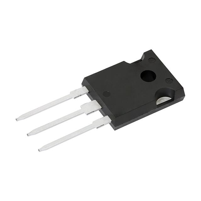
TO-247AD 3L
• AEC-Q101 qualified available:
- Automotive ordering code: base P/NHM3
PIN 1
PIN 2
PIN 3
CASE
• Material categorization: for definitions of compliance
please see www.vishay.com/doc?99912
TYPICAL APPLICATIONS
PRIMARY CHARACTERISTICS
IF(AV)
2 x 30 A
VRRM
100 V
IFSM
350 A
VF at IF = 30 A (TJ = 125 °C)
0.65 V
TJ max.
175 °C
Package
TO-247AD 3L
Circuit configuration
Common cathode
For use in high frequency DC/DC converters, switching
power supplies, freewheeling diodes, OR-ing diode, and
reverse battery protection in commercial, industrial, and
automotive application.
MECHANICAL DATA
Case: TO-247AD 3L
Molding compound meets UL 94 V-0 flammability rating
Base P/N-M3 - halogen-free, RoHS-compliant
Base P/NHM3 - halogen-free, RoHS-compliant, and
AEC-Q101 qualified
Terminals: matte tin plated
J-STD-002 and JESD 22-B102
leads,
solderable
per
Polarity: as marked
Mounting torque: 10 in-lbs maximum
MAXIMUM RATINGS (TA = 25 °C unless otherwise noted)
PARAMETER
Maximum repetitive peak reverse voltage
Maximum average forward rectified current
(fig. 1)
SYMBOL
VX60M100PW
UNIT
VRRM
100
V
per device
per diode
60
IF(AV)
A
30
Peak forward surge current 8.3 ms single half sine-wave
superimposed on rated load
IFSM
350
Operating junction temperature range
TJ (1)
-40 to +175
Storage temperature range
TSTG
-40 to +175
A
°C
Note
(1) The heat generated must be less than the thermal conductivity from junction-to-ambient: dP /dT < 1/R
D
J
θJA
Revision: 29-Jul-2020
Document Number: 87008
1
For technical questions within your region: DiodesAmericas@vishay.com, DiodesAsia@vishay.com, DiodesEurope@vishay.com
THIS DOCUMENT IS SUBJECT TO CHANGE WITHOUT NOTICE. THE PRODUCTS DESCRIBED HEREIN AND THIS DOCUMENT
ARE SUBJECT TO SPECIFIC DISCLAIMERS, SET FORTH AT www.vishay.com/doc?91000
�VX60M100PW
www.vishay.com
Vishay General Semiconductor
ELECTRICAL CHARACTERISTICS (TJ = 25 °C unless otherwise noted)
PARAMETER
TEST CONDITIONS
SYMBOL
IF = 5 A
IF = 15 A
Instantaneous forward voltage per diode
TJ = 25 °C
IF = 30 A
VF (1)
IF = 5 A
IF = 15 A
TJ = 125 °C
Reverse current at rated VR per diode
VR = 100 V
Typical junction capacitance
MAX.
0.49
-
0.61
-
0.75
0.83
0.39
-
0.54
-
0.65
0.73
TJ = 25 °C
0.0035
-
TJ = 125 °C
4
-
-
0.5
7
20
2600
-
IF = 30 A
VR = 70 V
TYP.
TJ = 25 °C
IR (2)
TJ = 125 °C
4.0 V, 1 MHz
CJ
UNIT
V
mA
pF
Notes
(1) Pulse test: 300 μs pulse width, 1 % duty cycle
(2) Pulse test: Pulse width ≤ 5 ms
THERMAL CHARACTERISTICS (TA = 25 °C unless otherwise noted)
PARAMETER
SYMBOL
Typical thermal resistance per device
RθJC
(1)
VX60M100PW
UNIT
0.6
°C/W
Note
(1) Thermal resistance junction-to-case to follow JEDEC® 51-14 transient dual interface test method (TDIM)
ORDERING INFORMATION (Example)
PREFERRED P/N
UNIT WEIGHT (g)
PACKAGE CODE
BASE QUANTITY
DELIVERY MODE
VX60M100PW-M3/P
5.64
P
25/tube
Tube
VX60M100PWHM3/P (1)
5.64
P
25/tube
Tube
Note
(1) AEC-Q101 qualified
Revision: 29-Jul-2020
Document Number: 87008
2
For technical questions within your region: DiodesAmericas@vishay.com, DiodesAsia@vishay.com, DiodesEurope@vishay.com
THIS DOCUMENT IS SUBJECT TO CHANGE WITHOUT NOTICE. THE PRODUCTS DESCRIBED HEREIN AND THIS DOCUMENT
ARE SUBJECT TO SPECIFIC DISCLAIMERS, SET FORTH AT www.vishay.com/doc?91000
�VX60M100PW
www.vishay.com
Vishay General Semiconductor
RATINGS AND CHARACTERISTICS CURVES (TA = 25 °C, unless otherwise noted)
Axis Title
Axis Title
60
50
1000
40
30
100
20
10
10
0
25
50
75
100
125
150
TJ = 150 °C
10
TJ = 125 °C
1
0.01
TJ = 25 °C
100
0.001
0.0001
TJ = -40 °C
10
0.00001
175
20
40
60
80
100
Percent of Rated Peak Reverse Voltage (%)
Fig. 4 - Typical Reverse Leakage Characteristics
Fig. 1 - Maximum Forward Current Derating Curve
Axis
Title
Axis Title
Axis Title
10 000
30.0
25.0
10000
TJ = 25 °C
f = 1.0 MHz
Vsig = 50 mVp-p
10000
D = 0.8
D = 1.0
1000
D = 0.2
15.0
D = 0.1
10.0
100
T
5.0
D = tp/T
10
15
20
25
30
100
35
10
100
10
5
1000
tp
0
0
1000
1st line
2nd line
20.0
2nd line
Junction Capacitance (pF)
D = 0.5
D = 0.3
1st line
2nd line
2nd line
Average Power Loss (W)
1000
TJ = 100 °C
0.1
Case Temperature (°C)
0.1
40
1
10
100
Average Forward Current (A)
Reverse Voltage (V)
Fig. 2 - Average Power Loss Characteristics
Fig. 5 - Typical Junction Capacitance
Axis Title
Axis Title
10000
1
TJ = 175 °C
TJ = 150 °C
1000
1st line
2nd line
10
TJ = 125 °C
TJ = 100 °C
1
100
TJ = 25 °C
TJ = -40 °C
10
0.1
0
0.1 0.2 0.3 0.4 0.5 0.6 0.7 0.8 0.9 1.0
Instantaneous Forward Voltage (V)
Fig. 3 - Typical Instantaneous Forward Characteristics
10000
2nd line
Transient Thermal Impedance (°C/W)
100
2nd line
Instantaneous Forward Current (A)
10000
TJ = 175 °C
Junction to case
1000
100
0.1
0.01
1st line
2nd line
0
2nd line
Instantaneous Reverse Current (mA)
TC = 149.8°C, R thJC = 0.6 ƱC/W
1st line
2ndline
line
2nd
2nd line
Average Forward Rectified Current (A)
100
1st line
2nd line
10000
70
10
0.1
1
10
100
t - Pulse Duration (s)
Fig. 6 - Typical Transient Thermal Impedance
Revision: 29-Jul-2020
Document Number: 87008
3
For technical questions within your region: DiodesAmericas@vishay.com, DiodesAsia@vishay.com, DiodesEurope@vishay.com
THIS DOCUMENT IS SUBJECT TO CHANGE WITHOUT NOTICE. THE PRODUCTS DESCRIBED HEREIN AND THIS DOCUMENT
ARE SUBJECT TO SPECIFIC DISCLAIMERS, SET FORTH AT www.vishay.com/doc?91000
�VX60M100PW
www.vishay.com
Vishay General Semiconductor
PACKAGE OUTLINE DIMENSIONS in millimeters (inches) TO-247AD 3L
A
A
(3)
(6) Φ P
E
B
(2) R/2
A2
S
(Datum B)
Ø K M DBM
Φ P1
A
D2
Q
2xR
(2)
D1 (4)
D
1
4
D
3
2
Thermal pad
(5) L1
C
L
(4)
E1
A
0.01 M D B M
View A - A
See view B
2 x b2
3xb
C
2x e
b4
A1
0.10 M C A M
(b1, b3, b5)
Plating
Base metal
D DE
(c)
c1
E
C
C
(b, b2, b4)
(4)
Section C - C, D - D, E - E
SYMBOL
A
A1
A2
b
b1
b2
b3
b4
b5
c
c1
D
D1
MILLIMETERS
MIN.
MAX.
4.65
5.31
2.21
2.59
1.50
2.49
0.99
1.40
0.99
1.35
1.65
2.39
1.65
2.34
2.59
3.43
2.59
3.38
0.38
0.89
0.38
0.84
19.71
20.70
13.08
-
INCHES
MIN.
MAX.
0.183
0.209
0.087
0.102
0.059
0.098
0.039
0.055
0.039
0.053
0.065
0.094
0.065
0.092
0.102
0.135
0.102
0.133
0.015
0.035
0.015
0.033
0.776
0.815
0.515
-
View B
NOTES
3
4
SYMBOL
D2
E
E1
e
ØK
L
L1
ØP
Ø P1
Q
R
S
MILLIMETERS
MIN.
MAX.
0.51
1.30
15.29
15.87
13.46
5.46 BSC
0.254
19.81
20.32
3.71
4.29
3.56
3.66
6.98
5.31
5.69
4.52
5.49
5.51 BSC
INCHES
MIN.
MAX.
0.020
0.051
0.602
0.625
0.53
0.215 BSC
0.010
0.780
0.800
0.146
0.169
0.14
0.144
0.275
0.209
0.224
0.178
0.216
0.217 BSC
NOTES
3
Notes
(1) Dimensioning and tolerancing per ASME Y14.5M-1994
(2) Contour of slot optional
(3) Dimension D and E do not include mold flash. These dimensions are measured at the outermost extremes of the plastic body
(4) Thermal pad contour optional with dimensions D1 and E1
(5) Lead finish uncontrolled in L1
(6) Ø P to have a maximum draft angle of 1.5 to the top of the part with a maximum hole diameter of 3.91 mm (0.154")
(7) Outline conforms to JEDEC® outline TO-247 with exception of dimension A min., D, E min., Q min., S, and note 4
Revision: 29-Jul-2020
Document Number: 87008
4
For technical questions within your region: DiodesAmericas@vishay.com, DiodesAsia@vishay.com, DiodesEurope@vishay.com
THIS DOCUMENT IS SUBJECT TO CHANGE WITHOUT NOTICE. THE PRODUCTS DESCRIBED HEREIN AND THIS DOCUMENT
ARE SUBJECT TO SPECIFIC DISCLAIMERS, SET FORTH AT www.vishay.com/doc?91000
�Legal Disclaimer Notice
www.vishay.com
Vishay
Disclaimer
ALL PRODUCT, PRODUCT SPECIFICATIONS AND DATA ARE SUBJECT TO CHANGE WITHOUT NOTICE TO IMPROVE
RELIABILITY, FUNCTION OR DESIGN OR OTHERWISE.
Vishay Intertechnology, Inc., its affiliates, agents, and employees, and all persons acting on its or their behalf (collectively,
“Vishay”), disclaim any and all liability for any errors, inaccuracies or incompleteness contained in any datasheet or in any other
disclosure relating to any product.
Vishay makes no warranty, representation or guarantee regarding the suitability of the products for any particular purpose or
the continuing production of any product. To the maximum extent permitted by applicable law, Vishay disclaims (i) any and all
liability arising out of the application or use of any product, (ii) any and all liability, including without limitation special,
consequential or incidental damages, and (iii) any and all implied warranties, including warranties of fitness for particular
purpose, non-infringement and merchantability.
Statements regarding the suitability of products for certain types of applications are based on Vishay's knowledge of typical
requirements that are often placed on Vishay products in generic applications. Such statements are not binding statements
about the suitability of products for a particular application. It is the customer's responsibility to validate that a particular product
with the properties described in the product specification is suitable for use in a particular application. Parameters provided in
datasheets and / or specifications may vary in different applications and performance may vary over time. All operating
parameters, including typical parameters, must be validated for each customer application by the customer's technical experts.
Product specifications do not expand or otherwise modify Vishay's terms and conditions of purchase, including but not limited
to the warranty expressed therein.
Hyperlinks included in this datasheet may direct users to third-party websites. These links are provided as a convenience and
for informational purposes only. Inclusion of these hyperlinks does not constitute an endorsement or an approval by Vishay of
any of the products, services or opinions of the corporation, organization or individual associated with the third-party website.
Vishay disclaims any and all liability and bears no responsibility for the accuracy, legality or content of the third-party website
or for that of subsequent links.
Except as expressly indicated in writing, Vishay products are not designed for use in medical, life-saving, or life-sustaining
applications or for any other application in which the failure of the Vishay product could result in personal injury or death.
Customers using or selling Vishay products not expressly indicated for use in such applications do so at their own risk. Please
contact authorized Vishay personnel to obtain written terms and conditions regarding products designed for such applications.
No license, express or implied, by estoppel or otherwise, to any intellectual property rights is granted by this document or by
any conduct of Vishay. Product names and markings noted herein may be trademarks of their respective owners.
© 2021 VISHAY INTERTECHNOLOGY, INC. ALL RIGHTS RESERVED
Revision: 09-Jul-2021
1
Document Number: 91000
�