物料型号:ZMY3V9至ZMY75系列稳压二极管。
器件简介:这些稳压二极管是硅平面功率稳压二极管,符合RoHS标准,无卤素,适用于高功率额定值的稳定和限幅电路。
引脚分配:文档中没有提供具体的引脚分配图,但通常稳压二极管有两个引脚,阳极和阴极。
参数特性:
- 稳压电压范围:3.9V至75V。
- 测试电流:10mA至100mA。
- 动态电阻:在1kHz频率下,根据型号不同,测试电流下的动态电阻值不同。
- 允许的稳压电流:根据型号不同,允许的稳压电流范围从2mA至70mA不等。
- 温度系数:稳压电压的温度系数在-7至7的10^-4/°C范围内。
功能详解:这些稳压二极管主要用于电路中的稳定和限幅,确保电路在规定的电压范围内工作。
应用信息:适用于需要高功率稳压的场合,例如电源电路、信号处理电路等。
封装信息:
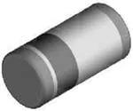
- 封装类型:MELF (DO-213AB)玻璃封装。
- 重量:约135mg。
- 阻燃等级:UL94V-0。
- 湿度敏感等级:按照J-STD-020标准,为MSL 1级。
- 焊接条件:峰值温度不超过260°C。
绝对最大额定值:包括总功耗、稳压电流、结到环境空气的热阻、结到封装的热阻、最大结温、存储温度范围等。
电气特性:详细列出了不同型号稳压二极管的稳压电压范围、测试电流、反向电压、动态电阻、允许的稳压电流和稳压电压的温度系数。
基本特性:提供了稳压二极管的动态电阻与稳压电流的关系图,脉冲热阻与脉冲持续时间的关系图,以及允许的功率耗散与环境温度的关系图。
封装尺寸:提供了MELF DO-213AB (玻璃)封装的尺寸图和引脚识别推荐。
法律声明:文档包含了Vishay对产品规格和数据的免责声明,以及对产品适用性的说明。