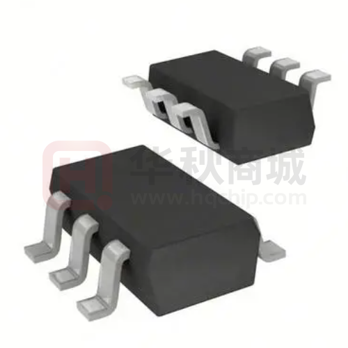
TTP223E-BA6
1 key Touch Pad Detector IC
Outline
z
The TTP223E-BA6 TonTouchTM is a touch pad detector IC which offers 1 touch key. Stable
sensing method can cover diversity conditions. The touching detection IC is designed for
replacing traditional direct button key with diverse pad size. Low power consumption and
wide operating voltage are the contact key features for DC or AC application.
Characteristic
z
Operating voltage 2.0V ~ 5.5V
z
Operating current, @VDD=3V no load
At low power mode typical 2.0uA, maximum 4.0uA
z
The response time max about 220mS at low power mode @VDD=3V
z
Sensitivity can adjust by the capacitance(1~50pF)outside
z
Stable touching detection of human body for replacing traditional direct switch key
z
Provides Low Power mode
z
Provides direct output or toggle output selection by pin option (TOG pin)
z
Q pin is CMOS output can be selected active high or active low by pin option (AHLB pin)
z
After power-on have about 0.5sec stable-time, during the time do not touch the key pad, and
the function is disabled
z
Auto calibration for life
The re-calibration period is about 1 sec within 8 sec after power-on. When key has been
touched within 8 sec or key has not been touched more than 8 sec after power-on, then the
re-calibration period change to 4 sec
Applications
z
Wide consumer products
z
Button key replacement
2016/4/28
Page 1 of 8
Version:1.0
�TTP223E-BA6
Block diagram
I
Sensor &
Reference
detecting circuit
Sensor oscillator
circuit
Timing counter &
function option
control circuit
Output
mode
&
driver
circuit
Q
Touch detecting
circuit
System oscillator
circuit
Key-on & timing
control
Regulator
circuit
TOG
AHLB
Pin Description
Pin NO
Pin Name
Type
1
2
3
Q
VSS
I
O
P
I/O
4
AHLB
I-PL
5
VDD
P
6
TOG
I-PL
Pin Description
CMOS output pin
Negative power supply, ground
Input sensor port
Output Q active high or low selection,
0(Default)=>Active high; 1=>Active low
Positive power supply
Output type option pin,
0(Default)=>Direct output; 1=>Toggle output
Pin Type
z
I
CMOS input only
z
I-PH
CMOS input and pull-high resister
z
O
CMOS push-pull output
z
I-PL
z
I/O
CMOS
z
OD
CMOS input and pull-low resister
Open drain output, have no Diode
protective circuit
z
P
Power/Ground
2016/4/28
I/O
Page 2 of 8
Version:1.0
�TTP223E-BA6
Electrical Characteristics
z
Absolute maximum ratings
Parameter
Symbol
Conditions
Rating
Unit
Operating Temperature
TOP
─
-40~+85
℃
Storage Temperature
TSTG
─
-50~+125
℃
Supply Voltage
VDD
Ta=25°C
VSS-0.3~VSS+5.5
V
VIN
Ta=25°C
VSS-0.3~VDD+0.3
V
ESD
─
5
KV
Input Voltage
Human Body Mode
Note:VSS symbolizes for system ground
z
DC / AC characteristics:(Test condition at room temperature = 25 ℃)
Parameter
Operating Voltage
Symbol
Test Condition
VDD
Min
Typ
Max
Unit
2.0
3
5.5
V
IOPL
VDD=3V, At low power mode
2.0
4.0
uA
IOPF
VDD=3V, At fast mode
5.0
10.0
uA
Input Ports
VIL
Input Low Voltage
0
0.2
VDD
Input Ports
VIH
Input High Voltage
0.8
1.0
VDD
Output Port Sink Current
IOL
VDD=3V, VOL=0.6V
8
mA
Output Port Source Current
IOH
VDD=3V, VOH=2.4V
-4
mA
Input Pin Pull-low Resistor
RPL
25K
ohm
Output Response Time
TR
Operating Current
2016/4/28
VDD=3V
(TOG, AHLB)
VDD=3V、
At fast mode
VDD=3V、
At low power mode
Page 3 of 8
60
mS
220
Version:1.0
�TTP223E-BA6
Function Description
Ⅰ. Sensitivity adjustment
The total loading of electrode size and capacitance of connecting line on PCB can affect the
sensitivity. So the sensitivity adjustment must according to the practical application on PCB. The
TTP223E-BA6 offers some methods for adjusting the sensitivity outside.
1. by the electrode size
Under other conditions are fixed. Using a larger electrode size can increase sensitivity.
Otherwise it can decrease sensitivity. But the electrode size must use in the effective scope.
2. by the panel thickness
Under other conditions are fixed. Using a thinner panel can increase sensitivity. Otherwise it
can decrease sensitivity. But the panel thickness must be below the maximum value.
3. by the value of Cs(please see the down figure)
Under other conditions are fixed. When do not use the Cs to VSS, the sensitivity is most
sensitive. When adding the value of Cs will reduce sensitivity in the useful range
(1≦Cs≦50pF).
VDD
VDD
ELECTRODE
Q
I
Cs
AHLB
TOG
VSS
Ⅱ. Output mode(By TOG、AHLB pin option)
TOG pin:
Direct output or toggle output selection.
AHLB pin:
Output Q active high or active low selection.
Pin Q(CMOS output)option features:
TOG
AHLB
0
0
Direct output, CMOS active high
0
1
Direct output, CMOS active low
1
0
Toggle output, power on state = 0
1
1
Toggle output, power on state = 1
2016/4/28
Pin Q option features
Page 4 of 8
Version:1.0
�TTP223E-BA6
Ⅲ. Low power mode
The TTP223E-BA6 is Low Power mode, it will be saving power. When detecting key touch, it will
switch to Fast mode. Until the key touch is released and will keep a time about 10 sec. Then it
returns to Low Power mode.
Low Power
mode timing
I
Q
Fast mode
timing
Low Power
mode timing
Fast mode
timing
Low Power
mode timing
VDD
VSS
~125ms
~16ms
POSSIBLE KEY TOUCH
KEY RELEASE
(NOT REALLY TOUCH)
~125ms
~16ms
KEY TOUCH
ABOUT 10 SEC
~125ms
KEY RELEASE
VDD
VSS
Low Power Mode
Ⅳ. Option pin
For power saving concern and package bonding option consideration, all the feature option pins
with latch type design and initial states are 0 or 1 as power on. If those pins are forced to VDD
or VSS, the states will be changed to 1 or 0 without any current leakage to conflict the power
saving issue.
2016/4/28
Feature option pins
Initial state by Power on
AHLB
0
TOG
0
Page 5 of 8
Version:1.0
�TTP223E-BA6
Application circuit
VDD
Q
1Q
TOG 6
2 VSS
VDD 5
3I
KEY
AHLB 4
104
Cs
C1
P.S.:
1. On PCB, the length of lines from touch pad to IC pin shorter is better.
And the lines do not parallel and cross with other lines.
2. The power supply must be stable. If the supply voltage drift or shift quickly, maybe causing
sensitivity anomalies or false detections.
3. The material of panel covering on the PCB can not include the metal or the electric element.
The paints on the surfaces are the same.
4. The C1 capacitor must be used between VDD and VSS; and should be routed with very short
tracks to the device’s VDD and VSS pins (TTP223E-BA6).
5. The capacitance Cs can be used to adjust the sensitivity. The value of Cs use smaller, then the
sensitivity will be better. The sensitivity adjustment must according to the practical application on
PCB. The range of Cs value are 1~50pF.
6. The sensitivity adjustment capacitors(Cs)must use smaller temperature coefficient and more
stable capacitors. Such are X7R, NPO for example. So for touch application, recommend to use
NPO capacitor, for reducing that the temperature varies to affect sensitivity.
2016/4/28
Page 6 of 8
Version:1.0
�TTP223E-BA6
Package outline
Package Type: SOT23-6L
2016/4/28
Page 7 of 8
Version:1.0
�TTP223E-BA6
Package configuration
TTP223E-BA6
AHLB
4
VDD
5
6
TOG
Package Type SOT23-6L
223EB
Lot No.
2
3
VSS
I
Q
1
(Latter 4 digit)
Ordering Information
TTP223E-BA6
Package Type
Chip Type
Wafer Type
TTP223E-BA6
No support
No support
REVISE HISTORY
1. 2016/04/28
- Original version:V1.0
2016/4/28
Page 8 of 8
Version:1.0
�
很抱歉,暂时无法提供与“TTP223E-BA6”相匹配的价格&库存,您可以联系我们找货
免费人工找货- 国内价格
- 100+0.45121
- 500+0.44375