XC6202 Series
ETR0302_006
High Voltage Positive Voltage Regulators
■GENERAL DESCRIPTION
The XC6202 series are highly precise, low power consumption, high voltage input, positive voltage regulators manufactured
using CMOS and laser trimming technologies. The XC6202 consists of a current limiter circuit, a driver transistor, a precision
reference voltage and an error correction circuit.
Output voltage is selectable in 0.1V steps from 1.8V ~ 18V. The series are also compatible with low ESR ceramic capacitors
which give added output stability.
Since the current limiter circuit is built-in, the IC is protected against overshoot currents at such times of output shorts etc.
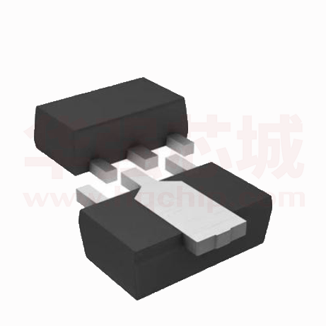
SOT-23, SOT-89, TO-92, SOT-223 and USP-6B packages are available.
■APPLICATIONS
■FEATURES
●Multi-function power supplies
Maximum Output Current
Maximum Operational Voltage
Output Voltage Range
Highly Accurate
Low Power Consumption
Line Regulation
Dropout Voltage
●Digital still cameras / Camcorders
●Reference voltage sources
■TYPICAL APPLICATION CIRCUIT
■TYPICAL PERFORMANCE
CHARACTERISTICS
(12V)
XC6202PC02(12V品)
Ta=25℃
CIN=CL=1μF(ceramic)
12.2
Output Voltage VOUT (V)
●Note PCs / Tablet PCs
: 150mA (within Pd)
: 20V
: 1.8V ~ 18V (0.1V increments)
: ±2%
: 10μA (TYP.)
: 0.01% / V (TYP.)
: 200mV @ 30mA
670mV@100mA
Operational Temperature Range : -40℃ ~ 85℃
Low ESR Capacitor Compatible : Ceramic capacitor
Current Limiter Circuit Built-In
Packages
: SOT-23
SOT-89
TO-92
SOT-223
USP-6B
: EU RoHS Compliant, Pb Free
Environmentally Friendly
12.1
12.0
IOUT= 1mA
=10mA
=30mA
11.9
11.8
13
14
15
16
17
18
19
20
Input Voltage VIN (V)
1/33
�XC6202 Series
■PIN CONFIGURATION
NC
VIN
VSS
NC
NC
VOUT
USP-6B
(BOTTOM VIEW)
*The dissipation pad for the USP-6B package
should be solder-plated in recommended
mount pattern and metal masking so as to
enhance mounting strength and heat release.
If the pad needs to be connected to other pins,
it should be connected to the VSS (No.5) pin.
(SIDE VIEW)
■PIN ASSIGNMENT
PIN NUMBER
SOT-23
SOT-89/TO-92/
SOT-223
USP-6B
1
3
2
-
1
2
3
-
3
5
1
2, 4, 6
2/33
PIN NAME
FUNCTIONS
VOUT
VSS
VIN
NC
Output
Ground
Power Input
No connection
�XC6202
Series
■PRODUCT CLASSIFICATION
●Ordering Information
XC6202P①②③④⑤-⑥(*1)
DESIGNATOR
ITEM
SYMBOL
①②
Output Voltage
18 ~ J0
③
Accuracy
2
MR
④⑤-⑥ (*1)
(*1)
Packages
(Order Unit)
DESCRIPTION
: For the voltage above 10V, see the example
10=A, 11=B 12=C, 13=D, 14=E, 15=F, 16=G, 17=H, 18=J
e.g. VOUT= 3.0V → ①:3, ②:0
VOUT= 12V → ①:C, ②:0
VOUT= 15V → ①:F, ②:0
: ±2%
: SOT-23 (3,000/Reel)
MR-G
: SOT-23 (3,000/Reel)
PR
: SOT-89 (1,000/Reel)
PR-G
: SOT-89 (1,000/Reel)
TH
: TO-92 Taping Type: Paper type (2,000/Tape)
TH-G
: TO-92 Taping Type: Paper type (2,000/Tape)
TB
TB-G
FR
FR-G
DR
: TO-92 Taping Type: Bag (500/Bag)
: TO-92 Taping Type: Bag (500/Bag)
: SOT-223 (1,000/Reel)
: SOT-223 (1,000/Reel)
: USP-6B (3,000/Reel)
DR-G
: USP-6B (3,000/Reel)
The “-G” suffix denotes Halogen and Antimony free as well as being fully EU RoHS compliant.
3/33
�XC6202 Series
■BLOCK DIAGRAM
■ABSOLUTE MAXIMUM RATINGS
Ta = 25℃
PARAMETER
Input Voltage
Output Current
Output Voltage
SOT-23
SOT-89
Power
TO-92
Dissipation
USP-6B
SOT-223
Operating Ambient Temperature
Storage Temperature
SYMBOL
VIN
IOUT
VOUT
* Circuits board mounting: Double-sided board
4/33
Pd
Topr
Tstg
RATINGS
22.0
500
VSS-0.3 ~ VIN+0.3
250
500
300
120
1,200 *
-40~+85
-55~+125
UNITS
V
mA
V
mW
℃
℃
�XC6202
Series
■ELECTRICAL CHARACTERISTICS
XC6202P182
VOUT(T)=1.8V (*1)
PARAMETER
SYMBOL
Output Voltage
VOUT(E) (*2)
Maximum Output Current
IOUTmax
Load Regulation
△VOUT
Input Voltage
Output Voltage
Temperature Characteristics
Vdif1
Vdif2
ISS
△VOUT/
(△VIN・△VOUT)
VIN
△VOUT/
(△Ta・△VOUT)
Short-circuit Current
Ishort
Dropout Voltage(*3)
Supply Current
Line Regulation
XC6202P332
Ta=25℃
CONDITIONS
VIN=2.8V
IOUT=30mA
VIN=2.8V
VOUT≧VOUT(E)×0.9
VIN=2.8V
1mA≦IOUT≦60mA
IOUT=30mA
IOUT=100mA
VIN=2.8V
IOUT=1mA
2.8V≦VIN≦20V
MIN.
TYP.
MAX.
UNITS
CIRCUIT
1.764
1.800
1.836
V
②
60
-
-
mA
②
-
10
80
mV
②
-
340
1000
10
470
1500
24
mV
②
μA
①
-
0.01
0.20
%/V
②
-
-
20
V
-
IOUT=30mA
-40℃≦Ta≦85℃
-
±100
-
ppm/℃
②
VIN=3.8V
-
40
-
mA
②
VOUT(T)=3.3V (*1)
PARAMETER
SYMBOL
Output Voltage
VOUT(E) (*2)
Maximum Output Current
IOUTmax
Load Regulation
△VOUT
Input Voltage
Output Voltage
Temperature Characteristics
Vdif1
Vdif2
ISS
△VOUT/
(△VIN・△VOUT)
VIN
△VOUT/
(△Ta・△VOUT)
Short-circuit Current
Ishort
Dropout Voltage(*3)
Supply Current
Line Regulation
Ta=25℃
CONDITIONS
VIN=4.3V
IOUT=30mA
VIN=4.3V
VOUT≧VOUT(E)×0.9
VIN=4.3V
1mA≦IOUT≦100mA
IOUT=30mA
IOUT=100mA
VIN=4.3V
IOUT=1mA
4.3V≦VIN≦20V
MIN.
TYP.
MAX.
UNITS
CIRCUIT
3.234
3.300
3.366
V
②
150
-
-
mA
②
-
25
90
mV
②
-
200
670
10
280
900
24
mV
②
μA
①
-
0.01
0.20
%/V
②
-
-
20
V
-
IOUT=30mA
-40℃≦Ta≦85℃
-
±100
-
ppm/℃
②
VIN=5.3V
-
40
-
mA
②
5/33
�XC6202 Series
■ELECTRICAL CHARACTERISTICS (Continued)
XC6202P502
VOUT(T)=5.0V (*1)
Ta=25℃
PARAMETER
SYMBOL
Output Voltage
VOUT(E) (*2)
Maximum Output Current
IOUTmax
Load Regulation
△VOUT
Input Voltage
Output Voltage
Temperature Characteristics
Vdif1
Vdif2
ISS
△VOUT/
(△VIN・△VOUT)
VIN
△VOUT/
(△Ta・△VOUT)
Short-circuit Current
Ishort
Dropout Voltage(*3)
Supply Current
Line Regulation
XC6202PC02
MIN.
TYP.
MAX.
UNITS
CIRCUIT
4.900
5.000
5100
V
②
200
-
-
mA
②
-
30
100
mV
②
-
130
440
10
190
550
24
mV
②
μA
①
-
0.01
0.20
%/V
②
-
-
20
V
-
IOUT=30mA
-40℃≦Ta≦85℃
-
±100
-
ppm/℃
②
VIN=7V
-
40
-
mA
②
VOUT(T)=12V (*1)
Ta=25℃
PARAMETER
SYMBOL
Output Voltage
VOUT(E) (*2)
Maximum Output Current
IOUTmax
Load Regulation
△VOUT
Input Voltage
Output Voltage
Temperature Characteristics
Vdif1
Vdif2
ISS
△VOUT/
(△VIN・△VOUT)
VIN
△VOUT/
(△Ta・△VOUT)
Short-circuit Current
Ishort
Dropout Voltage(*3)
Supply Current
Line Regulation
6/33
CONDITIONS
VIN=6V
IOUT=30mA
VIN=6V
VOUT≧VOUT(E)×0.9
VIN=6V
1mA≦IOUT≦100mA
IOUT=30mA
IOUT=100mA
VIN=6V
IOUT=1mA
6V≦VIN≦20V
CONDITIONS
VIN=13V
IOUT=30mA
VIN=13V
VOUT≧VOUT(E)×0.9
VIN=13V
1mA≦IOUT≦100mA
IOUT=30mA
IOUT=100mA
VIN=13V
IOUT=1mA
13V≦VIN≦20V
MIN.
TYP.
MAX.
UNITS
CIRCUIT
11.760
12.000
12.240
V
②
200
-
-
mA
②
-
60
230
mV
②
-
90
290
12
150
380
28
mV
②
μA
①
-
0.01
0.20
%/V
②
-
-
20
V
-
IOUT=30mA
-40℃≦Ta≦85℃
-
±100
-
ppm/℃
②
VIN=14V
-
40
-
mA
②
�XC6202
Series
■ELECTRICAL CHARACTERISTICS (Continued)
XC6202PJ02
VOUT(T)=18V (*1)
Ta=25℃
PARAMETER
SYMBOL
Output Voltage
VOUT(E) (*2)
Maximum Output Current
IOUTmax
Load Regulation
△VOUT
Input Voltage
Output Voltage
Temperature Characteristics
Vdif1
Vdif2
ISS
△VOUT/
(△VIN・△VOUT)
VIN
△VOUT/
(△Ta・△VOUT)
Short-circuit Current
Ishort
Dropout Voltage(*3)
Supply Current
Line Regulation
CONDITIONS
VIN=19V
IOUT=30mA
VIN=19V
VOUT≧VOUT(E)×0.9
VIN=19V
1mA≦IOUT≦100mA
IOUT=30mA
IOUT=100mA
VIN=19V
IOUT=1mA
19V≦VIN≦20V
MIN.
TYP.
MAX.
UNITS
CIRCUIT
17.640
18.000
18.360
V
②
200
-
-
mA
②
-
120
380
mV
②
-
80
280
15
150
380
30
mV
②
μA
①
-
0.01
0.20
%/V
②
-
-
20
V
-
IOUT=30mA
-40℃≦Ta≦85℃
-
±100
-
ppm/℃
②
VIN=20V
-
40
-
mA
②
*1. VOUT(T) = Specified output voltage.
*2. VOUT(E) = Effective output voltage (i.e. the output voltage when “VOUT(T)+1.0V” is provided at the VIN pin while maintaining
certain IOUT value).
*3. Vdif = {VIN1{*5}-VOUT1{*4}}
*4. VOUT1 = A voltage equal to 98% of the output voltage when “VOUT(T) + 1.0V” is input.
*5. VIN1 = The input voltage when VOUT1 is output following a gradual decrease in the input voltage.
■TEST CIRCUITS
CIRCUIT ①
CIRCUIT ②
7/33
�XC6202 Series
■TYPICAL PERFORMANCE CHARACTERISTICS
●XC6202P182
(1) Output Voltage vs. Output Current
XC6202P182(1.8V)
XC6202P182(1.8V)
VIN=2.8V
CIN=CL=1μF(ceramic)
VIN=2.8V
CIN=CL=1μF(ceramic)
-40℃
Ta=25℃
1.8
1.7
2.0
Output Voltage VOUT (V)
Output Voltage VOUT (V)
1.9
85℃
1.6
1.5
0
40
80
120
160
1.5
85℃
-40℃
1.0
0.5
Ta=25℃
0.0
200
0
100
Output Current IOUT (mA)
200
300
400
Output Current IOUT (mA)
(2) Output Voltage vs. Input Voltage
XC6202P182(1.8V)
XC6202P182(1.8V)
Ta=25℃
CIN=CL=1μF(ceramic)
2.00
Output Voltage VOUT (V)
Output Voltage VOUT (V)
2.0
Ta=25℃
CIN=CL=1μF(ceramic)
1.8
1.6
IOUT= 1mA
=10mA
=30mA
1
2
3
IOUT= 1mA
=10mA
=30mA
1.70
(3) Dropout Voltage vs. Output Current
XC6202P182(1.8V)
CIN=CL=1μF(ceramic)
2.0
1.5
85℃
1.0
Ta=25℃
0.5
-40℃
0.0
0
20
40
60
2
4
6
8
10 12 14
Input Voltage VIN (V)
Input Voltge VIN (V)
Dropout Voltage Vdif (V)
1.80
1.60
1.4
80
Output Current IOUT (mA)
8/33
1.90
100
16 18 20
�XC6202
Series
■TYPICAL PERFORMANCE CHARACTERISTICS (Continued)
●XC6202P182 (Continued)
(4) Supply Current vs. Input Voltage
XC6202P182(1.8V)
XC6202P182(1.8V)
14
24
20
Supply Current ISS (μA)
Supply Current ISS (μA)
28
Ta=25℃
16
85℃
12
8
-40℃
4
Ta=25℃
12
85℃
10
8
-40℃
6
0
0
2
4
6
8
2
10 12 14 16 18 20
4
6
XC6202P182(1.8V)
18 20
XC6202P182(1.8V)
VIN=2.8V
CIN=CL=1μF(ceramic)
1.9
1.8
1.7
IOUT= 1mA
=10mA
=30mA
1.5
VIN=2.8V
20
Supply Current ISS (μA)
Output Voltage VOUT (V)
12 14 16
(6) Supply Current vs. Ambient Temperature
(5) Output Voltage vs. Ambient Temperature
1.6
10
Input voltage VIN (V)
Input Voltage VIN (V)
2.0
8
16
12
8
4
0
-40
-20
0
20
40
60
Ambient Temperature Ta ( ℃)
80
100
-40
-20
0
20
40
60
80
100
Ambient Temperature Ta ( ℃)
9/33
�XC6202 Series
■TYPICAL PERFORMANCE CHARACTERISTICS (Continued)
●XC6202P182 (Continued)
(7) Input Transient Response 1
XC6202P182(1.8V)
4
2
0
3
-2
2
-4
Output Voltage
-6
1
0
Input Voltage
3
-2
2
-4
Output Voltage
-6
0
XC6202P182(1.8V)
Iout=30mA、tr=tf=5μs
CL=1μF(ceramic) 、Ta=25℃
1.96
5
1.96
1.92
4
1.92
1.88
Input Voltage
2
1.84
1
1.8
0
Output Voltage
-1
1.76
1.72
XC6202P182(1.8V)
150
120
Output Voltage
1.4
90
1
60
0.6
30mA
Output Current
30
1mA
0.2
0
Time (1ms/div)
10/33
Output Current IOUT (mA)
Output Voltage VOUT (V)
1.8
1.88
Input Voltage
2
1.84
1
1.8
0
Output Voltage
1.76
1.72
Time (0.2ms/div)
(9) Load Transient Response
2.2
3
-1
Time (0.2ms/div)
VIN=2.8V、tr=tf=5μs
CIN=CL=1μF(ceramic) 、Ta=25℃
Input Voltage VIN (V)
3
XC6202P182(1.8V)
Output Voltage VOUT (V)
Input Voltage VIN (V)
4
1
Time (0.1ms/div)
(8) Input Transient Response 2
5
4
0
Time (0.1ms/div)
Iout=1mA、tr=tf=5μs
CL=1μF(ceramic) 、Ta=25℃
5
Output Voltage VOUT (V)
Input Voltage
4
Iout=30mA、tr=5μs
CL=1μF(ceramic) 、Ta=25℃
Output Voltage VOUT (V)
2
5
Input Voltage VIN (V)
Input Voltage VIN (V)
4
Output Voltage VOUT (V)
Iout=1mA、tr=5μs
CL=1μF(ceramic) 、Ta=25℃
XC6202P182(1.8V)
�XC6202
Series
■TYPICAL PERFORMANCE CHARACTERISTICS (Continued)
●XC6202P182 (Continued)
(10) Ripple Rejection Rate
XC6202P182(1.8V)
XC6202P182(1.8V)
VIN=2.8VDC+1Vp-pAC
IOUT=1mA、CL=1μF(ceramic)、Ta=25℃
70
Ripple Rejection Rate PSRR (dB)
Ripple Rejection Rate PSRR (dB)
70
VIN=2.8VDC+1Vp-pAC
IOUT=30mA、CL=1μF(ceramic) 、Ta=25℃
60
50
40
30
20
10
0
0.01
0.1
1
10
Ripple Frequency f (kHz)
60
50
40
30
20
10
0
0.01
0.1
1
10
Ripple Frequency f (kHz)
XC6202P182(1.8V)
VIN=2.8VDC+1Vp-pAC
IOUT=50mA、CL=1μF(ceramic) 、Ta=25℃
Ripple Rejection Rate RR (dB)
70
60
50
40
30
20
10
0
0.01
0.1
1
10
Ripple Frequency f (kHz)
11/33
�XC6202 Series
■TYPICAL PERFORMANCE CHARACTERISTICS (Continued)
●XC6202P332
(1) Output Voltage vs. Output Current
XC6202P332 (3.3V)
XC6202P332 (3.3V)
VIN=4.3V
CIN=CL=1μF(ceramic)
VIN=4.3V
CIN=CL=1μF(ceramic)
4.0
-40℃
3.3
Outout Voltage VOUT (V)
Outout Voltage VOUT (V)
3.4
85℃
3.2
Ta=25℃
3.1
3.0
0
40
80
120
160
3.0
85℃
-40℃
Ta=25℃
2.0
1.0
0.0
200
0
100
200
300
400
Output Current IOUT (mA)
Output Current IOUT (mA)
(2) Output Voltage vs. Input Voltage
XC6202P332 (3.3V)
3.2
3.0
IIOUT= 1mA
=30mA
2.8
2.6
2.8
3.8
3.20
IOUT= 1mA
=30mA
3.10
2
4.8
(3) Dropout Voltage vs. Output Current
XC6202P332 (3.3V)
CIN=CL=1μF( ceramic)
1.6
1.4
85℃
1.2
Ta=25℃
1.0
0.8
0.6
0.4
-40℃
0.2
0.0
0
40
80
120
4
6
8
10 12
14 16
Input Voltage VIN (V)
Input Voltage VIN (V)
Dropout Voltage Vdif (V)
3.30
3.00
2.4
160
Output Current IOUT (mA)
12/33
Ta=25℃
CIN=CL=1μF(ceramic)
3.40
Outout Voltage VOUT (V)
3.4
Outout Voltage VOUT (V)
XC6202P332 (3.3V)
Ta=25℃
CIN=CL=1μF(ceramic)
200
18 20
�XC6202
Series
■TYPICAL PERFORMANCE CHARACTERISTICS (Continued)
●XC6202P332 (Continued)
(4) Supply Current vs. Input Voltage
XC6202P332 (3.3V)
24
24
20
20
Supply Current ISS (μA)
Supply Current ISS (μA)
XC6202P332 (3.3V)
Ta=25℃
16
85℃
12
8
-40℃
4
Ta=25℃
85℃
16
12
8
-40℃
4
0
0
0
2
4
6
8
4
10 12 14 16 18 20
6
8
10
12
14
16
(6) Supply Current vs. Ambient Temperature
(5) Output Voltage vs. Ambient Temperature
XC6202P332 (3.3V)
XC6202P332 (3.3V)
VIN=4.3V
CIN=CL=1μF(ceramic)
3.60
20
3.50
16
3.40
3.30
IOUT= 1mA
=30mA
3.10
Supply Current ISS (μA)
Outout Voltage VOUT (V)
20
Input Voltage VIN (V)
Input Voltage VIN (V)
3.20
18
VIN=4.3V
12
8
4
0
-60 -40 -20
0
20
40
60
Ambient Temperature Ta (℃)
80 100
-60
-40 -20
0
20
40
60
80
100
Ambient Temperature Ta ( ℃)
13/33
�XC6202 Series
■TYPICAL PERFORMANCE CHARACTERISTICS (Continued)
●XC6202P332 (Continued)
(7) Input Transient Response 1
XC6202P332 (3.3V)
IOUT=30mA
CL=1μF(ceramic)、tr=5μs、Ta=25℃
6
4
5
Input Voltage VIN (V)
Input Voltage
2
4
0
3
-2
2
Output Voltage
-4
1
-6
0
Output Voltage VOUT (V)
6
Time (0.1ms/div)
(8) Input Transient Response 2
XC6202P332 (3.3V)
Input Voltage VIN (V)
5
3.7
6
3.6
5
Input Voltage
4
3.5
3
Output Voltage
3.4
2
3.3
1
3.2
(9) Load Transient Response
XC6202P332 (3.3V)
4
Output Voltage
150
120
3
90
2
60
Output Current
1
0
30
30mA
1mA
0
Time (1ms/div)
14/33
Output Current IOUT (mA)
Output Voltage VOUT (V)
5
IOUT=30mA
CL=1μF(ceramic)、tr=tf5μs、Ta=25℃
3.7
3.6
Input Voltage
4
3
3.5
Output Voltage
3.4
2
3.3
1
3.2
Time (0.2ms/div)
Time (0.2ms/div)
VIN=4.3V、tr=tf=5μs
CIN=CL=1μF(ceramic) 、Ta=25℃
Input Voltage VIN (V)
6
Output Voltage VOUT (V)
IOUT=1mA
CL=1μF(ceramic)、tr=tf5us、Ta=25℃
Output Voltage VOUT (V)
XC6202P332 (3.3V)
�XC6202
Series
■TYPICAL PERFORMANCE CHARACTERISTICS (Continued)
●XC6202P332 (Continued)
(10) Ripple Rejection Rate
XC6202P332 (3.3V)
VIN=4.3VDC+1Vp-pAC
IOUT=0.1mA、CL=1μF( c eramic) 、Ta=25℃
80
70
60
50
40
30
20
10
0
0.01
0.1
1
10
VIN=4.3VDC+1Vp-pAC
IOUT=1mA、CL=1μF(ceramic) 、Ta=25℃
80
Ripple Rejection Rate PSRR (dB)
Ripple Rejection Rate PSRR (dB)
XC6202P332 (3.3V)
70
60
50
40
30
20
10
0
100
0.01
Ripple Frequency f (kHz)
60
50
40
30
20
10
0
1
10
100
100
Ripple Frequency f (kHz)
VIN=4.3VDC+1Vp-pAC
IOUT=30mA、CL=1μF(ceramic) 、Ta=25℃
80
Ripple Rejection Rate PSRR (dB)
Ripple Rejection Rate PSRR (dB)
70
0.1
10
XC6202P332 (3.3V)
VIN=4.3VDC+1Vp-pAC
IOUT=10mA、CL=1μF(ceramic) 、Ta=25℃
0.01
1
Ripple Frequency f (kHz)
XC6202P332 (3.3V)
80
0.1
70
60
50
40
30
20
10
0
0.01
0.1
1
10
100
Ripple Frequency f (kHz)
XC6202P332 (3.3V)
VIN=4.3VDC+1Vp-pAC
IOUT=50mA、CL=1μF(ceramic) 、Ta=25℃
Ripple Rejection Rate PSRR (dB)
80
70
60
50
40
30
20
10
0
0.01
0.1
1
10
100
Ripple Frequency f (kHz)
15/33
�XC6202 Series
■TYPICAL PERFORMANCE CHARACTERISTICS (Continued)
●XC6202P502
(1) Output Voltage vs. Output Current
XC6202P502(5V)
XC6202P502(5V)
VIN=6V
CIN=CL=1μF(ceramic)
VIN=6V
CIN=CL=1μF(ceramic)
6
5.1
Output Voltage VOUT (V)
Output Voltage VOUT (V)
-40℃
5.0
85℃
4.9
Ta=25℃
4.8
4.7
4.6
0
40
80
120
160
5
4
85℃
-40℃
3
Ta=25℃
2
1
0
200
0
Output Current IOUT (mA)
100
200
300
400
Output Current IOUT (mA)
(2) Output Voltage vs. Input Voltage
XC6202P502(5V)
XC6202P502(5V)
Ta=25℃
CIN=CL=1μF(ceramic)
Ta=25℃
5.0
Output Voltage VOUT (V)
Output Voltage VOUT (V)
CIN=CL=1μF(ceramic)
5.1
5.2
4.8
IOUT= 1mA
=10mA
=30mA
4.6
4.4
4.2
5.0
4.9
IOUT= 1mA
=10mA
=30mA
4.8
4.7
4.0
4
5
6
6
(3) Dropout Voltage vs. Output Current
XC6202P502(5V)
CIN=CL=1μF(ceramic)
Dropout Voltage Vdif (V)
1.2
85℃
0.8
Ta=25℃
0.6
-40℃
0.4
0.2
0.0
0
40
80
120
160
Output Current IOUT (mA)
16/33
10
12
14
16
Input Voltage VIN (V)
Input Voltage VIN (V)
1.0
8
200
18
20
�XC6202
Series
■TYPICAL PERFORMANCE CHARACTERISTICS (Continued)
●XC6202P502 (Continued)
(4) Supply Current vs. Input Voltage
XC6202P502(5V)
XC6202P502(5V)
14
24
20
Supply Current ISS (μA)
Supply Current ISS (μA)
28
Ta=25℃
16
85℃
12
8
-40℃
4
85℃
12
10
8
Ta=25℃
-40℃
6
0
0
2
4
6
8
4
10 12 14 16 18 20
6
8
10
12
14
16
18
Input Voltage VIN (V)
(5) Output Voltage vs. Ambient Temperature
(6) Supply Current vs. Ambient Temperature
XC6202P502(5V)
XC6202P502(5V)
5.2
20
5.1
16
Supply Current ISS (μA)
Output Voltage VOUT (V)
VIN=6V
CIN=CL=1μF(ceramic)
5.0
4.9
IOUT= 1mA
=10mA
=30mA
4.8
20
Input Voltage VIN (V)
4.7
VIN=6V
12
8
4
0
-40
-20
0
20
40
60
Ambient Temperature Ta ( ℃)
80
100
-40
-20
0
20
40
60
80
100
Ambient Temperature Ta ( ℃)
17/33
�XC6202 Series
■TYPICAL PERFORMANCE CHARACTERISTICS (Continued)
●XC6202P502 (Continued)
(7) Input Transient Response 1
XC6202P502(5V)
Input Voltage
Input Voltage VIN (V)
4
8
7
6
6
2
5
0
4
-2
3
-4
Output Voltage
2
-6
1
-8
0
4
4
-2
3
-4
1
-8
0
8
6.5
7
6.0
Output Voltage
4
5.0
3
4.5
Time (0.2ms/div)
XC6202P502(5V)
150
120
Output Voltage
5
90
4
60
3
30mA
Output Current
30
1mA
2
0
Time (1ms/div)
18/33
Output Current IOUT (mA
Output Voltage VOUT (V)
6
6
Iout=30mA、tr=tf=5μs
CL=1μF(ceramic)、Ta=25℃
7.0
6.5
Input Voltage
5
6.0
5.5
Output Voltage
4
5.0
3
4.5
Time (0.2ms/div)
(9) Load Transient Response
7
2
-6
7.0
5.5
VIN=6V、tr=tf=5μs
CIN=CL=1μF(ceramic),Ta=25℃
Output Voltage
XC6202P502(5V)
Input Voltage VIN (V)
5
6
Time (0.1ms/div)
Output Voltage VOUT (V)
Input Voltage VIN (V)
Input Voltage
6
Input Voltage
0
XC6202P502(5V)
7
7
5
(8) Input Transient Response 2
8
8
2
Time (0.1ms/div)
Iout=1mA、tr=tf=5μs
CL=1μF(ceramic)、Ta=25℃
Iout=30mA、tr=5μs
CL=1μF(ceramic)、Ta=25℃
Output Voltage VOUT (V)
6
8
Input Voltage VIN (V)
8
Output Voltage VOUT (V)
Iout=1mA、tr=5μs
CL=1μF(ceramic)、Ta=25℃
Output Voltage VOUT (V)
XC6202P502(5V)
�XC6202
Series
■TYPICAL PERFORMANCE CHARACTERISTICS (Continued)
●XC6202P502 (Continued)
(10) Ripple Rejection Rate
XC6202P502(5V)
XC6202P502(5V)
VIN=6VDC+1Vp-pAC
IOUT=1mA、CL=1μF(ceramic)
70
Ripple Rejection Rate PSRR (dB)
Ripple Rejection Rate PSRR (dB)
70
VIN=6VDC+1Vp-pAC
IOUT=30mA、CL=1μF(ceramic)
60
50
40
30
20
10
0
0.01
0.1
1
10
Ripple Frequency f (kHz)
60
50
40
30
20
10
0
0.01
0.1
1
10
Ripple Frequency f (kHz)
XC6202P502(5V)
VIN=6VDC+1Vp-pAC
IOUT=50mA、CL=1μF(ceramic)
Ripple Rejection Rate PSRR (dB)
70
60
50
40
30
20
10
0
0.01
0.1
1
10
Ripple Frequency f (kHz)
19/33
�XC6202 Series
■TYPICAL PERFORMANCE CHARACTERISTICS (Continued)
●XC6202PC02
(1) Output Voltage vs. Output Current
XC6202PC02(12V)
XC6202PC02(12V)
VIN=13V
CIN=CL=1μF(ceramic)
VIN=13V
12.5
Output Voltage VOUT (V)
Output Voltage VOUT (V)
16
CIN=CL=1μF( ceramic)
13.0
-40℃
12.0
85℃
11.5
Ta=25℃
11.0
10.5
10.0
12
85℃
-40℃
8
4
Ta=25℃
0
0
40
80
120
160
200
0
100
200
300
400
Output Current IOUT (mA)
Output Current IOUT (mA)
(2) Output Voltage vs. Input Voltage
XC6202PC02(12V)
12.2
Ta=25℃
12.0
11.8
11.6
IOUT= 1mA
=10mA
=30mA
11.4
11.2
11.0
12
13
Input Voltage VIN (V)
12.0
IOUT= 1mA
=10mA
=30mA
11.9
XC6202PC02(12V)
CIN=CL=1μF( ceramic)
1.2
1.0
85℃
0.8
Ta=25℃
0.6
0.4
-40℃
0.2
0.0
0
40
80
120
13
14
15
16
17
18
Input Voltage VIN (V)
(3) Dropout Voltage vs. Output Current
Dropout Voltage Vdif (V)
12.1
11.8
11
160
Output Current IOUT (mA)
20/33
CIN=CL=1μF(ceramic)
12.2
Output Voltage VOUT (V)
Output Voltage VOUT (V)
XC6202PC02(12V)
Ta=25℃
CIN=CL=1μF( ceramic)
200
19
20
�XC6202
Series
■TYPICAL PERFORMANCE CHARACTERISTICS (Continued)
●XC6202PC02 (Continued)
(4) Supply Current vs. Input Voltage
XC6202PC02(12V)
24
50
45
40
35
30
25
20
15
10
5
0
Supply Current ISS (μA)
Supply Current ISS (μA)
XC6202PC02(12V)
85℃
Ta=25℃
-40℃
20
Ta=25℃
16
85℃
12
8
-40℃
4
0
0
2
4
6
8
13
10 12 14 16 18 20
14
(5) Output Voltage vs. Ambient Temperature
17
18
19
20
(6) Supply Current vs. Ambient Temperature
XC6202PC02(12V)
XC6202PC02(12V)
VIN=13V
CIN=CL=1μF(Ceramic)
12.2
20
12.1
16
Supply Current ISS (μA)
Output Voltage VOUT (V)
16
Input Voltage VIN (V)
Input Voltage VIN (V)
12.0
11.9
IOUT= 1mA
=10mA
=30mA
11.8
15
11.7
VIN=13V
12
8
4
0
-40
-20
0
20
40
60
80
Ambient Temperature Ta ( ℃)
100
-40
-20
0
20
40
60
80
100
Ambient Temperature Ta ( ℃)
21/33
�XC6202 Series
■TYPICAL PERFORMANCE CHARACTERISTICS (Continued)
●XC6202PC02 (Continued)
(7) Input Transient Response 1
Input Voltage
15
16
10
5
12
0
8
-5
4
Output Voltage
-10
Input Voltage VIN (V)
10
20
Output Voltage VOUT (V)
Iout=1mA、tr=5μs
CL=1μF(ceramic)、Ta=25℃
15
Input Voltage VIN (V)
XC6202PC02(12V)
0
Iout=30mA、tr=5μs
CL=1μF(ceramic)、Ta=25℃
Input Voltage
20
16
5
12
0
8
-5
Output Voltage
-10
Time
(0.4ms/div)
Time
(0.4ms/div)
4
Output Voltage VOUT (V)
XC6202PC02(12V)
0
Time
Time (0.4ms/div)
(0.4ms/div)
(8) Input Transient Response 2
XC6202PC02(12V)
13
Input Voltage
15
12.4
14
12.3
12
12.2
11
12.1
10
12.0
Output Voltage
9
XC6202PC02(12V)
Output Voltage VOUT (V)
150
120
Output Voltage
90
30mA
Output Current
9
60
30
1mA
8
0
Time (1ms/div)
22/33
Output Current IOUT (mA
VIN=13V、tr=tf=5us
CIN=CL=1μF(ceramic),Ta=25℃
10
Input Voltage
12.3
12
12.2
11
12.1
10
12.0
11.9
Time (1ms/div)
(9) Load Transient Response
11
12.4
9
Time (1ms/div)
12
12.5
Output Voltage
11.9
13
13
CL=1μF(ceramic)、Ta=25℃
Output Voltage VOUT (V)
Input Voltage VIN (V)
14
12.5
Input Voltage VIN (V)
15
Iout=30mA、tr=tf=5μs
Output Voltage VOUT (V)
Iout=1mA、tr=tf=5μs
CL=1μF(ceramic)、Ta=25℃
XC6202PC02(12V)
�XC6202
Series
■TYPICAL PERFORMANCE CHARACTERISTICS (Continued)
●XC6202PC02 (Continued)
(10) Ripple Rejection Rate
XC6202PC02(12V)
XC6202PC02(12V)
VIN=13VDC+1Vp-pAC
IOUT=1mA、CL=1μF( ceramic) 、Ta=25℃
70
Ripple Rejection Rate PSRR (dB)
70
Ripple Rejection Rate PSRR (dB)
VIN=13VDC+1Vp-pAC
IOUT=30mA、CL=1μF(ceramic) 、Ta=25℃
60
50
40
30
20
10
0
0.01
0.1
1
10
Ripple Frequency f (kHz)
60
50
40
30
20
10
0
0.01
0.1
1
10
Ripple Frequency f (kHz)
XC6202PC02(12V)
VIN=13VDC+1Vp-pAC
IOUT=50mA、CL=1μF(ceramic) 、Ta=25℃
Ripple Rejection Rate PSRR (dB)
70
60
50
40
30
20
10
0
0.01
0.1
1
10
Ripple Frequency f (kHz)
23/33
�XC6202 Series
■TYPICAL PERFORMANCE CHARACTERISTICS (Continued)
●XC6202PJ02
(1) Output Voltage vs. Output Current
XC6202PJ02(18V)
XC6202PJ02(18V)
VIN=19V
CIN=CL=1μF(ceramic)
VIN=19V
CIN=CL=1μF(ceramic)
20
18.5
Output Voltage VOUT (V)
Output Voltage VOUT (V)
19.0
-40℃
18.0
85℃
17.5
Ta=25℃
17.0
16.5
16.0
0
40
80
120
160
15
85℃
10
Ta=25℃
5
0
200
0
100
(2) Output Voltage vs. Input Voltage
400
CIN=CL=1μF(ceramic)
18.2
1.2
18.0
1.0
Dropout Voltage Vdif (V)
Output Voltage VOUT (V)
Ta=25℃
CIN=CL=1μF(ceramic)
17.8
17.6
IOUT= 1mA
=10mA
=30mA
0.8
Ta=25℃
0.6
85℃
0.4
0.2
-40℃
0.0
17.0
17
18
19
20
0
40
80
120
160
200
Output Curren IOUT (mA)
Input Voltage VIN (V)
(5) Output Voltage vs. Ambient Temperature
(4) Supply Current vs. Input Voltage
XC6202PJ02(18V)
XC6202PJ02(18V)
VIN=19V
CIN=CL=1μF(ceramic)
70
18.2
60
50
Ta= 85℃
25℃
40
30
20
-40℃
10
Output Voltage VOUT (V)
Supply Current ISS (μA)
300
(3) Dropout Voltage vs. Output Current
XC6202PJ02(18V)
XC6202PJ02(18V)
17.2
200
Output Current IOUT (mA)
Output Curren IOUT (mA)
17.4
-40℃
18.1
18.0
17.9
IOUT= 1mA
=10mA
=30mA
17.8
0
0
2
4
6
8
10 12 14 16 18 20
Input Voltage VIN (V)
17.7
-40
-20
0
20
40
60
80
Ambient Temperature Ta ( ℃)
24/33
100
�XC6202
Series
■TYPICAL PERFORMANCE CHARACTERISTICS (Continued)
●XC6202PJ02 (Continued)
(6) Supply Current vs. Ambient Temperature
XC6202PJ02(18V)
VIN=19V
Supply Current ISS (μA)
20
16
12
8
4
0
-40
-20
0
20
40
60
80
100
Ambient Temperature Ta ( ℃)
(7) Input Transient Response 1
XC6202PJ02(18V)
Iout=1mA、tr=5μs
CL=1μF(ceramic)、Ta=25℃
Input Voltage
10
30
25
20
20
0
15
-10
10
-20
Output Voltage
-30
5
Input Voltage VIN (V)
Input Voltage VIN (V)
20
30
Output Voltage VOUT (V)
30
30
25
Input Voltage
10
20
0
15
-10
10
-20
0
Iout=30mA、tr=5μs
CL=1μF(ceramic) 、Ta=25℃
Output Voltage
-30
Time (0.4ms/div)
5
Output Voltage VOUT (V)
XC6202PJ02(18V)
0
Time (0.4ms/div)
(8) Input Transient Response 2
19
Input Voltage
18
17
21
18.4
20
18.3
18.2
Output Voltage
16
18.1
18.0
15
17.9
Time (1ms/div)
Input Voltage VIN (V)
Input Voltage VIN (V)
20
18.5
Output Voltage VOUT (V)
21
Iout=1mA、t=tfr=5μs
CL=1μF(ceramic) 、Ta=25℃
XC6202PJ02(18V)
19
Iout=30mA、tr=tf=5μs
CL=1μF(ceramic) 、Ta=25℃
18.4
Input Voltage
18
17
18.5
18.3
18.2
Output Voltage
18.1
16
18.0
15
17.9
Output Voltage VOUT (V)
XC6202PJ02(18V)
Time (1ms/div)
25/33
�XC6202 Series
■TYPICAL PERFORMANCE CHARACTERISTICS (Continued)
●XC6202PJ02 (Continued)
(9) Load Transient Response
XC6202PJ02(18V)
Output Voltage VOUT (V)
19
18
150
120
Output Voltage
17
90
16
60
Output Current
15
30
30mA
1mA
14
Output Current IOUT (mA
VIN=19V、tr=tf=5us
CIN=CL=1μF(ceramic) 、Ta=25℃
0
Time (1ms/div)
(10) Ripple Rejection Rate
XC6202PJ02(18V)
60
50
40
30
20
10
0
0.01
0.1
1
10
Ripple Frequency f (kHz)
VIN=19VDC+1Vp-pAC
IOUT=50mA、CL=1μF(ceramic)、Ta=25℃
Ripple Rejection Rate PSRR (dB)
60
50
40
30
20
10
0
0.01
0.1
1
Ripple Frequency f (kHz)
26/33
60
50
40
30
20
10
0
0.01
0.1
1
Ripple Frequency f (kHz)
XC6202PJ02(18V)
70
VIN=19VDC+1Vp-pAC
IOUT=30mA、CL=1μF(ceramic)、Ta=25℃
70
Ripple Rejection Rate PSRR (dB)
70
Ripple Rejection Rate PSRR (dB)
XC6202PJ02(18V)
VIN=19VDC+1Vp-pAC
IOUT=1mA、CL=1μF(ceramic)、Ta=25℃
10
10
�XC6202
Series
■PACKAGING INFORMATION
●SOT-23
Unit : mm
●SOT-89
Unit : mm
27/33
�XC6202 Series
■PACKAGING INFORMATION (Continued)
●TO-92
Paper type
Bag
●SOT-223
Unit : mm
28/33
�XC6202
Series
■PACKAGING INFORMATION (Continued)
●USP-6B
Unit : mm
●USP-6B Recommended Pattern Layout
●USP-6B Recommended Metal Mask Design
29/33
�XC6202 Series
■MARKING RULE
●SOT-23, SOT-89, SOT-223
②
③ ④
1
④
①
①
①
②
③
④
③
②
3
2
1
2
3
1
2
3
① represents product series
MARK
PRODUCT SERIES
2
XC6202Pxxxxx
② represents output voltage range
MARK
VOLTAGE (V)
PRODUCT SERIES
4
5
6
7
8
9
0.1 ~ 3.0
3.1 ~ 6.0
6.1 ~ 9.0
9.1 ~ 12.0
12.1 ~ 15.0
15.1 ~ 18.0
XC6202Pxxxxx
③ represents output voltage
MARK
VOLTAGE (V)
MARK
VOLTAGE (V)
0
-
3.1
6.1
9.1
12.1
15.1
F
-
4.6
7.6
10.6
13.6
16.6
1
-
3.2
6.2
9.2
12.2
15.2
H
-
4.7
7.7
10.7
13.7
16.7
2
-
3.3
6.3
9.3
12.3
15.3
K
1.8
4.8
7.8
10.8
13.8
16.8
3
-
3.4
6.4
9.4
12.4
15.4
L
1.9
4.9
7.9
10.9
13.9
16.9
4
-
3.5
6.5
9.5
12.5
15.5
M
2.0
5.0
8.0
11.0
14.0
17.0
5
-
3.6
6.6
9.6
12.6
15.6
N
2.1
5.1
8.1
11.1
14.1
17.1
6
-
3.7
6.7
9.7
12.7
15.7
P
2.2
5.2
8.2
11.2
14.2
17.2
7
-
3.8
6.8
9.8
12.8
15.8
R
2.3
5.3
8.3
11.3
14.3
17.3
8
-
3.9
6.9
9.9
12.9
15.9
S
2.4
5.4
8.4
11.4
14.4
17.4
9
-
4.0
7.0
10.0
13.0
16.0
T
2.5
5.5
8.5
11.5
14.5
17.5
A
-
4.1
7.1
10.1
13.1
16.1
U
2.6
5.6
8.6
11.6
14.6
17.6
B
-
4.2
7.2
10.2
13.2
16.2
V
2.7
5.7
8.7
11.7
14.7
17.7
C
-
4.3
7.3
10.3
13.3
16.3
X
2.8
5.8
8.8
11.8
14.8
17.8
D
-
4.4
7.4
10.4
13.4
16.4
Y
2.9
5.9
8.9
11.9
14.9
17.9
E
-
4.5
7.5
10.5
13.5
16.5
Z
3.0
6.0
9.0
12.0
15.0
18.0
④ represents production lot number
0 to 9, A to Z reversed character 0 to 9, A to Z repeated. (G, I, J, O, Q, W excluded)
30/33
�XC6202
Series
■MARKING RULE(Continued)
●TO-92
TO-92
(SIDE VIEW)
① represents type of regulator
MARK
PRODUCT SERIES
P
XC6202Pxxxxx
② represents integer of the output voltage
MARK
VOLTAGE (V)
PRODUCT SERIES
MARK
VOLTAGE (V)
PRODUCT SERIES
1
1.x
XC6202P1xxxx
A
10.x
XC6202PAxxxx
2
3
4
2.x
3.x
4.x
XC6202P2xxxx
XC6202P3xxxx
XC6202P4xxxx
B
C
D
11.x
12.x
13.x
XC6202PBxxxx
XC6202PCxxxx
XC6202PDxxxx
5
5.x
XC6202P5xxxx
E
14.x
XC6202PExxxx
6
6.x
XC6202P6xxxx
F
15.x
XC6202PFxxxx
7
7.x
XC6202P7xxxx
G
16.x
XC6202PGxxxx
8
8.x
XC6202P8xxxx
H
17.x
XC6202PHxxxx
9
9.x
XC6202P9xxxx
J
18.x
XC6202PJxxxx
③ represents decimal number of output voltage
MARK
VOLTAGE (V)
PRODUCT SERIES
3
0
x.3
x.0
XC6202Px3xxx
XC6202Px0xxx
④ represents detect voltage accuracy
MARK
DETECT VOLTAGE ACCURACY
PRODUCT SERIES
2
Within ±2%
XC6202Pxx2xx
1
Within ±1%
XC6202Pxx1xx
⑤ represents a least significant digit of production year
MARK
3
4
PRODUCTION YEAR
2003
2004
⑥ represents production lot number
0 to 9, A to Z repeated (G, I, J, O, Q, W excluded)
Note: No character inversion used.
31/33
�XC6202 Series
■MARKING RULE (Continued)
●USP-6B
①② represents product series
MARK
①
②
0
2
PRODUCT SERIES
XC6202PxxxDx
③ represents type of regulator
MARK
PRODUCT SERIES
P
XC6202Pxxxxx
④ represents integer of the output voltage
MARK
VOLTAGE (V)
PRODUCT SERIES
MARK
VOLTAGE (V)
1
1.x
2
2.x
3
4
PRODUCT SERIES
XC6202P1xxDx
A
10.x
XC6202PAxxDx
XC6202P2xxDx
B
11.x
XC6202PBxxDx
3.x
XC6202P3xxDx
C
12.x
XC6202PCxxDx
4.x
XC6202P4xxDx
D
13.x
XC6202PDxxDx
5
5.x
XC6202P5xxDx
E
14.x
XC6202PExxDx
6
6.x
XC6202P6xxDx
F
15.x
XC6202PFxxDx
7
7.x
XC6202P7xxDx
G
16.x
XC6202PGxxDx
8
8.x
XC6202P8xxDx
H
17.x
XC6202PHxxDx
9
9.x
XC6202P9xxDx
J
18.x
XC6202PJxxDx
⑤ represents decimal number of output voltage
MARK
VOLTAGE (V)
PRODUCT SERIES
3
0
X.3
X.0
XC6202Px3xDx
XC6202Px0xDx
⑥ represents production lot number
0 to 9, A to Z repeated (G, I, J, O, Q, W excluded)
Note: No character inversion used.
32/33
�XC6202
Series
1. The products and product specifications contained herein are subject to change without
notice to improve performance characteristics.
Consult us, or our representatives
before use, to confirm that the information in this datasheet is up to date.
2. We assume no responsibility for any infringement of patents, patent rights, or other
rights arising from the use of any information and circuitry in this datasheet..
3. Please ensure suitable shipping controls (including fail-safe designs and aging
protection) are in force for equipment employing products listed in this datasheet.
4. The products in this datasheet are not developed, designed, or approved for use with
such equipment whose failure of malfunction can be reasonably expected to directly
endanger the life of, or cause significant injury to, the user.
(e.g. Atomic energy; aerospace; transport; combustion and associated safety
equipment thereof.)
5. Please use the products listed in this datasheet within the specified ranges.
Should you wish to use the products under conditions exceeding the specifications,
please consult us or our representatives.
6. We assume no responsibility for damage or loss due to abnormal use.
7. All rights reserved. No part of this datasheet may be copied or reproduced without the
prior permission of TOREX SEMICONDUCTOR LTD.
33/33
�