XC62FJ Series
ETR03086-001
10V Input, 200mA Low Consumption Current Regulator
■GENERAL DESCRIPTION
The XC62FJ series is a highly precise, low power consumption, positive voltage regulator manufactured with CMOS and
laser trimming technologies.
The series provides large currents with a significantly small dropout voltage.
The XC62FJ consists of a current limiter circuit, a driver transistor, a precision reference voltage and an error amplifier.
The output voltage is selectable in 0.1V steps between 1.7V ~ 6.0V.
■APPLICATIONS
■FEATURES
● Smart meter
Maximum Output Current
:
● Walky-talky
Dropout Voltage
:
● Blood pressure manometer
Operating Voltage Range
Output Voltage Range
:
:
Consumption Current
External Capacitor
Operating Ambient Temperature
Package
Environmentally Friendly
:
:
:
:
:
■TYPICAL APPLICATION CIRCUIT
■TYPICAL PERFORMANCE
CHARACTERISTICS
●Consumption Current vs. Input Voltage
XC62FJ3302PR-G
3.0
Consumption Current: ISS(uA)
● Applications with 2Li-ion batteries
200mA
160mV@IOUT=100mA
(VOUT=5.0V)
1.8V~10V
1.7V~6.0V (±2.0%)
0.1V increments
2.0μA (TYP.)
Ceramic Capacitor
-40℃~+85℃
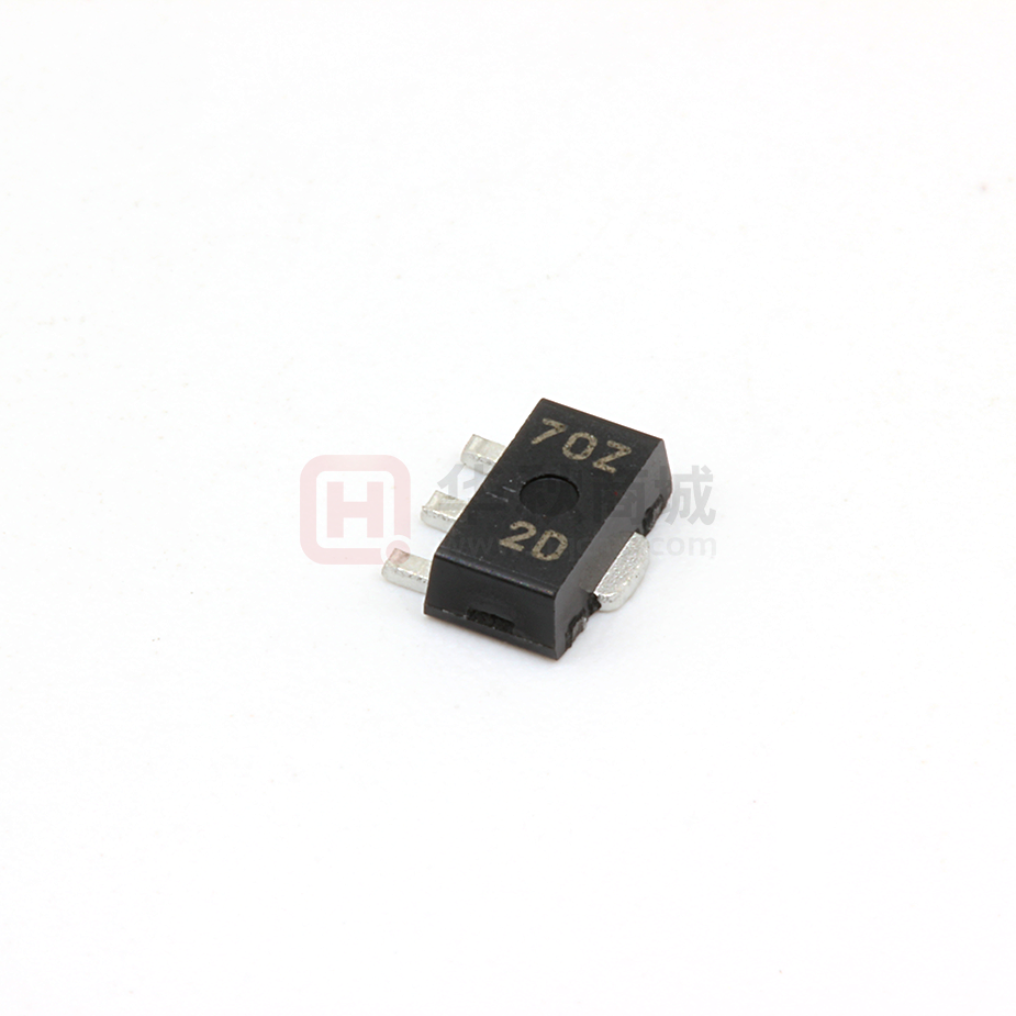
SOT-89
EU RoHS Compliant, Pb Free
2.5
2.0
1.5
Ta=-40℃
1.0
Ta=25℃
0.5
Ta=85℃
0.0
0
2
4
6
8
10
Input Voltage: VIN(V)
1/16
�XC62FJ Series
■BLOCK DIAGRAM
XC62FJ Series
* Diodes inside the circuits are ESD protection diodes and parasitic diodes.
■PIN CONFIGURATION
1
2
3
VSS
VIN
VOUT
SOT-89
(TOP VIEW)
■PIN ASSIGNMENT
PIN NUMBER
PIN NAME
FUNCTION
1
VSS
Ground
2
VIN
Power Supply Input
3
VOUT
Output
SOT-89
2/16
�XC62FJ
Series
■PRODUCT CLASSIFICATION
●Ordering Information
XC62FJ①②③④⑤⑥-⑦
DESIGNATOR
DESCRIPTION
SYMBOL
①②
Output Voltage
17~60
③④
Output Voltage Accuracy
02
⑤⑥-⑦(*1)
Package (Order Unit)
PR-G
(*1)
DESCRIPTION
e.g. 30: 3.0V, 50: 5.0V
±2.0%
SOT-89 (1,000/Reel)
The “-G” suffix denotes Halogen and Antimony free as well as being fully EU RoHS compliant.
■ABSOLUTE MAXIMUM RATINGS
PARAMETER
SYMBOL
RATINGS
Input Voltage
VIN
- 0.3 ~ + 12.0
IOUT
500 (*1)
Output Current
Output Voltage
Power Dissipation
(*1)
VOUT
SOT-89
Pd
- 0.3 ~ VIN + 0.3 or +12.0
1000 (PCB
mounted) (*3)
Ta=25℃
UNITS
V
mA
(*2)
V
mW
Operating Ambient Temperature
Topr
-40~+85
℃
Storage Temperature
Tstg
-55~+125
℃
All voltages are described based on VSS.
(*1)
IOUT≦Pd/ (VIN-VOUT)
(*2)
The maximum value should be either VIN+0.3 or +12.0 in the lowest
(*3)
The power dissipation figure shown is PCB mounted. Please refer to page 14 for details.
3/16
�XC62FJ Series
■ELECTRICAL CHARACTERISTICS
Ta=25℃
PARAMETER
SYMBOL
Output Voltage
VOUT(E) (*2)
Maximum Output Current
IOUTMAX
Load Regulation
∆VOUT
Dropout Voltage1
Vdif1 (*3)
Dropout Voltage2
(*3)
Consumption current
Line Regulation
Input Voltage(*6)
Output Voltage
Temperature
(*1)
(*2)
(*3)
(*4)
(*5)
(*6)
Vdif2
ISS
∆VOUT/
(∆VIN・VOUT)
VIN
∆VOUT/
CONDITIONS
VIN=VOUT(T)(*1)+1.0V、IOUT={C1(*6)}mA
VIN=VOUT(T)+1.0V
VOUT(E)≧VOUT(T)×0.9
VIN=VOUT(T)+1.0V
MIN
TYP
MAX
UNIT
CIRCUIT
E-1 (*5)
VOUT(T)
E-1 (*5)
V
②
E-2 (*5)
-
-
mA
②
-
E-3 (*5)
mV
②
-
E-4 (*5)
mV
②
}mA
-
(*5)
mV
②
VIN=VOUT(T)+1.0V
-
2.0
E-6 (*5)
μA
①
-
0.2
0.3
%/V
②
1.8
-
10
V
-
1mA≦IOUT≦{C2 (*6)}mA
IOUT={C3 (*6)}mA
IOUT={C4
(*6)
VOUT(T)+1.0V≦VIN≦10.0V
IOUT={C5 (*6)}mA
IOUT={C1 (*6)}mA
E-5
±100
ppm/℃
-40℃≦Topr≦85℃
Characteristics
VOUT(T) is Nominal output voltage
VOUT(E) is Effective output voltage
(i.e. the output voltage when “(VOUT(T) + 1.0V)” is provided at the VIN pin while maintaining a certain IOUT value.)
Vdif={VIN1-VOUT1}
VIN1 is the input voltage when VOUT1 appears at the VOUT pin while input voltage is gradually decreased.
VOUT1 is the voltage equal to 98% of the normal output voltage when amply stabilized VOUT(T) +1.0V is input at the VIN pin.
Over 1.8V input voltage (Minimum operation voltage) is required when the VOUT is lower than 1.8V.
Refer to the VOLTAGE CHART
Refer to the VOLTAGE CONDITIONS CHART
4/16
(∆Topr・VOUT)
②
�XC62FJ
Series
■ELECTRICAL CHARACTERISTICS
VOLTAGE CHART
SYMBOL
E-1
NOMINAL
OUTPUT
OUTPUT
VOLTAGE
VOLTAGE
VOUT(T)
E-2
E-3
MAXIMUM
OUTPUT
CURRENT
E-4
E-5
E-6
LOAD
DROPOUT
DROPOUT
CONSUMPTION
REGULATION
VOLTAGE1
VOLTAGE2
CURRENT
(V)
(mA)
(mV)
(mV)
(mV)
(μA)
VOUT(E)
IOUTMAX
∆VOUT
Vdif1
Vdif2
ISS
MIN.
MAX.
MIN.
TYP.
MAX.
TYP.
MAX.
TYP.
MAX.
MAX.
1.7
1.666
1.734
80
10
30
200
370
450
710
5.0
1.8
1.764
1.836
80
10
30
200
370
450
710
5.0
1.9
1.862
1.938
80
10
30
200
370
450
710
5.0
2.0
1.960
2.040
100
15
40
200
370
450
710
5.0
2.1
2.058
2.142
100
15
40
200
370
450
710
5.0
2.2
2.156
2.244
100
15
40
200
370
450
710
5.0
2.3
2.254
2.346
100
15
40
200
370
450
710
5.0
2.4
2.352
2.448
100
15
40
200
370
450
710
5.0
2.5
2.450
2.550
100
15
40
200
370
450
710
5.0
2.6
2.548
2.652
100
15
40
200
370
450
710
5.0
2.7
2.646
2.754
100
15
40
200
370
450
710
5.0
2.8
2.744
2.856
100
15
40
200
370
450
710
5.0
2.9
2.842
2.958
100
15
40
200
370
450
710
5.0
3.0
2.940
3.060
150
20
50
200
360
450
700
5.0
3.1
3.038
3.162
150
20
50
200
360
450
700
5.0
3.2
3.136
3.264
150
20
50
200
360
450
700
5.0
3.3
3.234
3.366
150
20
50
200
360
450
700
5.0
3.4
3.332
3.468
150
20
50
200
360
450
700
5.0
3.5
3.430
3.570
150
20
50
200
360
450
700
5.0
3.6
3.528
3.672
150
20
50
200
360
450
700
5.0
3.7
3.626
3.774
150
20
50
200
360
450
700
5.0
3.8
3.724
3.876
150
20
50
200
360
450
700
5.0
3.9
3.822
3.978
150
20
50
200
360
450
700
5.0
4.0
3.920
4.080
180
25
60
180
350
420
630
6.0
4.1
4.018
4.182
180
25
60
180
350
420
630
6.0
4.2
4.116
4.284
180
25
60
180
350
420
630
6.0
4.3
4.214
4.386
180
25
60
180
350
420
630
6.0
4.4
4.312
4.488
180
25
60
180
350
420
630
6.0
4.5
4.410
4.590
180
25
60
180
350
420
630
6.0
4.6
4.508
4.692
180
25
60
180
350
420
630
6.0
4.7
4.606
4.794
180
25
60
180
350
420
630
6.0
4.8
4.704
4.896
180
25
60
180
350
420
630
6.0
4.9
4.802
4.998
180
25
60
180
350
420
630
6.0
5.0
4.900
5.100
200
30
70
160
340
400
600
6.0
5.1
4.998
5.202
200
30
70
160
340
400
600
6.0
5.2
5.096
5.304
200
30
70
160
340
400
600
6.0
5.3
5.194
5.406
200
30
70
160
340
400
600
6.0
5.4
5.292
5.508
200
30
70
160
340
400
600
6.0
5.5
5.390
5.610
200
30
70
160
340
400
600
6.0
5.6
5.488
5.712
200
30
70
160
340
400
600
6.0
5.7
5.586
5.814
200
30
70
160
340
400
600
6.0
5.8
5.684
5.916
200
30
70
160
340
400
600
6.0
5.9
5.782
6.018
200
30
70
160
340
400
600
6.0
6.0
5.880
6.120
200
30
70
150
330
400
600
6.0
5/16
�XC62FJ Series
■ELECTRICAL CHARACTERISTICS (Continued)
VOLTAGE CONDITIONS CHART
C1
NOMINAL
C3
C4
C5
OUTPUT
LOAD
DROPOUT
DROPOUT
LINE
VOLTAGE
REGULATION
VOLTAGE1
VOLTAGE2
REGULATION
VOUT(T)
IOUT (mA)
IOUT (mA)
IOUT (mA)
IOUT (mA)
IOUT (mA)
1.7
40
40
40
80
40
1.8
40
40
40
80
40
1.9
40
40
40
80
40
2.0
40
60
60
120
40
2.1
40
60
60
120
40
2.2
40
60
60
120
40
2.3
40
60
60
120
40
2.4
40
60
60
120
40
2.5
40
60
60
120
40
2.6
40
60
60
120
40
2.7
40
60
60
120
40
2.8
40
60
60
120
40
2.9
40
60
60
120
40
3.0
40
80
80
160
40
3.1
40
80
80
160
40
3.2
40
80
80
160
40
3.3
40
80
80
160
40
3.4
40
80
80
160
40
3.5
40
80
80
160
40
3.6
40
80
80
160
40
3.7
40
80
80
160
40
3.8
40
80
80
160
40
3.9
40
80
80
160
40
4.0
40
100
100
200
40
4.1
40
100
100
200
40
4.2
40
100
100
200
40
4.3
40
100
100
200
40
4.4
40
100
100
200
40
4.5
40
100
100
200
40
4.6
40
100
100
200
40
4.7
40
100
100
200
40
4.8
40
100
100
200
40
4.9
40
100
100
200
40
5.0
40
100
100
200
40
5.1
40
100
100
200
40
5.2
40
100
100
200
40
5.3
40
100
100
200
40
5.4
40
100
100
200
40
5.5
40
100
100
200
40
5.6
40
100
100
200
40
5.7
40
100
100
200
40
5.8
40
100
100
200
40
5.9
40
100
100
200
40
6.0
40
100
100
200
40
OUTPUT VOLTAGE
6/16
C2
�XC62FJ
Series
■TEST CIRCUITS
CIRCUIT①
CIRCUIT②
■OPERATIONAL EXPLANATION
The XC62FJ series needs an output capacitor CL for phase compensation.
In order to ensure the stable phase compensation, please place an
output capacitor of 1.0μF or bigger at the VOUT pin and VSS pin as close as possible.
For a stable power input, please connect an input capacitor
(CIN) of 1.0μF between the input pin (VIN) and the ground pin (VSS).
7/16
�XC62FJ Series
■NOTES ON USE
1. For temporary, transitional voltage drop or voltage rising phenomenon, the IC is liable to malfunction should the ratings be
exceeded.
2. Where wiring impedance is high, operations may become unstable due to noise and/or phase lag depending on output current.
3. An oscillation may occur by the impedance between a power supply and the input of the IC. Where the impedance is 10Ωor
more, please use an input capacitor (CIN) of at least 1μF. In case of high output current, operation can be stabilized by
increasing the input capacitor value. Also an oscillation may occur if the input capacitor value is smaller than the input
impedance when the output capacitance (CL) is large. In such cases, operations can be stabilized by either increasing the input
capacitor value or reducing the output capacitor value.
4. Torex places an importance on improving our products and their reliability.
We request that users incorporate fail-safe designs and post-aging prevention treatment when using Torex products in their
systems.
8/16
�XC62FJ
Series
■TYPICAL PERFORMANCE CHARACTERISTICS
(1)Output Voltage vs. Output Current
XC62FJ3302PR-G
V IN=4.3V CIN=CL=1.0uF(ceramic)
Output Voltage: VOUT(V)
3.5
3.0
2.5
2.0
1.5
Ta=-40℃
1.0
Ta=25℃
0.5
Ta=85℃
0.0
0
100
200
300
400
500
Output Current: IOUT(mA)
(2) Output Voltage vs. Input Voltage
XC62FJ3302PR-G
XC62FJ3302PR-G
3.3
3.1
IOUT=0mA
2.9
IOUT=1mA
2.7
3.5
Output Voltage: VOUT(V)
Output Voltage: VOUT(V)
Ta=25℃ CIN=CL=1.0uF(ceramic)
Ta=25℃ CIN=CL=1.0uF(ceramic)
3.5
IOUT=10mA
3.4
3.3
3.2
IOUT=0mA
IOUT=1mA
3.1
IOUT=10mA
IOUT=40mA
IOUT=40mA
3.0
2.5
2.8
3.3
4
3.8
5
6
Input Voltage: VIN(V)
8
9
10
Input Voltage: VIN(V)
(3)Dropout Voltage vs. Output Current
(4)Consumption Current vs. Input Voltage
XC62FJ3302PR-G
XC62FJ3302PR-G
CIN=CL=0.1uF(ceramic)
1.0
3.0
Consumption Current: ISS(uA)
Dropout Voltage: Vdif(V)
7
Ta=-40℃
0.8
Ta=25℃
Ta=85℃
0.6
0.4
0.2
2.5
2.0
1.5
Ta=-40℃
1.0
Ta=25℃
0.5
Ta=85℃
0.0
0.0
0
30
60
90
120
Output Current: IOUT(mA)
150
0
2
4
6
8
10
Input Voltage: VIN(V)
9/16
�XC62FJ Series
■TYPICAL PERFORMANCE CHARACTERISTICS (Continued)
(5)Output Voltage vs. Ambient Temperature
(6)Consumption Current vs. Ambient Temperature
XC62FJ3302PR-G
V IN=4.3V CIN=CL=1.0uF(ceramic)
3.40
3.35
3.30
IOUT=0mA
IOUT=1mA
3.25
IOUT=10mA
IOUT=40mA
3.20
3.5
3.0
2.5
2.0
1.5
1.0
-40
-20
0
20
40
60
80
Ambient Temperature: Ta(℃)
10/16
V IN=4.3V
4.0
Consumption Current: ISS(uA)
Output Voltage: VOUT(V)
XC62FJ3302PR-G
100
-40
-20
0
20
40
60
80
Ambient Temperature: Ta(℃)
100
�XC62FJ
Series
■TYPICAL PERFORMANCE CHARACTERISTICS (Continued)
(7) Input Transient Response
XC62FJ3302PR-G
XC62FJ3302PR-G
tr=tf=5us VIN=4.3V⇒5.3V IOUT=40mA
tr=tf=5us VIN=5.3V⇒4.3V IOUT=40mA
CIN=1.0uF(ceramic) CL=1.0uF(ceramic) Ta=25℃
CIN=1.0uF(ceramic) CL=1.0uF(ceramic) Ta=25℃
VIN:1.0V/div
VIN:1.0V/div
VOUT:200mV/div
VOUT:200mV/div
Time(100μs/div)
Time(100μs/div)
(8) Load Transient Response
XC62FJ3302PR-G
XC62FJ3302PR-G
tr=tf=5us VIN=4.3V IOUT=0.1mA⇒40mA
CIN=1.0uF(ceramic) CL=1.0uF(ceramic) Ta=25℃
tr=tf=5us VIN=4.3V IOUT=40mA⇒0.1mA
CIN=1.0uF(ceramic) CL=1.0uF(ceramic) Ta=25℃
VOUT:200mV/div
VOUT:200mV/div
IOUT:50mA/div
IOUT:50mA/div
Time(200μs/div)
Time(400μs/div)
11/16
�XC62FJ Series
■TYPICAL PERFORMANCE CHARACTERISTICS (Continued)
(9) Rising Response Time
XC62FJ3302PR-G
XC62FJ3302PR-G
tr=5us VIN=0V⇒4.3V IOUT=1mA
CL=1.0uF(ceramic) Ta=25℃
tr=5us VIN=0V⇒4.3V IOUT=10mA
CL=1.0uF(ceramic) Ta=25℃
VIN:2.0V/div
VIN:2.0V/div
VOUT:2.0V/div
VOUT:2.0V/div
Time(100us/div)
Time(100us/div)
XC62FJ3302PR-G
tr=5us VIN=0V⇒4.3V IOUT=40mA
CL=1.0uF(ceramic) Ta=25℃
VIN:2.0V/div
VOUT:2.0V/div
Time(100us/div)
(10) Power Supply Rejection Ratio
(11) Output Noise Density
XC62FJ3302PR-G
XC62FJ3302PR-G
Output Noise Density:(uV/√Hz)
Power Supply Rejection Ratio : (dB)
70
V IN=4.3V+1.0V P-P AC IOUT =40mA
CIN=CL=1.0uF(ceramic) Ta=25℃
60
50
40
30
20
10
0
0.01
10
1
0.1
0.01
0.1
1
Frequency: f(kHz)
12/16
V IN=4.3V IOUT =40mA Ta=25℃
CIN=CL=1.0uF(Ceramic)
10
0.1
1
10
Frequency:f(kHz)
100
�1.0±0.2
4.0±0.25
2.5±0.1
(0.4)
●SOT-89
(0.25) (1.85) (0.4)
1.5±0.1
(0.1)
XC62FJ
Series
■PACKAGING INFORMATION
Unit : mm
13/16
�XC62FJ Series
●SOT-89 Power Dissipation
Power dissipation data for the SOT-89 is shown in this page.
The value of power dissipation varies with the mount board conditions.
Please use this data as the reference data taken in the following condition.
1. Measurement Condition
Condition:
Mount on a board
Ambient:
Natural convection
Soldering:
Lead (Pb) free
Board:
Dimensions 40 x 40 mm (1600mm2 in one side)
Copper (Cu) traces occupy 50% of the board area
in top and back faces
package heat-sink is tied to the copper traces
Material:
Glass Epoxy (FR-4)
Thickness:
1.6mm
Through-hole: 5 x 0.8 Diameter
Evaluation Board (Unit: mm)
2. Power Dissipation vs. Ambient Temperature
Board Mount (Tjmax=125℃)
Ambient Temperature (℃)
Power Dissipation Pd (mW)
Thermal Resistance (℃/W)
25
85
1000
400
100.00
Pd vs Ta
Power Dissipation Pd(mW)
1200
1000
800
600
400
200
0
25
14/16
45
65
85
Ambient Temperature Ta(℃)
105
125
�XC62FJ
Series
■MARKING RULE
●SOT-89
PRODUCT SERIES
7
XC62FJ******-G
④ ⑤
MARK
①
②
③
① represents product series
②represents output voltage range
1
2
3
MARK
OUTPUT VOLTAGE RANGE (V)
0
1.7~3.0
1
3.1~6.0
SOT-89
(TOP VIEW)
PRODUCT SERIES
XC62FJ******-G
③represents output voltage range
MARK
OUTPUT VOLTAGE(V)
MARK
OUTPUT VOLTAGE(V)
0
-
3.1
F
-
4.6
1
-
3.2
H
1.7
4.7
2
-
3.3
K
1.8
4.8
3
-
3.4
L
1.9
4.9
4
-
3.5
M
2.0
5.0
5
-
3.6
N
2.1
5.1
6
-
3.7
P
2.2
5.2
7
-
3.8
R
2.3
5.3
8
-
3.9
S
2.4
5.4
9
-
4.0
T
2.5
5.5
A
-
4.1
U
2.6
5.6
B
-
4.2
V
2.7
5.7
C
-
4.3
X
2.8
5.8
D
-
4.4
Y
2.9
5.9
E
-
4.5
Z
3.0
6.0
④,⑤represents assembly lot number
01~09, 0A~0Z, 11~9Z, A1~A9, AA~AZ, B1~ZZ in repeated
(G、I、J、O、Q、W excluded)
* No character inversion used.
15/16
�XC62FJ Series
1. The products and product specifications contained herein are subject to change without
notice to improve performance characteristics.
Consult us, or our representatives
before use, to confirm that the information in this datasheet is up to date.
2. We assume no responsibility for any infringement of patents, patent rights, or other
rights arising from the use of any information and circuitry in this datasheet.
3. Please ensure suitable shipping controls (including fail-safe designs and aging
protection) are in force for equipment employing products listed in this datasheet.
4. The products in this datasheet are not developed, designed, or approved for use with
such equipment whose failure of malfunction can be reasonably expected to directly
endanger the life of, or cause significant injury to, the user.
(e.g. Atomic energy; aerospace; transport; combustion and associated safety
equipment thereof.)
5. Please use the products listed in this datasheet within the specified ranges.
Should you wish to use the products under conditions exceeding the specifications,
please consult us or our representatives.
6. We assume no responsibility for damage or loss due to abnormal use.
7. All rights reserved. No part of this datasheet may be copied or reproduced without the
prior permission of TOREX SEMICONDUCTOR LTD.
16/16
�
很抱歉,暂时无法提供与“XC62FJ3002PR-G”相匹配的价格&库存,您可以联系我们找货
免费人工找货- 国内价格
- 5+0.96895
- 20+0.88346
- 100+0.79796
- 500+0.71247
- 1000+0.67257
- 2000+0.64407


 工商网监
湘ICP备2023018690号
工商网监
湘ICP备2023018690号
