CMOS Logic
NCMOS Logic 2-channel Analog Multiplexer/Demultiplexer NOperating Voltage Range : 2V ~ 5.5V NHigh Speed Operations NMSOP-8B Package : tpd = 1.5ns TYP NLow Power Consumption : 2µA (max)
■Applications
GPalmtops GDigital Equipment
■Description
XC74WL4053SR is 2-channel Analog Multiplexer/Demultiplexer manufactured using silicon gate CMOS processes. The small quiescent current, which is one of the features of the CMOS logic, gives way to high speed operations which enables LS-TTL. With wave forming buffers connected internally, stabilized output can be achieved as the series offers high noise immunity. As the series is integrated into a mini molded, MSOP-8B package, high density mounting is possible.
■Features
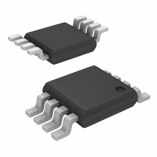
High Speed Operations : tpd = 1.5ns TYP (VCC=5V) Operating Voltage Range : 2V ~ 5.5V Low Power Consumption : 2µA (max) Small Package : MSOP-8B
■Pin Configuration
OUT IN C
IN
■Functions
8 7 6 5
VCC
OUT IN C
COM INH GND GND
1 2 3 4
CONTROL INPUT INH A H L L X H L
ON CHANNEL NONE Y1 Y0
Y0 Y1
A
H = High Level L = Low Level X = Don't care
MSOP-8B (TOP VIEW)
■Absolute Maximum Ratings
PARAMETER SYMBOL VCC VCONT Vi/o IIK IOK Ii/O ICC, IGND Pd Tstg RATINGS −0.5∼+6.0 −0.5∼+6.0
Ta=−40℃∼85℃ UNITS V V V mA mA mA mA mW ℃
13
Power Supply Voltage Control Input Voltage Switch Input/Output Voltage Control Input Diode Current Switch Output Diode Current Switch Input/Output Current VCC, GND Current Power Dissipation (Ta = 25℃) Storage Temperature
−0.5∼VCC+0.5 −20 ±20 ±25 ±50 300 −65∼+150
Note; Voltage is all Ground standardized.
944
�XC74WL4053SR
■Recommended Operating Conditions
PARAMETER Supply Voltage Control Input Voltage Switch Input/Output Voltage Operating Temperature Input Rise and Fall Time SYMBOL VCC VCONT Vi/o Topr tr, tf CONDITIONS 2∼5.5 0∼5.5 0∼VCC −40∼+85 0∼200(VCC=3.3V) 0∼100(VCC=5V) UNITS V V V ℃ ns
■DC Electrical Characteristics
PARAMETER SYMBOL VCC (V) 2.0 VIH Control Input Voltage VIL 3.0 5.5 2.0 3.0 5.5 2.0 Peak ON Resistance RONmax 3.0 4.5 2.0 ON Resistance RON(1) 3.0 4.5 2.0 Switch ON Resistance Differential △RON 3.0 4.5 Power Off Leakage Current IS(OFF) Power On Leakage Current Control Input Current Quiscent Supply Current IS(ON) IINH ICC 5.5 5.5 0∼5.5 5.5 VINH=VIL VCOM=0∼VCC ICOM=1mA VINH=VIL VCOM=GND or VCC ICOM=1mA VINH=VIL VCOM=0∼VCC ICOM=1mA VINH=VIH, VCOM=VCC, VY=GND VINH=VIL, VCOM=VCC or GND VCOM=VCC or GND VCOM=VCC or GND CONDITIONS MIN 1.5 2.1 3.85 − − − − − − − − − − − − − − − − Ta=25℃ TYP − − − − − − 130 22 12 23 14 10 13 3 2 − − − − MAX − − − 0.5 0.9 1.65 350 50 25 50 30 20 35 6 4 ±0.1 ±0.1 ±0.1 2.0 Ta=−40∼85℃ MAX MIN 1.5 2.1 3.85 − − − − − − − − − − − − − − − − − − − 0.5 0.9 1.65 550 65 35 65 40 25 55 8 6 ±0.1 ±0.1 ±0.1 20.2 μA μA μA μA Ω Ω Ω V V UNITS
13
945
�XC74WL4053SR
■Switching Electrical Characteristics
PARAMETER SYMBOL CL VCC (V) 2.0 15pF tPLH Propagation Delay Time tPHL 50pF 3.3 5.0 2.0 3.3 5.0 2.0 15pF Output Enable Time tZL tZH 50pF 3.3 5.0 2.0 3.3 5.0 2.0 15pF tLZ Output Disable Time tHZ 50pF 3.3 5.0 2.0 3.3 5.0 RL=10kΩ Sine Wave Distortion Rate 50pF 3.0 fCOM=1kHz − 0.05 − RL=1kΩ RL=1kΩ RL=1kΩ RL=1kΩ CONDITIONS MIN − − − − − − − − − − − − − − − − − − Ta=25℃ MAX TYP 2.5 2 1.5 4 3 2 8.5 4.5 3.5 9 5 4 9 7 6 12 10 8 12 4 3 20 6 5 45 9 7.5 50 10 8.5 45 17 14 60 23 20
(tr=tf=3ns) Ta=−40∼85℃ UNITS MAX MIN − − − − − − − − − − − − − − − − − − 15 5.5 4 23 8 6 60 11 9 65 12 10 55 20 18 75 27 25 ns ns ns ns ns ns
−
−
%
RL=600kΩ -3dB Band Width 50pF 3.0 20log10 VY VCOM Feed Through (Switch off) 50pF 3.0 RL=600kΩ − −60 − − − dB =−3dB − 200 − − − MHz
Cross Talk (Control Switch) 50pF
2.0 3.0 4.5
RL=600kΩ fINH=1MHz
− − −
60 100 150 −60 −60 −60 5 6 0.5 13
− − − − − − 10 − − −
− − − − − − − − − −
− − − − − − 10 − − − pF pF pF pF dB mV
Cross Talk (between Switches) 50pF
2.0 3.0 4.5
RL=600kΩ fCOM=1kHz
− − − − − − −
13
Control Input Capacitance
CINH
− − − −
− − − −
Switch Input/Output Capacitance CCOM/Y Feed Through Capacitance Power Dissipation Capacitance CCOM-Y Cpd
946
�XC74WL4053SR
■ON Resistance
ITypical Application Circuit
VCC VINH=VIL
INH INPUT COM(ON) GND
VCC Y VCOM-Y 10-3 OUTPUT
RON= 1.0mA V VCOM-Y
(Ω)
IVoltage Dependancies of ON Resistance
RON
RONmax
RON(1)
VCOM 0 VCC
13
947
�XC74WL4053SR
■Power Off Leakage Current
VCC
VINH=VIH
VCC
INH
VCC
A
COM(OFF) GND
Y
VCC
■Power On Leakage Current
VCC VINH=VIL
VCC
INH A COM(ON)
VCC Y OPEN
GND
13
948
�XC74WL4053SR
■Propagation Delay Time
ITypical Application Circuit
VCC VINH=VIL
INPUT INH Pulse Generator RIN= 50Ω VCC Y OUTPUT
COM(ON) GND
CL
IWaveforms
tr 90% 90% 50% 10% tPLH tPHL tf
VCC fCOM=1MHz tr=tf=3ns GND VOH
INPUT
10%
50%
OUTPUT
50%
50%
VOL
13
949
�XC74WL4053SR
■Output Enable Time, Output Disable Time
ITypical Application Circuit
RIN= 50Ω Pulse Generator VCC VCC
INPUT INH COM GND VCC Y RL= 1kΩ OUTPUT
CL
VCC
IWaveforms
tr 90% 90% 50% 10% tZH tHZ 90% tf
VCC fINH=1MHz tr=tf=3ns GND VOH
INPUT
10%
50%
OUTPUT
tZL
50% tLZ
VOL VOH
OUTPUT
50% 10%
13
VOL
950
�XC74WL4053SR
■Sine Wave Distortion Rate
VINH=VIL VCC INPUT RL= 10kΩ 10μF fCOM INH VCC Y OUTPUT VCC/2
COM(ON) GND
RIN= 50kΩ
CL= 50pF
* fCOM by sine wave (f=1kHz)
■-3dB Band Width
VINH=VIL VCC INPUT VCC/2
0.1μF fCOM
INH
VCC Y
RL= 600Ω
COM(ON) GND
OUTPUT
RIN= 50kΩ
CL= 50pF
* fCOM by sine wave (VCOM=VCC/10[Vp-p])
13
951
�XC74WL4053SR
■Feed Through Test Circuit
VINH=VIH VCC VCC/2 INPUT RL= 600Ω OUTPUT CL= 50pF
0.1μF fCOM RIN= 50Ω RIN= 600Ω
INH
VCC Y
COM(OFF) GND
VCC/2 * fCOM by sine wave (f=1MHz)
■Cross Talk (Control Input → Switch Output)
ITypical Application Circuit
INPUT RIN= 50Ω INH VCOM RL= 600Ω COM GND VCC Y CL= 50pF VCC VCC/2 Pulse Generator
RL= 600Ω OUTPUT
VCC/2
IWaveforms
13
INPUT
10%
tr 90% 90%
tf
VCC fINH=1MHz tr=tf=3ns
10%
GND
952
�XC74WL4053SR
■Cross Talk (between Switches)
ITypical Application Circuit
VINH=VIL VCC INPUT VCC/2
RL= 600Ω VCC INH (ON) Y0 COM (OFF) Y1 GND RL= 600Ω
CL=50pF OUTPUT1 OUTPUT2 CL=50pF
0.1μF fCOM RIN= 50Ω RIN= 600Ω
VCC/2
IWaveforms
tr 90% 90% tf
VCC fCOM=1MHz tr=tf=3ns
INPUT
10% 10%
GND
13
953
�
很抱歉,暂时无法提供与“XC74WL4053SR”相匹配的价格&库存,您可以联系我们找货
免费人工找货