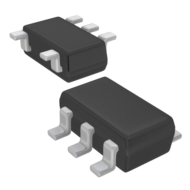
XC9110/XC9111 Series
ETR04006-008a
PFM Controlled Step-Up DC/DC Converter / Controller ICs
■GENERAL DESCRIPTION
The XC9110/9111 series is a group of PFM controlled step-up DC/DC converter/controller ICs designed to generate low supply
voltage by the combination of PFM control and CMOS structure. The series is ideal for applications where a longer battery life is
needed such as in portable communication equipment. With a built-in 2.5Ω N-channel driver transistor, the XC9110A/C/E and
XC9111A/C/E types provide a step-up operation by using only a coil, a capacitor, and a diode connected externally.
The XC9110/9111B, D and F versions can be used with an external transistor for applications requiring larger currents.
Output voltage is internally programmable in a range from 1.5V to 7.0V in increments of 0.1V (accuracy: ± 2.5%).
Maximum oscillation frequency is set to 100kHz for XC9110/9111 series. (At light loads, it is set to 180kHz for the XC9111
series.) Options include products equipped with a CE pin (C and D versions) that allows the IC to be shut down thereby
reducing supply current and with separated VDD/VOUT pins (E and F versions) to separate the power supply block and the
output voltage detect block. With the XC9110 series, maximum duty cycle is set to 75% (VDD=3.3V) making it suitable for use
with large current operations. The XC9111 series automatically switches duty ratio between 56% & 75% (VDD=3.3V) when it
senses changes in load to drop output ripple voltage and can support both large and small currents. The external transistor
types (B/D/F types) can be provided for applications, which require larger currents.
■APPLICATIONS
■ FEATURES
●Smart phones / Mobile phones
●Note PCs / Tablet PCs
●Digital still cameras / Camcorders
●Mobile devices / terminals
Input Voltage Range
: operating hold voltage 0.7V~10.0V
Start-up voltage
0.9V~10.0V
Output Voltage Range
: 1.5V ~ 7.0V in 0.1V increments
Output Accuracy
: ±2.5%
Max Oscillation Frequency : 100 kHz ±15%
180 kHz (at 56% duty of XC9111)
Built-in Switch Types
: A/C/E type
N-ch FET On-Resistance
: 2.5Ω@ VDD=3.0V
External Transistor Types
: B/D/F type
Lx Limit Voltage
: E type: more than VDD=2.0V
: A/C type: more than VOUT=2.0V
Max Duty Cycles
: 75% (for XC9110)
: 56%/75% two steps (for XC9111)
Low Supply Current
: 2.0μA @ VOUT=3V
Operating Ambient Temperature: -40℃ ~ 85℃
Packages
: SOT-23, SOT-89 (for XC9111),
SOT-25, USP-6C
■TYPICAL APPLICATION CIRCUIT
■TYPICAL PERFORMANCE
●C type circuit
CHARACTERISTICS
5
L
4
100
(TOP VIEW)
SOT-25
80
CIN
2
1
3
VOUT
SD
CE
+
CL
(Tantalum)
GND
Efficiency:EFFI(%)
VIN +
XC9111E331MR
L=100μH(CR54), CL47μF(Tantalum)
SD: XBS104S14R-G
2.4V
60
3.0V
1.5V
40
VIN=0.9V
1.2V
20
0
0
50
1 00
150
2 00
Output Current:IOUT(mA)
250
3 00
1/35
�XC9110/XC9111 Series
■BLOCK DIAGRAMS
●XC9111 A and B series
VDD
VLx limiter
Only A type
Lx
Vref
Buffer
VSS
VOUT
PFM Control OSC
100kHz (180kHz)
+
DUTY Selector
EXT
PFM Comparator
Note: The XC9110 series, Tr. Built-in type, uses the Lx pin and the XC9111 series, external Tr. Type, uses the EXT pin.
The duty ratio of the XC9111 series automatically varies between 56% (oscillation frequency 180kHz) and 75% (oscillation
frequency (fOSC) 100kHz). The VLx limit function only applies to the XC9110/9111 A types.
* The duty ratio depends on power supply. Please refer to the electrical characteristics on duty against output voltage you
use.
●XC9110 / 9111 C and D series
VDD
VLx limiter
Only C type
Lx
Vref
Buffer
VSS
VOUT
PFM Control OSC
100kHz (180kHz)
EXT
CE
DUTY Selector
Only XC9111
+
PFM Comparator
Chip Enable
Note: The XC9110 series, Tr. Built-in type, uses the Lx pin and the XC9111 series, external Tr. Type, uses the EXT pin.
The XC9110 series' duty ratio is 75% and oscillation frequency (fOSC) is 100kHz. The duty ratio of the XC9111 series
automatically varies between 56% (oscillation frequency 180kHz) and 75% (oscillation frequency (fOSC) 100kHz). The VLx
limit function only applies to the XC9110/9111 C versions.
* The duty ratio depends on power supply. Please refer to the electrical characteristics on duty against output voltage you
use.
2/35
�XC9110/XC9111
Series
■BLOCK DIAGRAMS
●XC9111 E and F series
VDD
VDD
VLx limiter
Only E type
Lx
Vref
Buffer
PFM Control OSC
100kHz(180kHz)
VSS
VOUT
DUTY Selector
Only XC9111
+
PFM Comparater
EXT
Note: The XC9110 series, Tr. Built-in type, uses the Lx pin and the XC9111 series, external Tr. Type, uses the EXT pin.
The XC9110 / 9111 series E and F series have the VDD pin. The XC9110 series' duty ratio is 75% and
oscillation frequency (fOSC) is 100kHz. The duty ratio of the XC9111 series automatically varies between
56% (oscillation frequency 180kHz) and 75% (oscillation frequency (fOSC) 100kHz).
The VLx limit function only applies to the XC9110/9111 C versions.
* The duty ratio depends on power supply.
Please refer to the electrical characteristics on duty against output voltage you use.
3/35
�XC9110/XC9111 Series
■PRODUCT CLASSIFICATION
●Ordering Information
XC9110①②③④⑤⑥-⑦ : PFM control, 75% duty
XC9111①②③④⑤⑥-⑦ : PFM control, 56% / 75% duty variable
DESIGNATOR
①
CE Function
②③
Output Voltage
Maximum Oscillation
Frequency
④
⑤⑥-⑦(*1)
(*1)
ITEM
Packages
(Order Unit)
SYMBOL
A
B
C
D
E
F
15 ~ 70
1
MR-G
PR-G
ER-G
DESCRIPTION
VDD / VOUT common type (for XC9111series)
VDD / VOUT common type (for XC9111series)
CE pin (5 pin)
CE pin (5 pin)
VDD / VOUT separated type (5 pin)
VDD / VOUT separated type (5 pin)
ex. 3.5V output → ②= 3, ③= 5
100kHz
①=A ~ B SOT-23 (3,000pcs/Reel)
①=C ~ F SOT-25 (3,000pcs/Reel)
①=A ~ B SOT-89 (1,000pcs/Reel)
①=C ~ F USP-6C (3,000pcs/Reel)
The “-G” suffix denotes Halogen and Antimony free as well as being fully EU RoHS compliant.
●Selection Guide
4/35
Built-in Transistor
External Transistor
Built-in Transistor
External Transistor
Built-in Transistor
External Transistor
�XC9110/XC9111
Series
■PIN CONFIGURATION
Lx/EXT
VOUT
VSS
5
3
1
2
VSS
Lx/EXT
4
1
2
3
CE/VOUT VOUT/VDD NC
SOT-23 (TOP VIEW)
SOT-25 (TOP VIEW)
1
2
3
VSS
VOUT
Lx/EXT
SOT-89 (TOP VIEW)
VSS
6
1 VOUT/VDD
NC
5
2
4
3
Lx/EXT
NC
CE/VOUT
USP-6C (BOTTOM VIEW)
*The dissipation pad for the USP-6C package should be solder-plated in recommended mount pattern
and metal masking so as to enhance mounting strength and heat release. If the pad needs to be
connected to other pins, it should be connected to the pin No.1.
■PIN ASSIGNMENT
●XC9111A/B
PIN NUMBER
SOT-23
SOT-89
A
B
A
B
1
1
1
1
3
3
2
2
2
3
2
3
PIN NAME
VSS
VOUT
LX
EXT
FUNCTIONS
Ground
Output Voltage Montior, Internal Power Supply
Switch
External Switching transistor drive
The PFM comparator compares the feedback voltage divided by the internal split resistors with the internal reference
voltage. When the feedback voltage is higher than the reference voltage, PFM controlled OSC will be stopped. When the
feedback voltage is lower than the reference voltage, the PFM controlled OSC will be operated so that the output voltage
will be stable by sending a signal to the buffer drive circuit and controlling the internal or external driver transistor.
< Duty Selector >
With the XC9111 series, the duty selector automatically switches duty ratio between 56% and 75% when it senses
changes in load and can support both large and small currents.
< PFM Controlled Oscillator >
The PFM controlled OSC determines maximum oscillation frequency. The circuit generates the oscillation frequency of
100kHz at 75% duty and 180kHz at 56%.
< VLx Limiter>
The VLx circuit of the XC9110/9111 A, C and D types detects in-rush current and overcurrent, which flows from the VOUT
pin to the Lx pin during short-circuit. In overcurrent, the driver transistor will be OFF. When the overcurrent state is
eliminated, the IC resumes its normal operation.
The chip enable function of the XC9110/9111 C and D types enables the IC to be in shut down mode when a low level
signal is input to the CE pin. During the shutdown mode, the current consumption will be reduced to 0.5μA (MAX.).
With the separated VDD pin, the XC9110/9111 E and F types can be operated in both low and high voltage.
16/35
�XC9110/XC9111
Series
■EXTERNAL COMPONENTS
Tr.: *Using a MOSFET
XP151A13A0MR-G (N-ch Power MOSFET, TOREX)
Note : VGS breakdown voltage of this Transistor is 8V
so please be careful with the power supply voltage.
If the power supply voltage is over 6V, Please use the
XP151A12A2MR-G with a VGS breakdown voltage of 12V.
* Using a NPN Transistor
2SD1628 (SANYO)
RB: 500Ω (Adjust in accordance with load and Tr’s hFE.)
CB: 2200pF (Ceramic)
CB ≦1 / ( 2TT x RB x FOSC x 0.7 )
●RB value example (when using NPN Transistor)
VOUT (V)
IOUT (mA)
VIN (V)
RB (Ω)
VOUT (V)
IOUT (mA)
VIN (V)
RB (Ω)
1.8
1.8
1.8
1.8
1.8
1.8
10
10
30
30
50
50
1.2
1.5
1.2
1.5
1.2
1.5
4.5
6.0
2.0
2.0
1.2
1.5
3.3
3.3
3.3
3.3
3.3
3.3
5
5
10
10
30
30
1.2
1.5
1.2
1.5
1.2
1.5
6.5
6.5
5.0
4.5
3.5
3.5
* Tr.: 2SD1628
SD: XBS104S14R-G (TOREX)
MA2Q735
(MATSUSHITA)
(Tantalum type, KYOCERA TAJ)
CL: 16V, 47μF
(Tantalum type, KYOCERA TAJ)
CIN: 16V, 47μF
16V, 220μF
(Electrolytic Capacitor)
L:
100μH
(CR54,SUMIDA)
100μH
(CDRH6D28,SUMIDA)
22μH, 47μH
(CR54, SUMIDA)
■NOTES ON USE
1. Please do not exceed the value of stated absolute maximum ratings.
2. The DC/DC converter / controller IC's performance is greatly influenced by not only the ICs' characteristics, but also
by those of the external components. Care must be taken when selecting the external components.
3. The Lx limit voltage function becomes stable when VOUT of the XC9110/9111C series is over 2.0V and the VDD of the
XC9110/9111E series is over 2.0V.
4. Make sure that the PCB GND traces are as thick as possible, as variations in ground potential caused by high ground
currents at the time of switching may result in instability of the IC.
5. Please mount each external component as close to the IC as possible and use thick, short connecting traces to reduce
the circuit impedance.
17/35
�XC9110/XC9111 Series
■TEST CIRCUITS
Circuit ①
Circuit ⑤
Circuit ②
Circuit ⑥
Circuit ③
Circuit ⑦
Circuit ④
Circuit ⑧
Circuit ①
CIN: 47μF, 16V
L: CR54, 100μH
SD: XBS104S14R-G
CL: 47μF, 16V
Circuit②
Rp: 300Ω
Rp: 10Ω
Rp: 200Ω
Cp: 100μF
18/35
(Tantalum)
(SUMIDA)
(Schottky, TOREX)
(Tantalum)
(For Lx ON Resistance
and measuring Lx Limit Current)
(For measuring EXT ON Resistance)
(OS-CON, SANYO)
Circuit ④
Cp: 100μF
(OS-CON, SANYO)
Circuit ⑥
CIN: 47μF, 16V
(Tantalum)
L: CR54, 100μH (SUMIDA)
Tr: 2SD1628
(SANYO)
CB: 2200pF
RB: 500Ω
SD: XBS104S14R-G (Schottky, TOREX)
CL: 47μF, 16V
(Tantalum)
�XC9110/XC9111
Series
■TYPICAL PERFORMANCE CHARACTERISTICS
*Topr = 25℃
(1) Output Voltage vs. Output Current
XC9111E181MR
1.9
1.8
VIN=0.9V
1.7
1.2V
1.5V
1.6
L=100uH(CR54),CL:47uF(Tantalum)
SD:XBS104S14R
2
Output Voltage: V OUT(V)
2
Output Voltage:V OUT(V)
XC9110E181MR
L=100uH(CR54),CL:47uF(Tantalum)
SD:XBS104S14R
1.5
1.9
1.2V
1.8
VIN=0.9V
1.7
1.6
1.5
0
20
40
60
80
Output Current:IOUT(mA)
100
0
2.4V
2.5
1.5V
1.2V
2
VIN=0.9V
1.5
60
80
100
L=100uH(CR54),CL:47uF(Tantalum)
SD:XBS104S14R
3.5
Output Voltage: V OUT(V)
Output Voltage:V OUT(V)
3.0V
3
40
XC9110E331MR
L=100uH(CR54),CL:47uF(Tantalum)
SD:XBS104S14R
3.5
20
Output Current:IOUT(mA)
XC9111E331MR
3.0V
3
1.5V
1.2V
2.5
2.4V
VIN=0.9V
2
1.5
1
1
0
50
100
150
200
250
0
300
100
150
200
250
Output Current:IOUT(mA)
XC9111E501MR
XC9110E501MR
L=100uH(CR54),CL:47uF(Tantalum)
SD:XBS104S14R
4.9
2.7V
3.3V
4.2V
VIN=1.5V
4.7
4.6
300
L=100uH(CR54),CL:47uF(Tantalum)
SD:XBS104S14R
5.1
Output Voltage: V OUT(V)
5
4.8
50
Output Current:IOUT(mA)
5.1
Output Voltage: V OUT(V)
1.5V
5
2.7V
4.9
3.3V
4.2V
4.8
VIN=1.5V
4.7
4.6
0
50
100
150
200
250
Output Current:IOUT(mA)
300
0
50
100
150
200
250
300
Output Current:IOUT(mA)
19/35
�XC9110/XC9111 Series
■TYPICAL PERFORMANCE CHARACTERISTICS (Continued)
(1) Output Voltage vs. Output Current (Continued)
*Topr = 25℃
XC9111F181MR
1.9
1.5V
VIN=1.2V
1.8
1.7
1.6
L=22uH(CR54),CL:47uF(Tantalum)
SD:XBS104S14R,Tr:XP151A13A0M
3.8
Output Voltage:V OUT(V)
2.0
Output Voltage:V OUT(V)
XC9111F331MR
L=22uH(CR54),CL:47uF(Tantalum)
SD:XBS104S14R,Tr:XP151A13A0M
3.6
3.0V
3.4
VIN=1.5V
3.2
3.0
2.8
1.5
0
100
200
300
Output Current:IOUT(mA)
0
400
XC9111F501MR
3.3V
4.9
2.7V
VIN=2.4V
4.8
4.7
4.6
0
100
200
300
Output Current:IOUT(mA)
400
400
L=22uH(CR54),CL:47uF(Tantalum),CB:2200pF
SD:XBS104S14R,Tr:2SD1628,RB:100omh
2.0
Output Voltage:V OUT(V)
Output Voltage:V OUT(V)
5.0
100
200
300
Output Current:IOUT(mA)
XC9111F181MR
L=22uH(CR54),CL:47uF(Tantalum)
SD:XBS104S14R,Tr:XP151A12A2M
5.1
20/35
2.4V
1.5V
1.9
VIN=0.9V
1.8
1.2V
1.7
1.6
1.5
0
100
200
300
Output Current:IOUT(mA)
400
�XC9110/XC9111
Series
■TYPICAL PERFORMANCE CHARACTERISTICS (Continued)
(2) Efficiency vs. Output Current
*Topr = 25℃
XC9111E181MR
100
80
60
1.2V
VIN=0.9V
40
1.5V
20
L=100uH(CR54),CL:47uF(Tantalum)
SD:XBS104S14R
100
Efficiency:EFFI(%)
Efficiency:EFFI(%)
XC9110E181MR
L=100uH(CR54),CL:47uF(Tantalum)
SD:XBS104S14R
80
60
1.2V
20
0
0
0
20
40
60
80
Output Current:IOUT(mA)
0
100
2.4V 3.0V
1.5V
40
1.2V
VIN=0.9V
20
60
80
100
L=100uH(CR54),CL:47uF(Tantalum)
SD:XBS104S14R
100
Efficiency:EFFI(%)
Efficiency:EFFI(%)
80
60
40
XC9110E331MR
L=100uH(CR54),CL:47uF(Tantalum)
SD:XBS104S14R
100
20
Output Current:IOUT(mA)
XC9111E331MR
80
3.0V
2.4V
60
1.5V
40
VIN=0.9V
20
1.2V
0
0
0
50
100
150
200
250
0
300
150
200
250
XC9111E501MR
XC9110E501MR
VIN=1.5V
60
100
Output Current:IOUT(mA)
2.7V
3.3V
4.2V
40
20
0
300
L=100uH(CR54),CL:47uF(Tantalum)
SD:XBS104S14R
100
Efficiency:EFFI(%)
80
50
Output Current:IOUT(mA)
L=100uH(CR54),CL:47uF(Tantalum)
SD:XBS104S14R
100
Efficiency:EFFI(%)
1.5V
VIN=0.9V
40
80
VIN=1.5V
60
2.7V
3.3V
4.2V
40
20
0
0
50 100 150 200 250
Output Current:IOUT(mA)
300
0
50 100 150 200 250
Output Current:IOUT(mA)
300
21/35
�XC9110/XC9111 Series
■TYPICAL PERFORMANCE CHARACTERISTICS (Continued)
(2) Efficiency vs. Output Current (Continued)
*Topr = 25℃
XC9111F181MR
80
1.5V
VIN=1.2V
60
40
20
0
80
VIN=1.5V
2.4V
60
40
20
100
200
300
Output Current:IOUT(mA)
400
0
XC9111F501MR
80
100
Efficiency:EFFI(%)
2.7V,3.3V
VIN=2.4V
60
40
20
0
100
200
300
Output Current:IOUT(mA)
400
XC9111F181MR
L=22uH(CR54),CL:47uF(Tantalum)
SD:XBS104S14R,Tr:XP151A12A2M
100
Efficiency:EFFI(%)
3.0V
0
0
L=22uH(CR54),CL:47uF(Tantalum),CB:2200pF
SD:XBS104S14R,Tr:2SD1628,RB:100ohm
80
1.5V
60
VIN=0.9V
40
1.2V
20
0
0
22/35
L=22uH(CR54),CL:47uF(Tantalum)
SD:XBS104S14R,Tr:XP151A13A0M
100
Efficiency:EFFI(%)
100
Efficiency:EFFI(%)
XC9111F331MR
L=22uH(CR54),CL:47uF(Tantalum)
SD:XBS104S14R,Tr:XP151A13A0M
100
200
300
Output Current:IOUT(mA)
400
0
100
200
300
Output Current:IOUT(mA)
400
�XC9110/XC9111
Series
■TYPICAL PERFORMANCE CHARACTERISTICS (Continued)
*Topr = 25℃
(3) Ripple Voltage vs. Output Current
XC9111E181MR
120
100
80
60
1.2V
40
1.5V
20
VIN=0.9V
0
0
L=100uH(CR54),CL:47uF(Tantalum)
SD:XBS104S14R
120
Ripple Voltage:Vr(mV)
Ripple Voltage:Vr(mV)
XC9110E181MR
L=100uH(CR54),CL:47uF(Tantalum)
SD:XBS104S14R
100
80
60
40
1.2V
20
VIN=0.9V
0
20
40
60
80
Output Current:IOUT(mA)
100
0
80
60
1.5V
2.4V
1.2V
20
VIN=0.9V
0
0
100
60
1.2V
20
VIN=0.9V
0
4.2V
2.7V
VIN=1.5V
0
0
50
100
150
200
250
150
200
250
300
L=100uH(CR54),CL:47uF(Tantalum)
SD:XBS104S14R
120
100
4.2V
80
3.3V
60
2.7V
40
20
VIN=1.5V
0
Output Current:IOUT(mA)
100
XC9110E501MR
Ripple Voltage:Vr(mV)
Ripple Voltage:Vr(mV)
3.3V
20
50
Output Current:IOUT(mA)
100
40
2.4V
1.5V
40
300
L=100uH(CR54),CL:47uF(Tantalum)
SD:XBS104S14R
60
100
3.0V
80
XC9111E501MR
80
80
120
0
50 100 150 200 250
Output Current:IOUT(mA)
120
60
L=100uH(CR54),CL:47uF(Tantalum)
SD:XBS104S14R
140
Ripple Voltage:Vr(mV)
Ripple Voltage:Vr(mV)
3.0V
40
40
XC9110E331MR
L=100uH(CR54),CL:47uF(Tantalum)
SD:XBS104S14R
100
20
Output Current:IOUT(mA)
XC9111E331MR
120
1.5V
300
0
50 100 150 200 250
Output Current:IOUT(mA)
300
23/35
�XC9110/XC9111 Series
■TYPICAL PERFORMANCE CHARACTERISTICS (Continued)
(3) Ripple Voltage vs. Output Current (Continued)
XC9111F331MR
XC9111F181MR
L=22uH(CR54),CL:47uF(Tantalum)
SD:XBS104S14R,Tr:XP151A13A0M
200
VIN=1.2V
1.5V
150
100
50
Ripple Voltage:Vr(mV)
Ripple Voltage:Vr(mV)
250
0
0
100
200
300
Output Current:IOUT(mA)
200
100
2.7V
100
VIN=2.4V
50
0
0
100
200
300
Output Current:IOUT(mA)
24/35
400
100
200
300
Output Current:IOUT(mA)
400
XC9111F181MR
350
Ripple Voltage:Vr(mV)
Ripple Voltage:Vr(mV)
150
VIN=1.5V
50
0
L=22uH(CR54),CL:47uF(Tantalum)
SD:XBS104S14R,Tr:XP151A12A2M
3.3V
3.0V
0
400
200
2.4V
150
XC9111F501MR
250
L=22uH(CR54),CL:47uF(Tantalum)
SD:XBS104S14R,Tr:XP151A13A0M
250
L=22uH(CR54),CL:47uF(Tantalum),CB:2200pF
SD:XBS104S14R,Tr:2SD1628,RB:100ohm
300
1.5V
250
1.2V
200
150
100
VIN=0.9V
50
0
0
100
200
300
Output Current:IOUT(mA)
400
*Topr = 25℃
�XC9110/XC9111
Series
■TYPICAL PERFORMANCE CHARACTERISTICS (Continued)
(4) Supply Current 1 vs. Output Voltage
XC9111E**1
70
Supply Current2: ID D 2(uA)
Supply Current1: ID D 1(uA)
XC9111E**1
VDD=V OUT×0.95
80
Topr=85OC
25OC
-40OC
60
50
40
30
20
10
0
1.5
2.5
3.5
4.5
5.5
VDD=V OUT+0.5
5
4.5
4
3.5
3
2.5
2
1.5
1
0.5
0
Topr=85OC
25OC
-40OC
1.5
6.5
2.5
85OC
Topr= 25O,-40OC
3.5
4.5
5.5
80
70
60
85OC
50
40
30
20
0
1.5
3.5
4.5
5.5
6.5
(9) Lx Switch-ON Resistance vs. Output Voltage
XC9111E∗∗1
VDD=V OUT×0.95
1
0.9
Topr=85OC
25OC
-40OC
VDD=V OUT×0.95,VLx=0.4V
7
Lx Switch-ON
Resistance:RSWON ( Ω )
Lx Limit Voltage: VLxLMT(V)
2.5
Output Voltage:V OUT(V)
XC9111E**1
0.7
Topr= 25OC
-40OC
V IN =V OUT×0.6
10
6.5
(8) Lx Limit Voltage vs. Output Voltage
0.8
6.5
L=100uH(CR54),CL:47uF(Tantalum)
SD:XBS104S14R
Output Voltage:V OUT(V)
1.1
5.5
XC9111E**1
( uA)
No-Load Input Current: IIN
Stand-by Current: ISTB(uA)
XC9111C**1
2.5
4.5
(7) No Load Input Current vs. Output Voltage
(6) Stand-by Current vs. Output Voltage
1.5
3.5
Output Voltage:V OUT(V)
Output Voltage:V OUT(V)
0.5
0.45
0.4
0.35
0.3
0.25
0.2
0.15
0.1
0.05
0
*Topr = 25℃
(5) Supply Current 2 vs. Output Voltage
Topr=85OC
25OC
-40OC
6
5
4
3
2
1
0
0.6
2
3
4
5
6
Output Voltage:V OUT(V)
7
1.5
2.5
3.5
4.5
5.5
6.5
Output Voltage:V OUT(V)
* The reason for the increase in the "no load input current" figure at Ta=85℃ in the performance characteristics is
because of an increase in the reverse current of the Schottky diode and not because of abnormalities of the IC itself.
25/35
�XC9110/XC9111 Series
■TYPICAL PERFORMANCE CHARACTERISTICS (Continued)
*Topr = 25℃
(10) EXT H ON Resistance vs. Output Voltage
(11) EXT L ON Resistance vs. Output Voltage
(12) Maximum Oscillation Frequency 1. vs. Output Voltage
(13) Maximum Oscillation Frequency 2 vs. Output Voltage
(14) Duty Ratio 1 vs. Output Voltage
(15) Duty Ratio 2 vs. Output Voltage
26/35
�XC9110/XC9111
Series
■TYPICAL PERFORMANCE CHARACTERISTICS (Continued)
(16) Output Voltage vs. Ambient Temperature
(17) CE “H”, “L” Voltage vs. Output Voltage
XC9111E331
XC9111C∗∗1
3.4
3.3
3.2
3
-50
VDD=V OUT×0.95
0.80
CE "H","L"Voltage:VCEH,L(V)
Output Voltage: V OUT(V)
3.5
3.1
VIN=1.98V
IOUT=30mA
-20
10
40
70
100
0.70
-40OC
0.60
0.50
0.40
85OC
0.30
Topr=25OC
0.20
0.10
0.00
1.5
Ambient Temp:Ta( oC)
40
4.5
5.5
6.5
70
100
XC9111E331
Osillation Start Voltage:V ST2(V)
Operation Start Voltage:V ST1(V)
IOUT=1.0mA
10
3.5
(19) Oscillation Start Voltage vs. Ambient Temperature
XC9111E331
L=100uH(CR54),CL=47uF(Tantalum)
SD:XBS104S14R
-20
2.5
Output Voltage:V OUT(V)
(18) Operation Start Voltage vs. Ambient Temperature
1
0.9
0.8
0.7
0.6
0.5
0.4
0.3
0.2
0.1
0
-50
*Topr = 25℃
1
0.9
0.8
0.7
0.6
0.5
0.4
0.3
0.2
0.1
0
-50
VOUT=0.8V
-20
10
40
70
100
Ambient Temp:Ta( oC)
o
Ambient Temp:Ta( C)
(20) Operation Hold Voltage vs. Ambient Temperature
XC9111E331
Operation Holding
Voltage:V HLD (V)
0.6
0.5
0.4
0.3
0.2
IOUT=1.0mA
0.1
0
-50
-20
10
40
70
100
o
Ambient Temp:( C)
27/35
�XC9110/XC9111 Series
■TYPICAL PERFORMANCE CHARACTERISTICS (Continued)
(21) Load Transient Response
VIN=2.4V, VDD=VOUT, IOUT=0.1mA
28/35
*Topr = 25℃
50mA
�XC9110/XC9111
Series
■TYPICAL PERFORMANCE CHARACTERISTICS (Continued)
(22) Input Transient Response
*Topr = 25℃
29/35
�XC9110/XC9111 Series
■PACKAGING INFORMATION
For the latest package information go to, www.torexsemi.com/technical-support/packages
PACKAGE
OUTLINE / LAND PATTERN
THERMAL CHARACTERISTICS
SOT-23
SOT-23 PKG
SOT-23 Power Dissipation
SOT-25
SOT-25 PKG
SOT-25 Power Dissipation
SOT-89
SOT-89 PKG
SOT-89 Power Dissipation
USP-6C
USP-6C PKG
USP-6C Power Dissipation
30/35
�XC9110/XC9111
Series
■ MARKING RULE
●SOT-23
① represents product series
MARK
FUNCTIONS
-
5
6
Built-In Transistor
External Transistor
PRODUCT SERIES
XC9111Axxxxx
XC9111Bxxxxx
② represents integer of output voltage and oscillation frequency
OUTPUT VOLTAGE
1.x
2.x
3.x
4.x
5.x
6.x
7.x
MARK
fOSC=100kHz
1
2
3
4
5
6
7
③ represents decimal point of output voltage and oscillation frequency
OUTPUT VOLTAGE
MARK
fOSC=100KHz
x.0
0
x.1
1
x.2
2
x.3
3
x.4
4
x.5
5
x.6
6
x.7
7
x.8
8
x.9
9
④ represents production lot number
0 to 9, A to Z repeated (G, I, J, O, Q, W excluded)
31/35
�XC9110/XC9111 Series
■ MARKING RULE (Continued)
●SOT-25
① represents product series
MARK
SOT-25 (TOP VIEW)
FUNCTION
V
X
Y
Z
5
6
7
8
CE
CE
VDD/VOUT
VDD/VOUT
CE
CE
VDD/VOUT
VDD/VOUT
PRODUCT SERIES
Tr. Built-in
External Tr.
Tr. Built-in
External Tr.
Tr. Built-in
External Tr.
Tr. Built-in
External Tr.
XC9110Cxxxxx
XC9110Dxxxxx
XC9110Exxxxx
XC9110Fxxxxx
XC9111Cxxxxx
XC9111Dxxxxx
XC9111Exxxxx
XC9111Fxxxxx
② represents integer of output voltage and oscillation frequency
OUTPUT VOLTAGE
MARK
fOSC=100kHz
1.x
2.x
3.x
4.x
5.x
6.x
7.x
1
2
3
4
5
6
7
③ represents decimal point of output voltage and oscillation frequency
OUTPUT VOLTAGE
MARK
fOSC=100kHz
x.0
x.1
x.2
x.3
x.4
x.5
x.6
x.7
x.8
x.9
0
1
2
3
4
5
6
7
8
9
④ represents production lot number
0 to 9, A to Z repeated (G, I, J, O, Q, W excluded)
32/35
�XC9110/XC9111
Series
■ MARKING RULE (Continued)
●SOT-89
① represents product series
MARK
-
5
6
FUNCTIONS
Built-In Transistor
External Transistor
PRODUCT SERIES
XC9111Axxxxx
XC9111Bxxxxx
② represents integer of output voltage and oscillation frequency
OUTPUT VOLTAGE
1.x
2.x
3.x
4.x
5.x
6.x
7.x
MARK
fOSC=100kHz
1
2
3
4
5
6
7
③ represents decimal point of output voltage and oscillation frequency
OUTPUT VOLTAGE
x.0
x.1
x.2
x.3
x.4
x.5
x.6
x.7
x.8
x.9
MARK
fOSC=100kHz
0
1
2
3
4
5
6
7
8
9
④ represents production lot number
0 to 9, A to Z repeated (G, I, J, O, Q, W excluded)
33/35
�XC9110/XC9111 Series
■ MARKING RULE (Continued)
●USP-6C
① represents product series
MARK
PRODUCT SERIES
M
N
XC9110xxx1Dx
XC9111xxx1Dx
② represents series type
USP-6C (TOP VIEW)
MARK
FUNCTION
C
D
E
F
CE
CE
VDD/VOUT
VDD/VOUT
PRODUCT SERIES
Tr. Built-in
External Tr.
Tr. Built-in
External Tr.
XC911xCxx1Dx
XC911xDxx1Dx
XC911xExx1Dx
XC911xFxx1Dx
③ represents integer of output voltage
MARK
OUTPUT VOLTAGE
1
2
3
4
5
6
7
1.x
2.x
3.x
4.x
5.x
6.x
7.x
④ represents decimal point of output voltage
MARK
OUTPUT VOLTAGE
0
1
2
3
4
5
6
7
8
9
x.0
x.1
x.2
x.3
x.4
x.5
x.6
x.7
x.8
x.9
⑤ represents oscillation frequency
MARK
OSCILLATION FREQUENCY
PRODUCT SERIES
1
x.0
XC911xxxx1Dx
⑥ represents production lot number
0 to 9, A to Z repeated (G, I, J, O, Q, W excluded)
* No character inversion used
34/35
�XC9110/XC9111
Series
1.
The product and product specifications contained herein are subject to change without notice to
improve performance characteristics. Consult us, or our representatives before use, to confirm that
the information in this datasheet is up to date.
2.
The information in this datasheet is intended to illustrate the operation and characteristics of our
products. We neither make warranties or representations with respect to the accuracy or
completeness of the information contained in this datasheet nor grant any license to any intellectual
property rights of ours or any third party concerning with the information in this datasheet.
3.
Applicable export control laws and regulations should be complied and the procedures required by
such laws and regulations should also be followed, when the product or any information contained in
this datasheet is exported.
4.
The product is neither intended nor warranted for use in equipment of systems which require
extremely high levels of quality and/or reliability and/or a malfunction or failure which may cause loss
of human life, bodily injury, serious property damage including but not limited to devices or equipment
used in 1) nuclear facilities, 2) aerospace industry, 3) medical facilities, 4) automobile industry and
other transportation industry and 5) safety devices and safety equipment to control combustions and
explosions. Do not use the product for the above use unless agreed by us in writing in advance.
5.
Although we make continuous efforts to improve the quality and reliability of our products;
nevertheless Semiconductors are likely to fail with a certain probability. So in order to prevent personal
injury and/or property damage resulting from such failure, customers are required to incorporate
adequate safety measures in their designs, such as system fail safes, redundancy and fire prevention
features.
6.
Our products are not designed to be Radiation-resistant.
7.
Please use the product listed in this datasheet within the specified ranges.
8.
We assume no responsibility for damage or loss due to abnormal use.
9.
All rights reserved. No part of this datasheet may be copied or reproduced unless agreed by Torex
Semiconductor Ltd in writing in advance.
TOREX SEMICONDUCTOR LTD.
35/35
�