XC9119D10A Series
ETR0408_009
1MHz, PWM Controlled,
Step-Up DC/DC Converter, Ceramic Capacitor Compatible
■GENERAL DESCRIPTION
The XC9119D10A series is 1MHz, PWM controlled step-up DC/DC converter, designed to allow the use of ceramic
capacitors. With a built-in 2.0Ω switching transistor, the XC9119D10A series can easily provide a step-up operation by using
only a coil, a diode, a capacitor, and a resistor, connected externally.
Since output voltage up to 19.5V (Maximum Lx operating voltage: 20V) can be derived with reference voltage supply of 1.0V
(±2.0%) and external components, the series can easily supply high voltage for various general-purpose power supplies, LCD
panels and organic EL displays.
With a high switching frequency of 1.0MHz, a low profile and small board area solution can be achieved using a chip coil and
an ultra small ceramic output capacitor.
With the current limit function (400mA (TYP.): VDD=3.6V), a peak current, which flows through built-in driver transistors can be
limited. Soft-start time can be adjusted by external resistors and capacitors. The stand-by function enables the output to
be turned off (CE ’L’), that is, the supply current will be less than 1.0μA.
■APPLICATIONS
●Organic electroluminescence display (OELD)
●Power supplies for LCDs
●Multi-function power supplies
■FEATURES
Operating Voltage Range : 2.5V ~ 6.0V
: Up to 19.5V externally set-up
Output Voltage Range
: Reference voltage 1.0V +2.0%
Oscillation Frequency
: 1.0MHz±20%
ON Resistance
: 2.0Ω (VDD=3.6V, VDS=0.4V)
Efficiency
: 86%
(VOUT=15V, VDD=3.6V, IOUT=10mA)
: PWM control
Stand-by function
: ISTB=1.0μA (MAX.)
Load Capacitor
: Low ESR ceramic capacitor
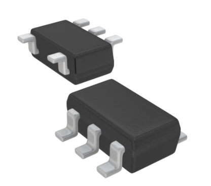
Ultra Small Packages
: SOT-25, USP-6C
Lx Limit Current
: 400mA (VDD=3.6V)
■TYPICAL PERFORMANCE
CHARACTERISTICS
○Efficiency vs. Output Current
XC9119D10A
Efficiency: EFFI(%)
■TYPICAL APPLICATION CIRCUIT
Control
100
90
80
70
60
50
40
30
20
10
0
6V
5V
4.2V
3.6V
VIN=2.5V
2.7V 3V
T a=25 o C
0.1
1
10
100
1000
Output Current: IOUT (mA)
1/18
�XC9119D10A Series
■PIN CONFIGURATION
*The dissipation pad for the USP-6C
package should be solder-plated in
recommended mount pattern and metal
masking so as to enhance mounting
strength and heat resistance. If the pad
needs to be connected to other pins, it
should be connected to the VSS pin.
USP-6C
(BOTTOM VIEW)
SOT-25
(TOP VIEW)
■PIN ASSIGNMENT
PIN NUMBER
SOT-25
USP-6C
1
2
3
4
5
-
2
3
1
6
4
5
PIN NAME
FUNCTION
Lx
VSS
FB
CE/SS
VDD
NC
Switch
Ground
Voltage Feedback
Chip Enable/ Soft Start
Power Input
No Connection
■CE PIN FUNCTION
CE/SS PIN
OPERATIONAL STATE
H
L
Operation
Shut-down
■PRODUCT CLASSIFICATION
●Ordering Information
XC9119D①②③④⑤-⑥(*1)
DESIGNATOR
ITEM
SYMBOL
①②
Reference Voltage
10
FB voltage
③
Oscillation Frequency
A
1MHz
④⑤-⑥
(*1)
DESCRIPTION
MR
SOT-25 (3,000/Reel)
Packages
MR-G
SOT-25 (3,000/Reel)
(Order Unit)
ER
USP-6C (3,000/Reel)
ER-G
USP-6C (3,000/Reel)
The “-G” suffix denotes Halogen and Antimony free as well as being fully EU RoHS compliant.
2/18
�XC9119D10A
Series
■BLOCK DIAGRAM
Phase
Compensation
VDD
Current
Limit & Feedback
Error Amp.
LX
+
FB
+
-
logic
Vref with
Soft-start,
CE
Buffer
Driver
PWM Comparator
VSS
Ramp Wave
Generator, OSC
CE/SS
■ABSOLUTE MAXIMUM RATINGS
Ta = 25OC
PARAMETER
SYMBOL
RATINGS
UNITS
VDD Pin Voltage
Lx Pin Voltage
VDD
VSS – 0.3 ~ 7.0
V
VLx
VSS – 0.3 ~ 22.0
V
FB Pin Voltage
VFB
VSS – 0.3 ~ 7.0
V
CE Pin Voltage
VCE
VSS – 0.3 ~ 7.0
V
Lx Pin Current
ILx
1000
mA
Power Dissipation
SOT-25
USP-6C
Pd
250
120
mW
Operating Ambient Temperature
Topr
- 40 ~ + 85
O
Storage Temperature
Tstg
- 55 ~ +125
O
C
C
3/18
�XC9119D10A Series
■ELECTRICAL CHARACTERISTICS
XC9119D10AMR
PARAMETER
SYMBOL
FB Voltage
VFB
△VFB/
△VIN・VFB
VDD
Line Regulation
Supply Voltage
Operation Start-up
Voltage
CONDITIONS
2.5
很抱歉,暂时无法提供与“XC9119D10AMR-G”相匹配的价格&库存,您可以联系我们找货
免费人工找货- 国内价格
- 1+3.38040
- 10+2.81880
- 30+2.57040
- 100+2.27880
- 500+1.69560
- 1000+1.60920


 工商网监
湘ICP备2023018690号
工商网监
湘ICP备2023018690号
