XC9120/XC9121/XC9122 Series
ETR0409-004
Step-Up DC/DC Controller IC, MAXDUTY: 93%
☆GreenOperation-Compatible
■GENERAL DESCRIPTION
XC9120/9121/9122 Series are PWM, PWM/PFM auto/external switching controlled step-up DC/DC converter controller ICs.
Since maximum duty ratio is as large as 93%, the series is the best for the applications used as high step-up ratios, such as
the LCD panels and OLED. In this series, even if it is a high step-up ratio, the output voltage stabilized at high efficiency can
be obtained. With 0.9V (±2.0%) of reference voltage supply internal, and using external resistors, RFB1 and 2, output
voltage can be set up freely within a range of 1.5V to 30V. For a current sense, with the use of RSENSE, ceramic capacitors
can be used as load capacitors and allows for lower output ripple and reduced PCB area requirements.
Control automatically switches from PWM to PFM during light loads with the XC9121 series and the XC9122 series can
switch the control from PWM to PFM using external signals depending on the circuit conditions..
During stand-by (when the CE pin is low), all circuits are shutdown to reduce current consumption to as low as 1.0μA or less.
The overcurrent limit circuit of this IC is designed to monitor the ripple voltage of the FB pin and operates the IC to stop when
the ripple voltage runs over 250mV. The IC resumes its operation with a toggle of the CE pin or by turning the power supply
back on.
■APPLICATIONS
●Power Supply for the LCDs.
●Organic electroluminescence display (OELD)
■FEATURES
Input Voltage Range : 0.9V~6.0V
Operating Voltage Range : 1.8V~6.0V
Output Voltage Range : 1.5V~30V (externally set)
Reference voltage 0.9V (±2.0%)
Oscillation Frequency : 100kHz (±15%)
Output Current
: ≥80mA (VIN=3.6V, VOUT=15V)*
Control
: XC9120 (PWM)
: XC9121 (PWM/PFM Automatic)
: XC9122 (PWM/PFM Externally)
High Efficiency
: 85% (TYP.)
: (VIN=3.6V, VOUT=15V, IOUT=10mA)*
Stand-by Function
: ISTB=1.0μA (MAX.)
Load Capacitors
: Low ESR capacitor compatible
Current Limiter
: Operates when ripple is 250mV
Maximum Duty Cycle : 93% (TYP.) for High Step-up Ratio
Packages
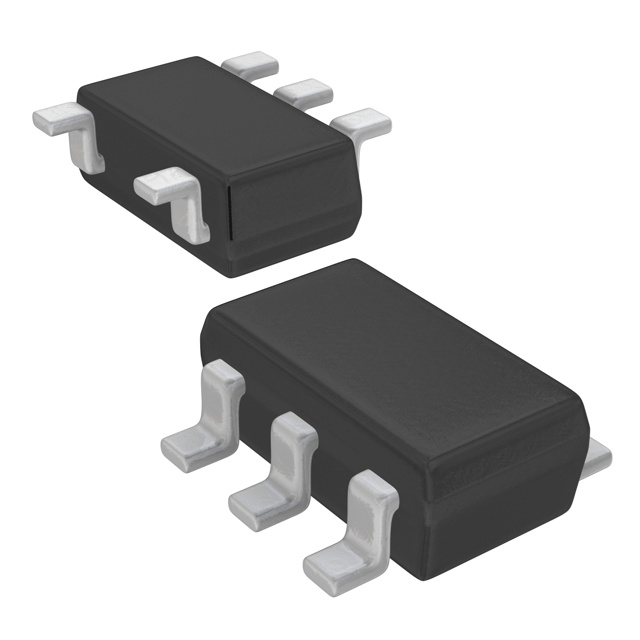
: SOT-25, USP-6C
* When using external components showing in the circuit below.
■TYPICAL PERFORMANCE
CHARACTERISTICS
XC9122D091 (100kHz, 15.0V)
L=47uH(CDRH5D28),SD:XB01SB04A2
CL=40uF(Ceramic),Tr:161A11A1
100
4.2V
Efficiency: EFFI(%)
■TYPICAL APPLICATION CIRCUIT
PWM/PFM
80
VIN=2.7V
60
3.2V
3.6V
PWM
40
20
0
0.1
1
10
100
Output Current: IOUT(mA)
1/17
�XC9120/XC9121/XC9122 Series
■PIN CONFIGURATION
EXT
GND
55
44
1
22
33
FB
VDD
CE
* The dissipation pad for the
USP-6C package should be
solder-plated in recommended
mount pattern and metal masking
so as to enhance mounting strength
and heat release. If the pad needs
to be connected to other pins, it
should be connected to the VDD pin
(Pin #2).
USP-6C (BOTTOM VIEW)
SOT-25 (TOP VIEW)
■PIN ASSIGNMENT
PIN NUMBER
PIN NAME
FUNCTION
6
FB
Output Voltage Setting Resistor Connection
2
VDD
Supply Voltage
CE
Chip Enable (Operates when "H" Level)
SOT-25
USP-6C
1
2
3
4
CE (/PWM)
PWM/PFM Switch*
4
3
GND
Ground
5
1
EXT
External Transistor Drive Connection
-
5
NC
No Connection
* The XC9122 series combines the CE pin and PWM/PFM switch pin.
■FUNCTION
XC9120/9121 Series
CE PIN
H
Operation
L
Shut-Down
XC9122 Series
CE/PWM PIN
H
More than VDD - 0.2 (V)
M
0.65 ~ VDD – 1.0 (V)
L
0 ~ 0.2 (V)
2/17
IC OPERATIONAL STATE
IC OPERATIONAL STATE
Operation (PWM control)
Operation (PWM/PFM automatic switching control
Shut-Down
�XC9120/XC9121/XC9122
Series
■ PRODUCT CLASSIFICATION
●Ordering Information
XC9120①②③④⑤⑥-⑦(*1): PWM Control
XC9121①②③④⑤⑥-⑦(*1): PWM/PFM Automatic Switching Control
XC9122①②③④⑤⑥-⑦(*1): PWM/PFM Externally Switching Control
DESIGNATOR
DESCRIPTION
SYMBOL
①
Type of DC/DC Controller
② ③
Output Voltage
D
09
④
Oscillation Frequency
1
B
: With current limiter
: No current limiter
: FB Voltage (ex. FB Voltage=0.9V→②=0, ③=9)
: 100kHz
: SOT-25
MR
MR-G
Packages
(*2)
Taping Type
⑤⑥-⑦
ER
: SOT-25 (Halogen & Antimony free)
: USP-6C
ER-G
(*1)
DESCRIPTION
: USP-6C (Halogen & Antimony free)
The “-G” suffix indicates that the products are Halogen and Antimony free as well as being fully EU RoHS
compliant.
(*2)
The device orientation is fixed in its embossed tape pocket. For reverse orientation, please contact your local
Torex sales office or representative. (Standard orientation: ⑤R-⑦, Reverse orientation: ⑤L-⑦)
■ BLOCK DIAGRAM
■ ABSOLUTE MAXIMUM RATINGS
Ta=25℃
PARAMETER
SYMBOL
RATINGS
UNIT
VDD Pin Voltage
VDD
-0.3 ~ 12.0
V
FB Pin Voltage
VFB
-0.3 ~ 12.0
V
CE Pin Voltage
VCE
-0.3 ~ 12.0
V
EXT Pin Voltage
VEXT
-0.3 ~ VDD + 0.3
V
EXT Pin Current
IEXT
±100
mA
Power Dissipation
SOT-25
USP-6C
Pd
250
120
mW
Operating Temperature Range
Topr
-40 ~ +85
℃
Storage Temperature Range
Tstg
-55 ~ +125
℃
* Voltage is all ground standardized.
3/17
�XC9120/XC9121/XC9122 Series
■ELECTRICAL CHARACTERISTICS
XC9120B091, XC9121B091, XC9122B091
XC9120D091, XC9121D091, XC9122D091
PARAMETER
SYMBOL
FB Voltage
(fOSC=100kHz)
CONDITIONS
Ta=25℃
MIN.
TYP.
MAX.
UNIT
CIRCUIT
VFB
0.882
0.900
0.918
V
④
Supply Voltage Range
(*1)
VDD
1.8
-
6.0
V
①
Output Voltage Setting
Range
VOUTSET
1.5
-
30.0
V
②
Operation Start Voltage
VST1
-
-
0.9
V
③
Oscillation Start Voltage
(*1)
VST2
-
-
0.8
V
④
Operation Hold Voltage
VHLD
-
-
0.7
V
③
Supply Voltage 1
IDD1
Same as VST2, VDD=3.0V
-
25
50
μA
④
Supply Voltage 2
IDD2
Same as IDD1, FB=1.2V
-
13
30
μA
④
Stand-by Current
ISTB
Same as IDD1, CE=0V
-
-
1.0
μA
⑤
Oscillation Frequency
fOSC
Same as IDD1
85
100
115
kHz
④
Maximum Duty Ratio
MAXDTY
Same as IDD1
89
93
96
%
④
PFM Duty Ratio
PFMDTY
No Load (XC9121B/D, XC9122B/D types)
24
32
40
%
⑥
150
250
400
mV
⑥
-
85
-
%
①
5.0
10.0
20.0
ms
①
Recommended circuit using 2SD1628,
VIN=VOUTSET×0.6, VDD=3.0V,
IOUT=1.0mA
Recommended circuit using 2SD1628
VOUT=3.3V, IOUT=1.0mA
No external components,
CE connected to VDD, Voltage applied,
FB=0V
Recommended circuit using 2SD1628
VOUT=3.3V, IOUT=1.0mA
Over Current Sense
Voltage (*2)
VLMT
Step input to FB
(Pulse width: 2.0μs or more)
EXT= Low level voltage
(XC9120/9122/9122B type)
Efficiency (*3)
EFFI
IOUT=10mA
Soft-Start Time
tSS
CE "H" Voltage
VCEH
Same as IDD1
0.65
-
-
V
⑤
CE "L" Voltage
VCEL
Same as IDD1
-
-
0.20
V
⑤
EXT "H" ON Resistance
REXTH
Same as IDD1, VEXT=VOUT-0.4V
-
24
36
Ω
④
EXT "L" ON Resistance
REXTL
Same as IDD1, VEXT=0.4V
-
16
24
Ω
④
PWM ‘H’ Voltage (*4)
VPWMH
IOUT=1mA
(XC9122B/D type)
VDD-0.2
-
-
V
①
PWM ‘L’ Voltage (*4)
VPWML
IOUT=1mA
(XC9122B/D type)
-
-
VDD-1.0
V
①
CE "H" Current
ICEH
Same as IDD2, CE=VDD
-
-
0.1
μA
⑤
CE "L" Current
ICEL
Same as IDD2, CE=0V
-
-
-0.1
μA
⑤
FB "H" Current
IFBH
Same as IDD2, FB=VDD
-
-
0.1
μA
⑤
FB "L" Current
IFBL
Same as IDD2, FB=0V
-
-
-0.1
μA
⑤
Test Conditions: Unless otherwise stated, CL: ceramic, recommended MOSFET should be connected.
When VOUT is set at 15V, VIN=VDD=3.6V.
NOTE:
*1: Although the IC starts step-up operations from a VDD=0.8V, the output voltage and oscillation frequency are stabilized at VDD>1.8V.
Therefore, a VDD of more than 1.8V is recommended when VDD is supplied from VIN or other power sources.
*2: The overcurrent limit circuit of this IC is designed to monitor the ripple voltage so please select your external components carefully to
prevent VLMT being reached under low temperature conditions as well as normal operating conditions. Following current limiter circuit
operation, which in turn causes the IC’s operations to stop, the IC resumes its operation with a toggle of the CE pin or by turning the power
supply back on.
*3: EFFI: {(output voltage) x (output current)} / {(input voltage) x (input current)} x 100
*4: The XC9122 series’ CE pin combines PWM/PFM external switch pin. In the operation state, PWM control becomes effective when the CE
pin is more than VDD-0.2V. When the CE pin is less than VDD-1.0V and more than VCEH, PWM/PFM automatic switching control becomes
effective with 32% duty.
4/17
�XC9120/XC9121/XC9122
Series
■ TYPICAL APPLICATION CIRCUIT
SD
RSENSE
CFB
VOUT
RFB1
RFB2
1
CL
5
Nch Power
MOS FET
CIN
VIN
2
3
RB
4
CB
CE
NPM Tr
When obtaining VDD from a source other than VIN (VOUT),
please insert a by-pass capacitor CDD between the VDD
pin and the GND pin in order to provide stable operations.
Please place CL and CIN as close as to the VOUT and VDD
pins respectively and also close to the GND pin.
Strengthen the wiring sufficiently.
RSENSE should be removed and shorted when the CL
capacitor except for ceramic or low ESR capacitor is
used.
Insert RB and CB when using a bipolar
NPN transistor.
5/17
�XC9120/XC9121/XC9122 Series
■ OPERATIONAL EXPLANATION
The XC9120/9121/9122 series consists of a reference voltage source, ramp wave circuit, error amplifier, PWM comparator,
phase compensation circuit, and current limiter circuit. The series ICs compare, using the error amplifier, the voltage of the
internal voltage reference source with the feedback voltage from the FB pin. Phase compensation is performed on the
resulting error amplifier output, to input a signal to the PWM comparator to determine the turn-on time during PWM operation.
The PWM comparator compares, in terms of voltage level, the signal from the error amplifier with the ramp wave from the
ramp wave circuit, and delivers the resulting output to the buffer driver circuit to cause the EXT pin to output a switching duty
cycle. This process is continuously performed to ensure stable output voltage.
Error amplifier is designed to monitor the output voltage, comparing the feedback voltage (FB) with the reference voltage
Vref. In response to feedback of a voltage lower than the reference voltage Vref, the output voltage of the error amp.
decreases.
The circuit generates the internal reference clock. The frequency is set to 100kHz (TYP.).
The ramp wave generator generates a saw-tooth waveform based on outputs from the OSC Generator.
The PWM comparator compares outputs from the error amp. and saw-tooth waveform. When the voltage from the error
amp’s output is low, the external switch will be set to ON.
The circuit generates PFM pulses.
The XC9122 series can switch PWM control and PWM/PFM switching control by external signal. The PWM/PFM automatic
switching control becomes effective when the voltage of the CE pin is less than VDD-1.0V, and the control switches between
PWM and PFM automatically depending on the load. The PWM/PFM control turns into the PFM control when threshold
voltage becomes lower then voltage of error amps. The PWM control becomes effective when the CE pin voltage is more
than VDD-0.2V. Noise is easily reduced with the PWM control since the switching frequency is fixed. Because of this, the
series gives the best control suitable for your application.
The reference voltage, Vref (FB pin voltage) =0.9V, is adjusted and fixed by laser trimming (for output voltage settings, please
refer to the output voltage setting.). Soft-start circuit protects against inrush current, when the power is switched on, and
also protects against voltage overshoot. It should be noted, however, that this circuit does not protect the load capacitor (CL)
form inrush current. With the Vref voltage limited and depending on the input to the error amps, the operation maintains a
balance between the two inputs of the error amps and controls the EXT pin’s ON time so that it does not increase more than
is necessary.
The function controls the operation and shutdown of the IC. When the voltage of the CE pin is 0.2V or less, the mode will be
disable, the channel’s operations will stop and the EXT pin will be kept at a low level (the external N-ch MOSFET will be
OFF). When the IC is in a state of disable, current consumption will be no more than 1.0μA. When the CE pin’s voltage is
0.65V or more, the mode will be enabled and operations will recommence.
The current limiter circuit of the XC9120 series is designed to monitor a ripple output voltage. Following current limiter
circuit operation, which in turn causes the IC’s operations to stop, the IC resumes its operation with a toggle of the CE pin or
by turning the power supply back on.
6/17
�XC9120/XC9121/XC9122
Series
■ OPERATIONAL EXPLANATION (Continued)
Output voltage can be set by adding external split resistors. Output voltage is determined by the following equation, based
on the values of RFB1 and RFB2. The sum of RFB1 and RFB2 should normally be 2MΩ.
VOUT = 0.9 x (RFB1 + RFB2) / RFB2
The value of CFB1, speed-up capacitor for phase compensation, should result in fzfb = 1/(2×π×CFB×RFB1) equal to
15kHz. Adjustments are required between 5kHz to 30kHz depending on the application, value of inductance (L), and value
of load capacitance (CL).
ex.) Output Voltage Setting
VOUT
RFB1
RFB2
(V)
(kΩ)
(kΩ)
390
12
30.0
270
10
25.0
470
22
20.0
510
27
18.0
CFB
(pF)
27
39
22
18
VOUT
(V)
15.0
10.0
7.0
3.3
RFB1
(kΩ)
470
150
150
150
RFB2
(kΩ)
30
15
22
56
CFB
(pF)
22
68
68
68
The circuit of the XC9120 series is organized by a specialized circuit, which reenacts negative feedback of both voltage and
current. Also by insertion of approximately 50mΩ of a low and inexpensive sense resistor as current sense, a high degree
of stability is possible even using a ceramic capacitor, a condition which used to be difficult to achieve. Compared to a
tantalum condenser, because the series can be operated in a very small capacity, it is suited to use of the ceramic capacitor,
which is cheap and small.
Tr
SD
L, CL
L
CL
RSENSE
CL
L
CL
RSENSE
: *When a MOSFET is used
XP161A1355PR (N-Channel Power MOSFET, TOREX)
Note: As the breakdown voltage of XP161A1355PR is 20V,
take care with the output voltage. With output
voltages over 17V, use the XP161A11A1PR with a
breakdown voltage of 30V.
VST1: XP161A1355PR=1.2V (MAX.)
XP161A11A1PR=2.5V (MAX.)
: XBS104S14R-G (Schottky Barrier Diode, TOREX)
:Please set up as follows according to an operating condition
or external components.
: 47μH (CDRH5D28, SUMIDA)
: 22μH (CDRH5D28, SUMIDA)
: 25V, 10μF (Ceramic type, TMK316BJ106KL, TAIYO YUDEN)
: 10V, 10μF (Ceramic type, LMK325BJ106ML, TAIYO YUDEN)
Use the formula below when step-up ratio and output current is
large.
CL = (CL standard value) x (IOUT (mA) / 100mA x VOUT / VIN)
: 50mΩ (fOSC = 100kHz)
*When a NPN Transistor is used:
2SD1628 (SANYO)
RB : 500Ω(Adjust with Tr’s HSE or load)
CB : 2200pF (Ceramic type)
CB