XC9128/XC9129 series is Discontinued.
XC9128/XC9129 Series
ETR0411-013
1A Driver Transistor Built-In, Step-Up DC/DC Converters
☆Green Operation Compatible
■GENERAL DESCRIPTION
The XC9128/XC9129 series are synchronous step-up DC/DC converters with a 0.2Ω (TYP.) N-channel driver transistor and
a synchronous 0.2Ω (TYP.) P-channel switching transistor built-in. A highly efficient and stable current can be supplied up to
1.0A by reducing ON resistance of the built-in transistors.
With a high switching frequency of 1.2MHz, a small inductor is selectable making the series ideally suited for applications
requiring low profile or space saving solutions. With the MODE pin, the series provides mode selection of PWM control or
PFM/PWM automatic switching control. In the PWM/PFM automatic switching mode, the series switches from PWM to PFM
to reduce switching loss when load current is small. When load current is large, the series switches automatically to the PWM
mode so that high efficiency is achievable over a wide range of load conditions. The series also provides small output ripple
from light to large loads by using the built-in circuit which enables the smooth transition between PWM and PFM.
With a adaptor enable function of the XC9128 series, when a voltage higher than the input voltage is applied to the output,
the input and the output become isolated making it possible for the IC to work in parallel with the likes of an AC adaptor.
■ FEATURES
■APPLICATIONS
●Digital audio equipment
High Efficiency, Large Current Step-Up Converter
: 150mA@VOUT=3.3V, VIN=0.9V
Output Current
500mA@VOUT=3.3V, VIN=1.8V
Input Voltage Range
: 0.8V ~ 6.0V
: 1.8V ~ 5.3V (Externally set)
Output Voltage Setting
Set up freely with a reference voltage
Range
supply of 0.45V (±0.010V) & external
components
: 1.2MHz
Oscillation Frequency
(Fixed oscillation frequency accuracy ±15%)
Input Current
: 1.0A
Maximum Current Limit
: 1.2A (MIN.), 2.0A (MAX.)
●Digital still cameras / Camcorders
●Computer Mouses
●Multi-function power supplies
: PWM, PWM/PFM control
externally selectable
High Speed
:100mV @ VOUT=3.3V,
Transient Response
VIN=1.8V, IOUT=10mA→100mA
: Thermal shutdown
Protection Circuits
Integral latch method (Over current limit)
Soft-Start Time
: 5ms (TYP.) internally set
Ceramic Capacitor Compatible
Adaptor Enable Function (XC9128 series)
Flag Output (XC9128 series) : Open-drain output
Operating Ambient Temperature : - 40 ~ 85℃
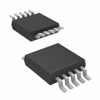
Packages
: MSOP-10, USP-10B
Environmentally Friendly
: EU RoHS Compliant, Pb Free
Control
■TYPICAL PERFORMANCE
CHARACTERISTICS
■TYPICAL APPLICATION CIRCUIT
●Efficiency vs. Output Current
XC9128B45CD
VOUT
10
2
Lx
MODE
9
3
BAT
FB
8
4
EN
MODE
VIN
L
EN
FO
5
FO
AGND
AEN/
100
VOUT
PGND
1
90
CFB
RFB1
7
6
RFB2
CL
(ceramic)
Efficiency: EFFI (%)
CIN
L=4.7μH(LTF5022-LC),CL =30μF(LMK212BJ106KG ×3)
VOUT=3.3V,VEN=6V,VFO =OPEN,VAEN/ =0V
RFB1 =270kΩ,RFB2 =43kΩ,CFB=12pF,CIN=10μF
80
70
1.8V
60
3.0V
50
40
30
20
PWM/PFM (VMODE=0V)
PWM (VMODE=VOUT)
10
0
0.1
1
10
100
1000
Output Current: I OUT (mA)
1/28
�XC9128/XC9129 series
is Discontinued.
XC9128/XC9129 Series
■BLOCK DIAGRAM
●XC9128 Series
AGND
VOUT
Error Amp.
FB
Phase
Compensation
PWM
comparator
Current Sense,
Limit, PFM
Lx
PWM/PFM
Controller, Logic
AEN/
EN
Vref with
Soft Start
RAMP Wave
Generator
PGND
OSC
MODE
MODE
EN,
Thermal Shutdown
BAT
●XC9129 Series
The XC9129 series does not have AEN/ pin and FO pin.
2/28
Buffer
Driver
Current Limit,
Thermal,
Soft Start,
EN
FO
�XC9128/XC9129
XC9128/XC9129 series is Discontinued.
Series
■PRODUCT CLASSIFICATION
●Ordering Information
XC9128①②③④⑤⑥-⑦
・・・・Adaptor Chip Enable Pin and Flag Output Pin are added
(*1)
DESIGNATOR
ITEM
①
Integral Protection
②③
Reference Voltage
④
Oscillation Frequency
Packages
(Order Unit)
⑤⑥-⑦(*1)
XC9129①②③④⑤⑥-⑦
(*1)
SYMBOL
DESCRIPTION
B
With integral protection
D
Without integral protection
45
Fixed reference voltage 0.45V
②=4, ③=5
C
1.2MHz
AR
MSOP-10 (1,000pcs/Reel)
AR-G
MSOP-10 (1,000pcs/Reel)
DR
USP-10B (3,000pcs/Reel)
DR-G
USP-10B (3,000pcs/Reel)
・・・・Adaptor Chip Enable Pin and Flag Output Pin are not added
DESIGNATOR
ITEM
SYMBOL
①
Integral Protection
D
Without integral protection
②③
Reference Voltage
45
Fixed reference voltage 0.45V
②=4, ③=5
④
Oscillation Frequency
C
1.2MHz
⑤⑥-⑦(*1)
Package
(Order Unit)
DR
USP-10B (3,000pcs/Reel)
DR-G
USP-10B (3,000pcs/Reel)
(*1)
DESCRIPTION
The “-G” suffix denotes Halogen and Antimony free as well as being fully EU RoHS compliant.
3/28
�XC9128/XC9129 series
is Discontinued.
XC9128/XC9129 Series
■PIN CONFIGURATION
10 VOUT
10 VOUT
PGND 1
PGND
1
Lx 2Lx 2
8 FB
8 FB
EN EN 4
4
7 AGND
7 AGND
FO FO 5
5
6 AEN/
6 AEN/
6 6 AEN/
AEN/
EN
EN 4 4
7 7 AGND
AGND
BAT
BAT 3 3
9 MODE
9 MODE
BAT 3
BAT
3
FO
FO 5 5
8 8 FB
FB
Lx
Lx 2 2
9 9 MODE
MODE
PGND
PGND 1 1
1010VOUT
VOUT
USP-10B
USP-10B
( BOTTOM
VIEW )
(BOTTOM VIEW)
MSOP-10
XC9128 Series
MSOP-10
(TOP VIEW)
( TOP VIEW )
FO
NC 5 5
6 6 AEN/
NC
EN
EN 4 4
7 7 AGND
AGND
BAT
3
BAT 3
8 8 FB
FB
Lx
Lx 2 2
9 9 MODE
MODE
PGND
PGND 1 1
1010VOUT
VOUT
USP-10B
USP-10B
( BOTTOM
VIEW )
(BOTTOM VIEW)
XC9129 Series
■PIN ASSIGNMENT
MSOP-10*
1
2
3
4
5
6
7
8
9
10
-
PIN NUMBER
USP-10B*
(XC9128)
USP-10B*
(XC9129)
PIN NAME
FUNCTION
1
2
3
4
5
6
7
8
9
10
-
1
2
3
4
7
8
9
10
5, 6
PGND
Lx
BAT
EN
FO
AEN/
AGND
FB
MODE
VOUT
NC
Power Ground
Output of Internal Power Switch
Battery Input
Chip Enable
Flag Output
Adaptor Enable
Analog Ground
Output Voltage Monitor
Mode Switch
Output Voltage
No Connection
* For MSOP-10 and USP-10B packages, please short the GND pins (pins 1 and 7).
* The dissipation pad for the USP-10B package should be solder-plated following the recommended mount pattern and metal masking
so as to enhance mounting strength and heat release. If the pad needs to be connected to other pins, it should be connected to the
Ground pins (pins 1 and 7).
4/28
�XC9128/XC9129
XC9128/XC9129 series is Discontinued.
Series
■FUNCTION CHART
1. EN, AEN/ Pin Function
●XC9128 Series
EN PIN
AEN/ PIN
FB PIN VOLTAGE
IC OPERATIONAL STATE
SOFT-START FUNCTION
Operation
Available
Operation
Available
Operation
Not Available
L→H
L
-
H
H→L
H
H→L
Lower than 0.45×0.8V
Higher than
0.45×0.95V
H
H
-
Step-Up Operation ShutDown
-
L
L
-
Disable
-
L
H
-
Disable
-
* Do not leave the EN and AEN/ Pins open.
●XC9129 Series
EN PIN
IC OPERATIONAL STATE
H
Operation
L
Disable
* Do not leave the EN Pin open.
2. MODE Pin Function
●XC9128/XC9129 Series
MODE PIN
H
L
FUNCTION
PWM Control
PWM/PFM Automatic Switching Control
* Do not leave the MODE Pin open.
5/28
�XC9128/XC9129 series
is Discontinued.
XC9128/XC9129 Series
■ABSOLUTE MAXIMUM RATINGS
PARAMETER
SYMBOL
RATINGS
UNITS
VOUT Pin Voltage
VOUT
-0.3 ~ 6.5
V
AEN/ Pin Voltage
(*2)
FO Pin Voltage (*2)
VAEN/
-0.3 ~ 6.5
V
VFO
-0.3 ~ 6.5
V
mA
FO Pin Current (*2)
IFO
10
FB Pin Voltage
VFB
-0.3 ~ 6.5
V
BAT Pin Voltage
VBAT
-0.3 ~ 6.5
V
MODE Pin Voltage
VMODE
-0.3 ~ 6.5
V
EN Pin Voltage
VEN
-0.3 ~ 6.5
V
LX Pin Voltage
VLx
-0.3 ~ VOUT + 0.3
V
LX Pin Current
ILx
2000
mA
Power Dissipation
(Ta=25℃)
350
MSOP-10
Pd
USP-10B
500 (40mm x 40mm Standard board) (*1)
150
500 (40mm x 40mm Standard board) (*1)
Operating Ambient Temperature
Topr
-40 ~ 85
℃
Storage Temperature
Tstg
-55 ~ 125
℃
AGND, PGND is the standard voltage for all of voltages.
(*1)
This power dissipation figure shown is PCB mounted and is for reference only.
(*2)
The XC9129 series does not have AEN/ pin and FO pin. These pins are available only in the XC9128 series.
The mounting condition is please refer to PACKAGING INFORMATION.
6/28
mW
�XC9128/XC9129
XC9128/XC9129 series is Discontinued.
Series
■ELECTRICAL CHARACTERISTICS
XC9128/XC9129 Series
Ta=25℃
PARAMETER
SYMBOL
CONDITIONS
MIN.
TYP.
MAX.
UNITS
CIRCUIT
Input Voltage
VIN
-
-
-
6.0
V
-
0.44
0.45
0.46
V
④
1.8
-
5.3
V
①
-
-
0.8
V
①
-
-
0.9 (*1)
V
①
-
0.8
-
V
①
FB Voltage
VFB
Output Voltage Setting Range
VOUTSET
Operation Start Voltage
VST1
Oscillation Start Voltage
VST2
Operation Hold Voltage
VHLD
Supply Current 1
IDD1
Supply Current 2 (XC9128)
Supply Current 2 (XC9129)
IDD2
VOUT=VIN=3.3V, VFO=0V (*8)
Voltage to start oscillation during
VFB= 0.46V → 0.44V
Connect to external components,
RL=1kΩ
Connect to external components,
RL=33Ω
Voltage to start oscillation during
VIN=0V → 1V, RL=1kΩ
Connect to external components, RL=1kΩ
VIN = VOUT =3.3V, VFB=0.45V×0.9
VIN = VOUT =3.3V
VFB=0.45V×1.1 (Oscillation stop),
VMODE=0V
VIN =3.3V, VOUT =1.8V, VEN=0V
VIN = VOUT =3.3V, VEN=0V
VIN = VOUT =3.3V, VFO=0V (*8),
VFB=0.45V×0.9
VIN = VOUT =3.3V, VFO=0V (*8),
VFB=0.45V×0.9
VIN = VOUT =3.3V, VFO=0V (*8),
VFB=0.45V×1.1
Connect to external components,
VMODE=0V, RL=330Ω
Connect to external components,
RL=33Ω
VIN=VLx=VOUT+50mV,
VFB=0.45V×1.1 (*3)
-
0.7
-
V
①
-
3
6
mA
②
-
30
80
-
28
78
μA
②
-
2
2
10
10
μA
μA
③
②
1.02
1.20
1.38
MHz
④
85
92
96
%
④
-
-
0
%
④
-
250
400
mA
①
-
93
-
%
①
-
0.20
0.35 (*1)
Ω
⑤
Input Pin Current
Stand-by Current
IBAT
ISTB
Oscillation Frequency
fOSC
Maximum Duty Cycle
MAXDTY
Minimum Duty Cycle
MINDTY
PFM Switching Current
IPFM
Efficiency (*2)
EFFI
LX SW "Pch" ON Resistance
RLxP
LX SW "Nch" ON Resistance
RLxN
VIN=VOUT=3.3V, Lx =50mV (*4)
-
0.20 (*1)
0.35 (*1)
Ω
⑦
LX Leak Current
ILXL
VIN=VOUT= VLX, VFB=0V
-
1
-
μA
⑤
Current Limit
ILIM
VOUT>2.5V
Time to stop oscillation during
RL=33Ω → 3.3Ω, VFO=L → H
Time to stop oscillation during
RL=33Ω → 3.3Ω
Time to start oscillation during VEN=0V
→ VIN at VIN = VOUT =3.3V, VFO=0V,
VFB=0.45V×0.95
VIN = VOUT =3.3V, VFO=0V,
VFB=0.45V×0.95
Time to start oscillation during
VAEN/=VIN→0V.
VIN = VOUT =3.3V, VFO=0V,
VFB=0.45V×0.8
Time to start oscillation during
VAEN/=VIN→0V
1.2
1.5
2.0
A
①
-
3.5
-
ms
①
1.7
5.3
10.5
ms
④
-
0.02
0.04
ms
④
1.7
5.3
10.5
ms
④
(*5)
Integral Latch Time (XC9128) (*6)
Integral Latch Time (XC9129) (*6)
tLAT
Soft-Start Time 1
tSS1
Soft-Start Time 2 (*7)
tSS2
Soft-Start Time 3 (*7)
tSS3
Thermal Shutdown
Temperature
Hysteresis Width
TTSD
-
-
150
-
℃
-
THYS
VIN =3.3V
Voltage to stop oscillation during
VOUT=1.56V→1.3V
VIN =VOUT=3.3V, VFO=0.25V
VIN = VOUT =3.3V, VEN=0V ,VFO=1V
-
20
-
℃
-
1.3
1.48
1.56
V
⑥
1.3
-
1.7
0
2.2
1
mA
μA
④
④
Output Voltage Drop
Protection (*6)
VLVP
FO Output Current (*7)
FO Leakage Current (*7)
IFO_OUT
IFO_Leak
7/28
�XC9128/XC9129 series
is Discontinued.
XC9128/XC9129 Series
■ELECTRICAL CHARACTERISTICS (Continued)
●XC9128/XC9129 Series (Continued)
PARAMETER
EN "H" Voltage
Ta=25℃
UNIT CIRCUIT
S
SYMBOL
CONDITIONS
MIN.
TYP.
MAX
VENH
VIN =VOUT=3.3V, VFO=0V (*8)
Voltage to start oscillation during
VFB=0.45V×0.9, VEN= 0.2V→0.65V
0.65
-
6.0
V
④
AGND
-
0.2
V
④
VIN = VOUT =3.3V, VFO=0V (*8)
Voltage to stop oscillation during
VFB=0.45V×0.9,
VEN= 0.65V→0.20V
EN "L" Voltage
VENL
MODE "H" Voltage
VMODEH
RL =330Ω, Voltage operates at PWM control
0.65
-
6.0
V
①
MODE "L" Voltage
VMODEL
RL =330Ω, Voltage operates at PFM control
AGND
-
0.2
V
①
AEN/ Voltage (*7)
VAEN/
VIN = VOUT =3.3V, VFO=0V
Voltage to start oscillation during VAEN/= 0.9V→0.7V
0.7
0.8
0.9
V
④
EN "H" Current
IENH
VIN=VOUT=VFB=VEN=6.0V
-
-
0.1
μA
②
EN "L" Current
IENL
VIN=VOUT=VFB=6.0V, VEN=0V
-0.1
-
-
μA
②
MODE "H" Current
IMODEH
VIN=VOUT=VFB=VMODE=6.0V
-
-
0.1
μA
②
MODE "L" Current
IMODEL
VIN=VOUT=VFB=6.0V, VMODE=0V
-0.1
-
-
μA
②
AEN/ "H" Current (*7)
IAEN/H
VIN=VOUT=VFB=VAEN/=6.0V
-
-
0.1
μA
②
AEN/ "L" Current (*7)
IAEN/L
VIN=VOUT=6.0V, VEN=0V, VAEN/=0V
-0.1
-
-
μA
②
FB "H" Current
IFBH
VIN=VOUT=VFB=6.0V
-
-
0.1
μA
②
FB "L" Current
IFBL
VIN=VOUT=6.0V, VFB=0V
-0.1
-
-
μA
②
Test Conditions:
For the Circuit No.1, unless otherwise stated, VIN=1.8V, VEN=VMODE=VFO=3.3V, VAEN/=0V
(*8)
For the Circuit No.2, unless otherwise stated, VIN=1.8V, VFB =0V, VEN=VMODE=3.3V, VAEN/=0V
(*8)
For the Circuit No.3, unless otherwise stated, VIN=1.8V, VOUT=VEN=VMODE=3.3V, FB=0V
For the Circuit No.4, unless otherwise stated, VIN=1.8V, VFB=0V, VEN=VMODE=Vpull=VFO=3.3V, VAEN/ =0V
For the Circuit No.5, unless otherwise stated, VIN=3.3V, VAEN/=0V
(*8)
(*8)
For the Circuit No.6, unless otherwise stated, VEN=VMODE=Vpull=VFO=3.3V, VFB=0V
(*8)
For the Circuit No.7, unless otherwise stated, VEN=VMODE=3.3V
External Components:
For the Circuit No.1, RFB1=270kΩ, RFB2=43kΩ, CFB=12pF, L=4.7μH(LTF5022 TDK), CL1=22μF(ceramic),
CL2=10μF(ceramic), CIN=10μF(ceramic)
For the Circuit No.2,3, CIN=1μF(ceramic)
For the Circuit No.4,6, CIN=1μF(ceramic), Rpull=300Ω
For the Circuit No.5, CIN=1μF(ceramic), COUT=1μF(ceramic)
For the Circuit No.7, CIN=1μF(ceramic), COUT=1μF(ceramic), SBD =XBS304S17(TOREX), Rpull=0.5Ω
1 : Designed value
*
2 : Efficiency ={(output voltage) X (output current)} ÷ {(input voltage) X (input current)} X 100
*
3 : LX SW "Pch" ON resistance=(VLx-VOUT pin test voltage)÷100mA
*
4 : Testing method of LX SW "Nch" ON resistance is stated at test circuits.
*
5 : Current flowing through the Nch driver transistor is limited.
*
6 : The XC9128D/XC9129D type does not have integral latch protection and VLVP function.
*
This is only available with the XC9128B type.
7 : The XC9129 series does not have FO and AEN/ pins. These pins are only available in the XC9128 series.
*
8 : The XC9129 series does not have FO and AEN/ pins. The AEN/FO functions are only effective for the test of the XC9128 series.
*
8/28
�XC9128/XC9129
XC9128/XC9129 series is Discontinued.
Series
■TYPICAL APPLICATION CIRCUIT
CL1
CIN
1
PGND
VOUT
10
2
Lx
MODE
9
3
BAT
FB
8
4
EN
AGND
7
5
FO
AEN/
6
VIN
L
EN
FO
VOUT
MODE
CL2
CFB
RFB1
RFB2
Output voltage can be set by adding external split resistors. Output voltage is determined by the following equation,
based on the values of RFB1 and RFB2. The sum of RFB1 and RFB2 should normally be 500kΩ or less.
VOUT=0.45 × (RFB1 + RFB2) / RFB2
The value of CFB, speed-up capacitor for phase compensation, should be fZFB = 1 / (2 x π x CFB1 x RFB1) which is in
the range of 10 kHz to 60 kHz. Adjustments are depending on application, inductance (L), load capacitance (CL) and
dropout voltage.
[Example of calculation]
When RFB1=270kΩ, RFB2=43kΩ,
VOUT1 = 0.45 × (270k+43k ) / 43k = 3.276V
VOUT (V)
RFB1 (kΩ)
RFB2 (kΩ)
CFB (pF)
1.8
2.5
3.3
5.0
300
270
270
180
100
59
43
17.8
10
12
12
15
[External Components]
1.2MHz:
L : 4.7μH (LTF5022-4R7-LC TDK)
: 4.7μH (CDRH4D28C-4R7N SUMIDA)
CL1 : 22μF (ceramic)
CL2 : 10μF (ceramic)
CIN : 10μF (ceramic)
* CL1 should be selected in 10μF or higher.
Capacitance CL1 + CL2 is recommended 30μF or higher. (Ceramic capacitor compatible)
If CL1 is lower than 10μF, operation may be unstable.
In case of the usage CL1 + CL2 <30μF, output ripple may increase so that we recommend that you fully check
actual performance on the board.
* If using Tantalum or Electrolytic capacitors please be aware that ripple voltage will be higher due to the larger
ESR (Equivalent Series Resistance) values of those types of capacitors. Please also note that the IC’s
operation may become unstable with such capacitors so we recommend that you fully check actual
performance.
9/28
�XC9128/XC9129 series
is Discontinued.
XC9128/XC9129 Series
■OPERATIONAL EXPLANATION
The XC9128/XC9129 series consists of a reference voltage source, ramp wave circuit, error amplifier, PWM comparator,
phase compensation circuit, N-channel driver transistor, P-channel synchronous rectification switching transistor and current
limiter circuit. The error amplifier compares the internal reference voltage with the FB pin feed back voltage via resistors RFB1
and RFB2. Phase compensation is performed on the resulting error amplifier output, to input a signal to the PWM comparator
to determine the turn-on time of the N-channel driver transistor during PWM operation. The PWM comparator compares, in
terms of voltage level, the signal from the error amplifier with the ramp wave from the ramp wave circuit, and delivers the
resulting output to the buffer driver circuit to cause the Lx pin to output a switching duty cycle. This process is continuously
performed to ensure stable output voltage. The current feedback circuit monitors the N-channel driver transistor’s turn-on
current for each switching operation, and modulates the error amplifier output signal to provide multiple feedback signals.
This enables a stable feedback loop even when a low ESR capacitor, such as a ceramic capacitor, is used, ensuring stable
output voltage.
The source provides the reference voltage to ensure stable output of the DC/DC converter.
The ramp wave circuit determines switching frequency. The frequency is fixed internally at 1.2MHz. The Clock generated is
used to produce ramp waveforms needed for PWM operation, and to synchronize all the internal circuits.
The error amplifier is designed to monitor output voltage. The amplifier compares the reference voltage with the feedback
voltage divided by the internal resistors (RFB1 and RFB2). When the FB pin is lower than the reference voltage, output voltage
of the error amplifier increases. The gain and frequency characteristics of the error amplifier are optimized internally.
< Maximum Current Limit>
The current limiter circuit monitors the maximum current flowing through the N-channel driver transistor connected to the Lx
pin, and features a combination of the current limit and latch function.
When the driver current is greater than a specific level (equivalent to peak coil current), the maximum current limit
function starts to operate and the pulses from the Lx pin turn off the N-channel driver transistor at any given time.
When the driver transistor is turned off, the limiter circuit is then released from the maximum current limit detection state.
At the next pulse, the driver transistor is turned on. However, the transistor is immediately turned off in the case of an
over current state.
When the over current state is eliminated, the IC resumes its normal operation.
The XC9128B type waits for the over current state to end by repeating the steps through . If an over current state continues
for several ms and the above three steps are repeatedly performed, the IC performs the function of latching the OFF state of the
N-channel driver transistor, and goes into operation suspension mode. After being put into suspension mode, the IC can resume
operation by turning itself off once and then re-starting via the EN pin, or by restoring power to the V IN pin.
The XC9128D/XC9129D type does not have this latch function, so operation steps through repeat until the over current
state ends.
Integral latch time may be released from a over current detection state because of the noise. Depending on the state of a
substrate, it may result in the case where the latch time may become longer or the operation may not be latched. Please locate
an input capacitor as close as possible.
Limit
< Circuit No.3 >
A
A
CIN
Lx
VOUT
BAT
MODE
EN
VIN
A
FB
FO
AEN/
VEN
PGND
A
VAEN/
VMODE
VOUT
BAT
MODE
EN
CIN
FB
FB
VOUT
VIN
VMODE
FO
AEN/
VFB
VEN
PGND
AGND
CIN
※ External Components
A
A
Lx
: 1uF (ceramic)
AGND
※ External Components
< Circuit No.4 >
CIN
: 1uF (ceramic)
Wave Form Measure Point
Rpull
Lx
VOUT
BAT
MODE
Lx
VOUT
BAT
MODE
Vpull
A
A
VIN
CIN
VEN
EN
FB
FO
AEN/
PGND
AGND
VMODE
CIN
※ External Components
FB
FO
AEN/
PGND
AGND
VLx
FB
A
VFO
EN
COUT
VAEN/
VOUT
VFB
VIN
VAEN/
※ External Components
CIN
: 1uF (ceramic)
Rpull : 300Ω
CIN : 1uF (ceramic)
COUT : 1uF (ceramic)
Wave Form Measure Point
Wave Form Measure Point
Rpull
Lx
VIN
VOUT
SBD
Vpull
A
BAT
EN
CIN
VEN
A
VFO
FB
PGND
※ External Components
V
AEN/
CLX
BAT
MODE
CIN
EN
FB
FO
AEN/
COUT
VIN
VEN
AGND
CIN : 1uF (ceramic)
Rpull : 300Ω
VOUT
Vpull
VOUT
FB
Lx
Rpull
MODE
VMODE
FO
V1
PGND
※ External Components
VOUT
VMODE
AGND
CIN
: 1uF (ceramic)
COUT : 1uF (ceramic)
SBD : XBS304S17(TOREX)
Rpull : 0.5Ω
Measurement method for ON resistance of the Lx switch
Using the layout of circuit No.7 above, set the LX pin voltage to 50mV by adjusting the Vpull voltage whilst the Nch driver
transistor is turned on. Then, measure the voltage difference between both ends of Rpull. ON Resistance is calculated by using
the following formula:
RLXN=0.05 ÷ ((V1 – 0.05) ÷ 0.5)
where V1 is a voltage between SBD and Rpull. LX pin voltage and V1 are measured by an oscilloscope.
*1: The XC9129 series does not have the AEN/ pin and the FO pin. When the XC9129 series is measured, the FO and AEN pins
are not effective in the above mentioned test circuits, they are NC.
14/28
�XC9128/XC9129
XC9128/XC9129 series is Discontinued.
Series
■TYPICAL PERFORMANCE CHARACTERISTICS
(1) Efficiency vs. Output Current
XC9128 (VOUT=3.3V)
L=4.7μH(LTF5022-LC),CL =30μF(LMK212BJ106KG ×3)
VEN=6V,VFO =OPEN,VAEN/ =0V
RFB1 =270kΩ,RFB2 =43kΩ,CFB=12pF,CIN=10μF
100
90
80
80
70
3.0V
60
50
1.8V
40
30
V IN=0.8V
20
0
0.1
1
10
100
4.2V
70
60
3.0V
50
1.8V
40
30
V IN=0.8V
20
PWM/PFM(VMODE=0V)
PWM(VMODE=VOUT)
10
L=4.7μH(LTF5022-LC),CL =30μF(LMK212BJ106KG ×3)
VEN=6V,VFO =OPEN,VAEN/ =0V
RFB1 =180kΩ,RFB2 =18kΩ,CFB=15pF,CIN=10μF
100
90
Efficiency: EFFI(%)
Efficiency: EFFI (%)
XC9128 (VOUT=5.0V)
PWM/PFM(VMODE=0V)
PWM(VMODE=VOUT)
10
0
1000
0.1
1
10
100
1000
Output Current: I OUT (mA)
Output Current: I OUT (mA)
XC9128 (VOUT=1.8V)
L=4.7μH(LTF5022-LC),CL =20μF(LMK212BJ106KG ×2)
VEN=6V,VFO =OPEN,VAEN/ =0V
RFB1 =300kΩ,RFB2 =100kΩ,CFB=10pF,CIN=10μF
100
Efficiency: EFFI (%)
90
80
70
1.5V
60
1.2V
50
40
V IN=0.8V
30
20
PWM/PFM(VMODE=0V)
PWM(VMODE=VOUT)
10
0
0.1
1
10
100
1000
Output Current: I OUT (mA)
15/28
�XC9128/XC9129 series
is Discontinued.
XC9128/XC9129 Series
■TYPICAL PERFORMANCE CHARACTERISTICS (Continued)
(2) Output Voltage vs. Output Current
V M O D E = 0 V (P W M / P FM ),VEN=6V,VFO =OPEN,VAEN/ =0V
L=4.7μH(LTF5022-LC),RFB1 =270kΩ,RFB2 =43kΩ
L=4.7μH(LTF5022-LC),RFB1 =270kΩ,RFB2 =43kΩ
CL =30μF(LMK212BJ106KG ×3),CFB=12pF,CIN=10μF
CL =30μF(LMK212BJ106KG ×3),CFB=12pF,CIN=10μF
3.5
Output Voltage : V OUT (V)
3.5
Output Voltage: V OUT (V)
V M O D E = V O U T (P W M ),VEN=6V,VFO =OPEN,VAEN/ =0V
3.4
V IN=0.8V,1.8V,3.0V
3.3
3.2
3.1
3.4
3.3
3.2
3.1
0.1
1
10
100
1000
0.1
Output Current: I OUT (mA)
L=4.7μH(LTF5022-LC),RFB1 =180kΩ,RFB2 =18kΩ
CL =30μF(LMK212BJ106KG ×3),CFB=15pF,CIN=10μF
5.1
V IN=0.8V,1.8V,3.3V,4.2V
5
4.9
100
1000
5.1
V IN=0.8V,1.8V,3.3V,4.2V
5
4.9
4.8
4.8
0.1
1
10
100
1000
0.1
Output Current: I OUT (mA)
10
100
1000
V IN=0.8V,1.2V,1.5V
1.8
1.7
V M O D E = 0 V (P W M / P FM ),VEN=6V,VFO =OPEN,VAEN/ =0V
L=4.7μH(LTF5022-LC),RFB1 =300kΩ,RFB2 =100kΩ
CL =20μF(LMK212BJ106KG ×2),CFB=10pF,CIN=10μF
2.0
Output Voltage: V OUT (V)
1.9
1
Output Current: I OUT (mA)
V M O D E = V O U T (P W M ),VEN=6V,VFO =OPEN,VAEN/ =0V
L=4.7μH(LTF5022-LC),RFB1 =300kΩ,RFB2 =100kΩ
CL =20μF(LMK212BJ106KG ×2),CFB=10pF,CIN=10μF
2.0
Output Voltage: V OUT (V)
10
V M O D E = 0 V (P W M / P FM ),VEN=6V,VFO =OPEN,VAEN/ =0V
L=4.7μH(LTF5022-LC),RFB1 =180kΩ,RFB2 =18kΩ
CL =30μF(LMK212BJ106KG ×3),CFB=15pF,CIN=10μF
5.2
Output Voltage: V OUT (V)
Output Voltage: V OUT (V)
5.2
1
Output Current: I OUT (mA)
V M O D E = V O U T (P W M ),VEN=6V,VFO =OPEN,VAEN/ =0V
1.9
V IN=0.8V,1.2V,1.5V
1.8
1.7
1.6
1.6
0.1
1
10
100
Output Current: I OUT (mA)
16/28
V IN=0.8V,1.8V
3.0V
1000
0.1
1
10
100
Output Current: I OUT (mA)
1000
�XC9128/XC9129
XC9128/XC9129 series is Discontinued.
Series
■TYPICAL PERFORMANCE CHARACTERISTICS (Continued)
(3) Ripple Voltage vs. Output Current
XC9128 (VOUT=3.3V)
XC9128 (VOUT=3.3V)
L= 4 . 7 μ H (LT F5 0 2 2 - LC), C L = 3 0 μ F(LM K 2 1 2 B J1 0 6 K G × 3 )
VEN=6V,VFO =OPEN,VAEN/ =0V
RFB1 =270kΩ,RFB2 =43kΩ,CFB=12pF,CIN=10μF
PWM/PFM(VMODE=0V)
PWM(VMODE=VOUT)
80
V IN=0.8V,1.8V,3.0V
60
0.8V
1.8V
3.0V
40
20
100
Ripple Voltage: Vr (mVp-p)
Ripple Voltage: Vr (mVp-p)
100
L= 4 . 7 μ H (LT F5 0 2 2 - LC), C L = 2 0 μ F(LM K 2 1 2 B J1 0 6 K G × 2 )
VEN=6V,VFO =OPEN,VAEN/ =0V
RFB1 =270kΩ,RFB2 =43kΩ,CFB=12pF,CIN=10μF
0
PWM/PFM(VMODE=0V)
PWM(VMODE=VOUT)
80
V IN=0.8V,1.8V,3.0V
60
40
20
1
10
100
1000
0.1
1
V IN=0.8V,1.8V,3.0V
60
0.8V
3.0V
1.8V
1000
40
20
L= 1 0 μ H (LT F5 0 2 2 - LC), C L = 2 0 μ F(LM K 2 1 2 B J1 0 6 K G × 2 )
VEN=6V,VFO =OPEN,VAEN/ =0V
RFB1 =270kΩ,RFB2 =43kΩ,CFB=12pF,CIN=10μF
100
Ripple Voltage: Vr (mVp-p)
PWM/PFM(VMODE=0V)
PWM(VMODE=VOUT)
80
100
XC9128 (VOUT=3.3V)
XC9128 (VOUT=3.3V)
L= 1 0 μ H (LT F5 0 2 2 - LC), C L = 3 0 μ F(LM K 2 1 2 B J1 0 6 K G × 3 )
VEN=6V,VFO =OPEN,VAEN/ =0V
RFB1 =270kΩ,RFB2 =43kΩ,CFB=12pF,CIN=10μF
100
10
Output Current: I OUT (mA)
Output Current: I OUT (mA)
Ripple Voltage: Vr (mVp-p)
3.0V
0
0.1
80
V IN=0.8V,1.8V,3.0V
PWM/PFM(VMODE=0V)
PWM(VMODE=VOUT)
3.0V
60
0.8V
1.8V
40
20
0
0
0.1
1
10
100
0.1
1000
1
V IN=0.8V,1.8V,3.3V,3.6V
60
0.8V
1.8V
3.3V
1000
3.6V
40
20
L= 4 . 7 μ H (LT F5 0 2 2 - LC), C L = 2 0 μ F(LM K 2 1 2 B J1 0 6 K G × 2 )
VEN=6V,VFO =OPEN,VAEN/ =0V
RFB1 =300kΩ,RFB2 =100kΩ,CFB=10pF,CIN=10μF
100
Ripple Voltage: Vr (mVp-p)
PWM/PFM(VMODE=0V)
PWM(VMODE=VOUT)
80
100
XC9128 (VOUT=1.8V)
XC9128 (VOUT=5.0V)
L= 4 . 7 μ H (LT F5 0 2 2 - LC), C L = 3 0 μ F(LM K 2 1 2 B J1 0 6 K G × 3 )
VEN=6V,VFO =OPEN,VAEN/ =0V
RFB1 =180kΩ,RFB2 =18kΩ,CFB=15pF,CIN=10μF
100
10
Output Current: I OUT (mA)
Output Current: I OUT (mA)
Ripple Voltage: Vr (mVp-p)
1.8V
0.8V
80
PWM/PFM(VMODE=0V)
PWM(VMODE=VOUT)
V IN=0.8V,1.2V,1.5V
60
0.8V
1.2V
1.5V
40
20
0
0
0.1
1
10
100
Output Current : I OUT (mA)
1000
0.1
1
10
100
1000
Output Current: I OUT (mA)
17/28
�XC9128/XC9129 series
is Discontinued.
XC9128/XC9129 Series
■TYPICAL PERFORMANCE CHARACTERISTICS (Continued)
(4) Supply Current 1 vs. Ambient Temperature
(5) Supply Current 1 vs. Output Voltage
XC9128/29
XC9128/29
VBAT=VOUT,VFB=0V,VEN =3.3V
8
4.0V
6
V OUT =6.0V
5.0V
4
2
0
-50
1.8V
-25
0
2.5V 3.3V
25
50
VBAT=VOUT,VFB=0V,VEN =3.3V
10
Supply current1: I DD1 (mA)
Supply current1: I DD1 (mA)
10
8
6
85℃
4
2
Ta=-40℃
0
75
100
1
2
3
(6) Supply Current 2 vs. Ambient Temperature
VBAT=VOUT,VFB=VEN =3.3V
1.8V
3.3V
VBAT=VOUT,VFB=VEN =3.3V
80
Supply current2 : I DD2 ( μA)
Supply current2 : I DD2 ( μA)
V OUT =6.0V
40
60
85℃
Ta=-40℃
20
0
-25
0
25
50
75
100
1
2
3
6
V OUT =6.0V
4
3.3V
1.8V
0
25
50
75
Ambient Temperature: Ta (℃)
100
VBAT=VOUT,VEN =0V
10
Standby Current : I STB ( μA)
Standby Current : I STB ( μA)
8
-25
6
XC9128/29
VBAT=VOUT,VEN =0V
2
5
(9) Standby Current vs. Output Voltage
XC9128/29
10
4
Output Voltage : V OUT (V)
(8) Standby Current vs. Ambient Temperature
18/28
25℃
40
Ambient Temperature: Ta (℃)
0
-50
6
XC9128
60
0
-50
5
(7) Supply Current 2 vs. Output Voltage
XC9128
20
4
Output Voltage : V OUT (V)
Ambient Temperature: Ta (℃)
80
25℃
8
6
25℃
85℃
4
Ta=-40℃
2
0
1
2
3
4
5
Output Voltage : V OUT (V)
6
�XC9128/XC9129
XC9128/XC9129 series is Discontinued.
Series
■TYPICAL PERFORMANCE CHARACTERISTICS (Continued)
(10) FB Voltage vs. Ambient Temperature
(11) FB Voltage vs. Output Voltage
XC9128/29
XC9128/29
VBAT=VOUT,VEN =3.3V
0.455
6.0V
0.450
V OUT =1.8V,3.3V
0.445
VBAT=VOUT,VEN =3.3V
0.460
Feedback Voltage: VFB (V)
Feedback Voltage: VFB (V)
0.460
0.440
0.455
25℃
0.450
0.445
85℃
0.440
-50
-25
0
25
50
75
100
1
2
(12) Oscillation Frequency vs. Ambient Temperature
Oscillation Frequency : f OSC (kHz)
Oscillation Frequency : f OSC (kHz)
1500
V OUT =1.8V
3.3V
1300
1200
1100
5.5V
1000
900
800
-50
-25
0
25
50
75
Maximum Duty Cycle vs. Ambient Temperature
1600
1500
1400
85℃
1300
1200
1100
25℃
1000
800
1
2
.
Maximum Duty Cycle: MAXDTY (%)
Maximum Duty Cycle: MAXDTY (%)
3.3V
84
-25
0
25
50
5
6
XC9128/29
92
80
-50
4
(15) Maximum Duty Cycle vs. Output Voltage
V OUT =1.8V
5.5V
3
Output Voltage: V OUT (V)
XC9128/29
88
Ta=-40℃
900
100
VBAT=VOUT,VEN =3.3V,VFB= 0V,Rpull= 200Ω
96
6
VBAT=VOUT,VEN =VMODE=3.3V,VFB= 0V,Rpull= 200Ω
Ambient Temperature: Ta (℃)
100
5
XC9128/29
XC9128/29
1400
4
(13) Oscillation Frequency vs. Output Voltage
VBAT=VOUT,VEN =VMODE=3.3V,VFB= 0V,Rpull= 200Ω
1600
3
Output Voltage: V OUT (V)
Ambient Temperature: Ta (℃)
(14)
Ta=-40℃
75
Ambient Temperature: Ta (℃)
100
VBAT=VOUT,VEN =3.3V,VFB= 0V,Rpull= 200Ω
100
96
Ta=-40℃
92
25℃
88
85℃
84
80
1
2
3
4
5
6
Output Voltage: V OUT (V)
19/28
�XC9128/XC9129 series
is Discontinued.
XC9128/XC9129 Series
■TYPICAL PERFORMANCE CHARACTERISTICS (Continued)
(16) PFM Switch Current vs. Ambient Temperature
XC9128 (VOUT=5.0V)
XC9128 (VOUT=3.3V)
L=4.7μH(LTF5022-LC),CL =30μF(LMK212BJ106KG ×3)
IOUT=10mA,VEN=6V,VMODE=VAEN/ =0V
RFB1 =270kΩ,RFB2 =43kΩ,CFB=12pF,CIN=10μF
L=4.7μH(LTF5022-LC),CL =30μF(LMK212BJ106KG ×3)
IOUT=10mA,VEN=6V,VMODE=VAEN/ =0V
RFB1 =180kΩ,RFB2 =18kΩ,CFB=15pF,CIN=10μF
400
V IN=0.9V
350
PFM Switch Current : IPFM (mA)
PFM Switch Current : IPFM (mA)
400
300
1.8V,3.3V,4.2V
250
200
150
100
50
0
-50
-25
0
25
50
75
V IN=0.9V
350
300
1.8V,2.4V
250
200
150
100
50
0
-50
100
-25
0
25
50
75
100
Ambient Temperature: Ta (℃)
Ambient Temperature: Ta (℃)
XC9128 (VOUT=1.8V)
PFM Switch Current : I PFM (mA)
L=4.7μH(LTF5022-LC),CL =30μF(LMK212BJ106KG ×3)
IOUT=10mA,VEN=6V,VMODE=VAEN/ =0V
RFB1 =300kΩ,RFB2 =100kΩ,CFB=15pF,CIN=10μF
450
V IN=0.9V
400
350
300
1.5V
250
200
150
100
50
0
-50
-25
0
25
50
75
100
Ambient Temperature: Ta (℃)
(17) PFM Switch Current vs. Output Voltage
XC9128 (VIN=0.9V)
450
Ta=-40℃
400
350
300
250
25℃
200
85℃
150
100
50
0
1
2
3
4
Output Voltage: V OUT (V)
20/28
5
6
L=4.7μH(LTF5022-LC),CL =30μF(LMK212BJ106KG ×3)
IOUT=10mA,VEN=6V,VMODE=VAEN/ =0V,CIN=10μF
450
PFM Switch Current : IPFM (mA)
PFM Switch Current : IPFM (mA)
XC9128 (VIN=1.5V)
L=4.7μH(LTF5022-LC),CL =30μF(LMK212BJ106KG ×3)
IOUT=10mA,VEN=6V,VMODE=VAEN/ =0V,CIN=10μF
Ta=-40℃
400
350
300
25℃
250
85℃
200
150
100
50
0
1
2
3
4
Output Voltage: V OUT (V)
5
6
�XC9128/XC9129
XC9128/XC9129 series is Discontinued.
Series
■TYPICAL PERFORMANCE CHARACTERISTICS (Continued)
(18) Limit Current vs. Ambient Temperature
(19) Limit Current vs. Output Voltage
XC9128/29
VOUT=5V,VEN =VMODE=3.3V,VFB= 0V,Rpull= 200Ω
2200
2000
1800
1600
4.2V
1400
3.3V
1200
V BAT =1.8V
1000
-50
VOUT=5V,VEN =VMODE=3.3V,VFB= 0V,Rpull= 200Ω
2200
Limit Current : ILIM (mA)
Limit Current : ILIM (mA)
XC9128/29
2000
1800
Ta=-40℃
1600
1400
1200
25℃
85℃
1000
-25
0
25
50
75
0
100
1
2
3
4
Ambient Temperature: Ta (℃)
Supply Voltage: V BAT (V)
(20) Lx SW “Pch” ON Resistance vs. Ambient Temperature
(21) Lx SW ”Pch” ON Resistance vs. Output Voltage
VOUT+50mV=VBAT=VLx ,VFB=0V
0.40
V OUT =1.8V
0.35
0.30
3.3V
0.25
0.20
0.15
0.10
6.0V
0.05
0.00
-50
0
50
VBAT=VLx =VOUT+50mV,VFB=0V
0.40
0.35
0.30
85℃
0.25
0.20
0.15
25℃
0.10
Ta=-40℃
0.05
0.00
1
100
2
3
(22) Lx SW “Nch” ON Resistance vs. Ambient Temperature
3.3V
0.20
0.15
6.0V
0.05
0.00
-50
-25
0
25
50
75
Ambient Temperature: Ta (℃)
100
Lx SW"Nch"ON Resistance: R LxN (Ω)
Lx SW"Nch"ON Resistance: R LxN (Ω)
V OUT =1.8V
0.10
6
XC9128/29
VOUT=VBAT,VLx =50mV,VFB=0V
0.25
5
(23) Lx SW ”Nch” ON Resistance vs. Output Voltage
XC9128/29
0.30
4
Output Voltage: V OUT (V)
Ambient Temperature: Ta (℃)
0.35
6
XC9128/29
Lx SW"Pch"ON Resistance: R LxP (Ω)
Lx SW"Pch"ON Resistance: R LxP (Ω)
XC9128/29
5
VOUT=VBAT,VLx =50mV,VFB=0V
0.35
0.30
85℃
0.25
0.20
0.15
25℃
0.10
Ta=-40℃
0.05
0.00
1
2
3
4
5
6
Output Voltage: V OUT (V)
21/28
�XC9128/XC9129 series
is Discontinued.
XC9128/XC9129 Series
■TYPICAL PERFORMANCE CHARACTERISTICS (Continued)
(24) Soft Start Time 1 vs. Ambient Temperature
(25) Soft Start Time 1 vs. Output Voltage
XC9128/29
XC9128/29
VBAT=VOUT,VFB=VFO=0V,VEN =0V→VBAT
8.0
4.2V
6.0
4.0
3.3V
V OUT =0.9V 1.8V
VBAT=VOUT,VFB=VFO=0V,VEN =0V→VBAT
10.0
Soft Start Time : t SS1 (ms)
Soft Start Time : t SS1 (ms)
10.0
8.0
Ta=-40℃
6.0
4.0
25℃
85℃
2.0
2.0
-50
-25
0
25
50
75
1
100
2
3
(26) Flag Output Current vs. Ambient Temperature
6.0V
1.5
3.3V
V OUT =1.8V
0.5
0.0
-50
-25
0
25
50
75
VOUT=VBAT,VEN =VMODE=3.3V,VFO=0.25V,VFB=VAEN/=0V
2.5
Flag Output Current : I FO_OUT (mA)
Flag Output Current: I FO_OUT (mA)
XC9128
VOUT=VBAT,VEN =VMODE=3.3V,VFO=0.25V,VFB=VAEN/=0V
1.0
Ta=-40℃
2.0
1.5
0.5
0.0
100
1
2
3
0.9
0.8
0.7
0.6
0.5
0.4
0.3
V FO=3.3V,6.0V
0.1
0.0
50
Ambient Temperature: Ta (℃)
22/28
6
XC9128
Flag Leakage Current: I FO_Leak (μA)
Flag Leakage Current: I FO_Leak (μA)
XC9128
0
5
(29) Flag Leakage Current vs. Output Current
VBAT=VOUT=VMODE=3.3V,VFB=VAEN/=VEN =0V
-50
4
Output Voltage : V OUT (V)
(28) Flag Leakage Current vs. Ambient Temperature
0.2
85℃
25℃
1.0
Ambient Temperature: Ta (℃)
1.0
6
(27) Flag Output Current vs. Output Voltage
XC9128
2.0
5
Output Voltage: V OUT (V)
Ambient Temperature: Ta (℃)
2.5
4
100
VBAT=VOUT=VMODE=3.3V,VFB=VAEN/=VEN =0V
0.10
0.09
0.08
0.07
0.06
0.05
0.04
0.03
Ta=-40℃,25℃,85℃
0.02
0.01
0.00
0
1
2
3
4
5
Flag Output Voltage: V FO (V)
6
�XC9128/XC9129
XC9128/XC9129 series is Discontinued.
Series
■TYPICAL PERFORMANCE CHARACTERISTICS (Continued)
(30) Low Voltage Protection Voltage vs. Ambient Temperature
Low Voltage Protection Voltage: V
LVP
(V)
XC9128
VBAT=1.2V,VEN =VMODE=3.3V,VAEN/=VFB=0V
1.60
1.55
1.50
1.45
1.40
1.35
1.30
-50
-25
0
25
50
75
100
Ambient Temperature: Ta (℃)
(31) EN ”H” Voltage vs. Ambient Temperature
(32) EN ”H” Voltage vs. Output Voltage
XC9128/29
XC9128/29
VBAT=VOUT,VFB=0V
0.65
0.60
EN "H" Voltage: V ENH (V)
0.60
EN "H" Voltage: V ENH (V)
VBAT=VOUT,VFB=0V
0.65
0.55
0.50
0.45
0.40
0.35
V OUT =1.8V,3.3V,5.0V
0.30
Ta=-40℃
0.55
0.50
0.45
0.40
0.35
25℃
0.25
0.25
0.20
0.20
-50
-25
0
25
50
75
1
100
2
(33) EN ”L” Voltage vs. Ambient Temperature
4
5
6
(34) EN ”L” Voltage vs. Output Voltage
XC9128/29
XC9128/29
0.60
0.55
0.55
EN "L" Voltage:V ENL (V)
0.60
0.50
0.45
0.40
0.35
V OUT =1.8V,3.3V,5.0V
0.25
VBAT=VOUT,VFB=0V
0.65
VBAT=VOUT,VFB=0V
0.65
0.30
3
Output Voltage: V OUT (V)
Ambient Temperature: Ta(℃)
EN "L" Voltage: V ENL (V)
85℃
0.30
Ta=-40℃
0.50
0.45
0.40
0.35
25℃
0.30
85℃
0.25
0.20
0.20
-50
-25
0
25
50
75
Ambient Temperature: Ta(℃)
100
1
2
3
4
5
6
Output Voltage: V OUT (V)
23/28
�XC9128/XC9129 series
is Discontinued.
XC9128/XC9129 Series
■TYPICAL PERFORMANCE CHARACTERISTICS (Continued)
(35) MODE ”H” Voltage vs. Ambient Temperature
(36) MODE ”H” Voltage vs. Output Voltage
XC9128/29
XC9128/29
L=4.7μH(CDRH4D28C),CL =30μF(LMK212BJ106KG ×3)
IOUT=10mA,VEN=3.3V,VAEN/ =0V,CIN=10μF
0.60
0.55
0.50
0.45
0.40
0.65
MODE "H" Voltage : VMODEH (V)
MODE "H" Voltage : VMODEH (V)
0.65
V OUT =1.8V,3.3V,5.0V
0.35
0.30
0.25
L=4.7μH(CDRH4D28C),CL =30μF(LMK212BJ106KG ×3)
IOUT=10mA,VEN=3.3V,VAEN/ =0V,CIN=10μF
0.60
Ta=-40℃
0.55
0.50
0.45
0.40
25℃
0.35
0.30
0.25
0.20
0.20
-50
-25
0
25
50
75
1
100
2
(37) MODE ”L” Voltage vs. Ambient Temperature
6
0.55
0.50
0.45
0.40
V OUT =1.8V,3.3V,5.0V
0.30
0.25
L=4.7μH(CDRH4D28C),CL =30μF(LMK212BJ106KG ×3)
IOUT=10mA,VEN=3.3V,VAEN/ =0V,CIN=10μF
0.65
MODE "L" Voltage : V MODEL (V)
MODE "L" Voltage : V MODEL (V)
0.60
0.20
0.60
0.55
Ta=-40℃
0.50
0.45
0.40
0.35
25℃
0.30
85℃
0.25
0.20
-50
-25
0
25
50
75
100
1
2
Ambient Temperature: Ta (℃)
(39) AEN/Voltage vs. Ambient Temperature
3
5
6
(40) AEN/Voltage vs. Output Voltage
XC9128
VBAT=VOUT,VEN =3.3V,VFB=0V
0.85
6.0V
V OUT =1.8V,3.3V
0.75
VBAT=VOUT,VEN =3.3V,VFB=0V
0.9
AEN/ Voltage: V AEN/ (V)
0.90
0.80
4
Output Voltage: V OUT (V)
XC9128
AEN/ Voltage: V AEN/ (V)
5
XC9128/29
XC9128/29
0.35
4
(38) MODE ”L” Voltage vs. Output Voltage
L=4.7μH(CDRH4D28C),CL =30μF(LMK212BJ106KG ×3)
IOUT=10mA,VEN=3.3V,VAEN/ =0V,CIN=10μF
0.65
3
Output Voltage: V OUT (V)
Ambient Temperature: Ta (℃)
25℃
0.85
0.8
85℃
Ta=-40℃
0.75
0.7
0.70
-50
-25
0
25
50
Ambient Temperature: Ta (℃)
24/28
85℃
75
100
1
2
3
4
Output Voltage: V OUT (V)
5
6
�XC9128/XC9129
XC9128/XC9129 series is Discontinued.
Series
■TYPICAL PERFORMANCE CHARACTERISTICS (Continued)
(41) Load Transient Response
XC9128B45CDR(PWM/PFM Automatic Switching Control)
VIN=1.8V,VOUT=3.3V,IOUT=10mA⇔100mA
L=4.7μH(LTF5022-LC),CL =30μF(LMK212BJ106KG ×3)
RFB1 =270kΩ,RFB2 =43kΩ,CFB=56pF,CIN=10μF
VEN=VMODE=3.3V,VAEN/ =0V,Ta=25℃
Output Voltage
3.3
3.2
3.1
100mA
3.4
Output Voltage: VOUT (V)
Output Voltage: VOUT (V)
3.4
XC9128B45CDR(PWM Control)
VIN=1.8V,VOUT=3.3V,IOUT=10mA⇔100mA
10mA
3.2
3.1
100mA
10mA
Output Current
2.9
Time(400μsec/div)
Time(400μsec/div)
XC9128B45CDR(PWM Control)
XC9128B45CDR(PWM/PFM Automatic Switching Control)
VIN=3.0V,VOUT=5.0V,IOUT=10mA⇔100mA
L=4.7μH(LTF5022-LC),CL =30μF(LMK212BJ106KG ×3)
RFB1 =330kΩ,RFB2 =30kΩ,CFB=47pF,CIN=10μF
VEN=VMODE=5.0V,VAEN/ =0V,Ta=25℃
Output Voltage
4.9
4.8
100mA
5.1
Output Voltage: VOUT (V)
5.0
L=4.7μH(LTF5022-LC),CL =30μF(LMK212BJ106KG ×3)
RFB1 =330kΩ,RFB2 =30kΩ,CFB=47pF,CIN=10μF
VEN=5.0V,VMODE=VAEN/ =0V,Ta=25℃
5.0
Output Voltage
4.9
4.8
100mA
4.7
4.7
10mA
10mA
Output Current
Time(400μsec/div)
Time(400μsec/div)
XC9128B45CDR(PWM Control)
XC9128B45CDR(PWM/PFM Automatic Switching Control)
VIN=3.0V,VOUT=5.0V,IOUT=10mA⇔300mA
VIN=3.0V,VOUT=5.0V,IOUT=10mA⇔300mA
L=4.7μH(LTF5022-LC),CL =30μF(LMK212BJ106KG ×3)
RFB1 =330kΩ,RFB2 =30kΩ,CFB=47pF,CIN=10μF
VEN=VMODE=5.0V,VAEN/ =0V,Ta=25℃
Output Voltage
5.0
4.8
4.6
300mA
4.4
5.2
Output Voltage: VOUT (V)
Output Voltage: VOUT (V)
Output Current
4.6
4.6
5.2
Output Current
2.9
VIN=3.0V,VOUT=5.0V,IOUT=10mA⇔100mA
Output Voltage: VOUT (V)
Output Voltage
3.3
3.0
3.0
5.1
L=4.7μH(LTF5022-LC),CL =30μF(LMK212BJ106KG ×3)
RFB1 =270kΩ,RFB2 =43kΩ,CFB=56pF,CIN=10μF
VEN=3.3V,VMODE=VAEN/ =0V,Ta=25℃
L=4.7μH(LTF5022-LC),CL =30μF(LMK212BJ106KG ×3)
RFB1 =330kΩ,RFB2 =30kΩ,CFB=47pF,CIN=10μF
VEN=5.0V,VMODE=VAEN/ =0V,Ta=25℃
Output Voltage
5.0
4.8
4.6
300mA
4.4
10mA
Output Current
4.2
10mA
Output Current
4.2
Time(400μsec/div)
Time(400μsec/div)
25/28
�XC9128/XC9129 series
is Discontinued.
XC9128/XC9129 Series
■PACKAGING INFORMATION
For the latest package information go to, www.torexsemi.com/technical-support/packages
PACKAGE
OUTLINE / LAND PATTERN
MSOP-10
MSOP-10 PKG
Standard Board
MSOP-10 Power Dissipation
USP-10B
USP-10B PKG
Standard Board
USP-10B Power Dissipation
26/28
THERMAL CHARACTERISTICS
�XC9128/XC9129
XC9128/XC9129 series is Discontinued.
Series
■MARKING RULE
●USP-10B
① represents product series.
MARK
PRODUCT SERIES
8
XC9128 series
9
XC9129 series
② represents transistor built-in, output voltage freely set (FB voltage),
integral protection type.
●MSOP-10
MARK
PRODUCT SERIES
B
With integral protection
Without integral protection
D
③④ represents reference voltage.
MARK
③
④
4
5
VOLTAGE(V)
0.45
⑤ represents oscillation frequency.
MARK
OSCILLATION FREQUENCY(kHz)
C
1200
⑥⑦ represents production lot number
01 to 09, 10 to 99, 0A~ 0Z, 1A ~9Z,A0~Z9,AA~ZZ in order.
(G, I, J, O, Q, W excluded)
*No character inversion used
27/28
�XC9128/XC9129 Series
1.
The product and product specifications contained herein are subject to change without notice to
improve performance characteristics. Consult us, or our representatives before use, to confirm that
the information in this datasheet is up to date.
2.
The information in this datasheet is intended to illustrate the operation and characteristics of our
products. We neither make warranties or representations with respect to the accuracy or
completeness of the information contained in this datasheet nor grant any license to any intellectual
property rights of ours or any third party concerning with the information in this datasheet.
3.
Applicable export control laws and regulations should be complied and the procedures required by
such laws and regulations should also be followed, when the product or any information contained in
this datasheet is exported.
4.
The product is neither intended nor warranted for use in equipment of systems which require
extremely high levels of quality and/or reliability and/or a malfunction or failure which may cause loss
of human life, bodily injury, serious property damage including but not limited to devices or equipment
used in 1) nuclear facilities, 2) aerospace industry, 3) medical facilities, 4) automobile industry and
other transportation industry and 5) safety devices and safety equipment to control combustions and
explosions. Do not use the product for the above use unless agreed by us in writing in advance.
5.
Although we make continuous efforts to improve the quality and reliability of our products;
nevertheless Semiconductors are likely to fail with a certain probability. So in order to prevent personal
injury and/or property damage resulting from such failure, customers are required to incorporate
adequate safety measures in their designs, such as system fail safes, redundancy and fire prevention
features.
6.
Our products are not designed to be Radiation-resistant.
7.
Please use the product listed in this datasheet within the specified ranges.
8.
We assume no responsibility for damage or loss due to abnormal use.
9.
All rights reserved. No part of this datasheet may be copied or reproduced unless agreed by Torex
Semiconductor Ltd in writing in advance.
TOREX SEMICONDUCTOR LTD.
28/28
XC9128/XC9129 series
is Discontinued.
�


 工商网监
湘ICP备2023018690号
工商网监
湘ICP备2023018690号
