XC9133 Series
ETR0413-005a
Step-Up DC/DC Converter-LED Backlight Driver
■GENERAL DESCRIPTION
The XC9133 series is a fixed frequency, constant current step-up DC/DC converter which is optimized for LED backlight
applications in mobile phones, PDAs and digital cameras. Output voltage of up to 17.5V is possible so that four white LEDs
can be driven in series. Since the LED current is set by only one external resistor, all white LEDs placed in series can be
turned on at the same time. The new DC/DC Converter is also able to drive a network of two parallel banks of three LEDs.
LED dimming is controlled by adjusting the duty cycle of a PWM signal (10kHz Max.) applied to the CE pin.
Efficiency is high with a 0.2V low feedback reference voltage ensuring the RLED losses are minimal. In addition, an internal
MOSFET with a low RDSON of 2.4Ω is used. A low profile and small board area solution can be achieved using a chip
inductor and a small ceramic output capacitor CL=0.22μF as a result of the high 1MHz switching frequency.
If white LEDs are opened or damaged, the detector built in the Lx pin causes the IC to stop oscillating, preventing excessive
increase of the output voltage.
■FEATURES
■APPLICATIONS
Input Voltage Range
: 2.5V ~ 6.0V
Output Voltage Range : Up to 17.5V externally set-up
Reference voltage 0.2V +5%
Oscillation Frequency : 1.0MHz±20%
ON Resistance
: 2.4Ω
High Efficiency
: 85%
3 white LEDs in series
VIN=3.6V, ILED=20mA
Control
: PWM control
Stand-by Current
: ISTB=1.0μA (MAX.)
Output Capacitor
: 0.22μF, ceramic
Lx Limit Current
: 360mA(TYP.)
Lx Overvoltage Limit : 19V (TYP.)
Operating Ambient Temperature : -40℃~+85℃
Packages
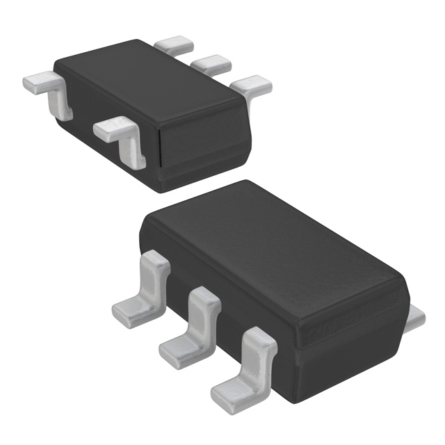
: SOT-25
Environmentally Friendly : EU RoHS Compliant, Pb Free
●For White LED drivers
●Smart phones / Mobile phones
●Mobile devices / terminals
●Digital still cameras
■TYPICAL PERFORMANCE
CHARACTERISTICS
■TYPICAL APPLICATION CIRCUIT
●XC9133B02A Series
LED:NSCW100 x 3
SBD:XBS053V15R,CL:TMK316J224KF
Efficiency : EFFI (%)
100
L:VLF3010S
90
80
NR3015
70
60
50
40
30
20
10
0
VIN=3.0V
0
5
10
15
20
25
30
LED Currrent : ILED (mA)
1/15
�XC9133 Series
■PIN CONFIGURATION
SOT-25 (TOP VIEW)
■PIN ASSIGNMENT
PIN NUMBER
SOT-25
PIN NAME
FUNCTIONS
1
2
3
4
5
Lx
VSS
FB
CE
VIN
Switch
Ground
Voltage Feedback
Chip Enable
Power Input
■CE PIN FUNCTION
CE PIN
OPERATIONAL STATE
H
L
Operation
Shut-down
■PRODUCT CLASSIFICATION
●Ordering Information
XC9133①②③④⑤⑥-⑦
DESIGNATOR
ITEM
SYMBOL
①
Lx Overvoltage Limit
B
Available
②③
FB Voltage
02
0.2V
④
Oscillation Frequency
A
1MHz
⑤⑥-⑦(*1)
Package (Order Unit)
(*1)
DESCRIPTION
MR
SOT-25 (3,000pcs/Reel)
MR-G
SOT-25 (3,000pcs/Reel)
The “-G” suffix denotes Halogen and Antimony free as well as being fully EU RoHS compliant.
2/15
�XC9133
Series
■BLOCK DIAGRAMS
●XC9133B02A
■ ABSOLUTE MAXIMUM RATINGS
Ta = 25℃
PARAMETER
SYMBOL
RATINGS
UNITS
VIN Pin Voltage
VIN
VSS – 0.3 ~ 7.0
V
Lx Pin Voltage
VLx
VSS – 0.3 ~ 22.0
V
FB Pin Voltage
VFB
VSS – 0.3 ~ 7.0
V
CE Pin Voltage
VCE
VSS – 0.3 ~ 7.0
V
Lx Pin Current
ILx
1000
mA
Power Dissipation
Pd
250
mW
Operating Ambient Temperature
Topr
- 40 ~ + 85
℃
Storage Temperature
Tstg
- 55 ~ +125
℃
3/15
�XC9133 Series
■ELECTRICAL CHARACTERISTICS
●XC9133B02AMR
Ta = 25℃
PARAMETER
FB Voltage
Output Voltage Range
Input Voltage Range
Supply Current 1
Supply Current 2
Stand-by Current
Oscillation Frequency(*1)
Maximum Duty Cycle
SYMBOL
VFB
VOUTSET
VIN
IDD1
IDD2
ISTB
fOSC
MAXDTY
Efficiency(*2)
EFFI
Current Limit
ILIM
Lx Overvoltage Limit
VLxOVL
Lx ON Resistance
Lx Leakage Current
RSWON
ILxL
CE High Voltage
VCEH
CE Low Voltage
VCEL
CE High Current
CE Low Current
FB High Current
FB Low Current
ICEH
ICEL
IFBH
IFBL
NOTE:
*Test circuit
*Test circuit
*Test circuit
*Test circuit
CONDITIONS
VIN=VLx, FB=0.4V
CE=0V, VLx=5.0V
When connected to ext.
components, VIN=3.6V, RLED=20Ω
When connected to ext. components,
VIN=3.6V
Voltage which Lx pin voltage
holding ”High” level
VIN ≧ 2.5V
VIN=3.6V, VLx=0.4V (*3)
Same as ISTB
CE applied voltage when Lx starts
oscillation
CE applied voltage which Lx pin
voltage holding “High” level
Same as IDD2
Same as ISTB
Same as IDD2
Same as ISTB
MIN.
0.19
VIN
2.5
0.8
86
TYP.
0.20
420
60
0
1.0
92
MAX.
0.21
17.5
6.0
720
140
1.0
1.2
98
UNIT.
V
V
V
μA
μA
μA
MHz
%
CIRCUIT
-
85
-
%
①
260
360
460
mA
④
18.0
19.0
22.0
V
②
-
2.4
0.0
1.0
Ω
μA
④
③
0.65
-
6.0
V
②
VSS
-
0.2
V
②
-0.1
-0.1
-0.1
-0.1
-
0.1
0.1
0.1
0.1
μA
μA
μA
μA
③
③
③
③
①: Unless otherwise stated, VIN=3.0V, VCE=3.0V, RLED=10Ω
②: Unless otherwise stated, VIN=3.0V, VCE=3.0V, VFB=0.0V, VPULL=5.0V, RPULL=100Ω
③: Unless otherwise stated, VIN=3.0V, VCE=3.0V, VFB=0.0V
④: Unless otherwise stated, VCE=3.0V, VPULL=5.0V
(*1):
The duty cycle is forcibly reduced when maximum duty cycle periods are repeated.
(*2):
LED NSPW310BS x 3, EFFI = {[(output voltage) x (output current)] / [(input voltage) x (input current)]} x 100
(*3):
VPULL is adjusted to make VLX 0.4V when the driver transistor is turned on.
4/15
①
①
①
②
③
③
②
②
�XC9133
Series
■TYPICAL APPLICATION CIRCUITS
●XC9133B02A
■EXTERNAL COMPONENTS
SYMBOL
L
VALUE
22μH
SBD (*1)
-
CIN
CL (*3)
4.7μF
0.22μF
PART NUMBER
VLF3010A-220MR
XBS053V15R (*2)
MA2Z720
JMK107BJ475MA-B
TMK107BJ224KA-B
MANUFACTURER
TDK
TOREX
PANASONIC
TAIYO YUDEN
TAIYO YUDEN
NOTE:
*1: Please use a Schottky barrier diode (SBD) with a low junction capacitance.
*2: For using the XBS053V15R with four white LEDs in series, please be noted with a direct reverse voltage (VR=20V) and a
repetitive peak reverse voltage (VRM=30V).
*3: Use ceramic capacitors processing a low temperature coefficient.
■OPERATIONAL EXPLANATION
The series consists of a reference voltage source, ramp wave circuit, error amplifier, PWM comparator, phase
compensation circuit, Lx overvoltage limit circuit, N-channel MOS driver transistor, current limiter circuit and others.
Phase compensation is performed on the resulting error amplifier output, to input a signal to the PWM comparator to
determine the turn-on time during switching. The PWM comparator compares, in terms of voltage level, the signal from
the error amplifier with the ramp wave from the ramp wave circuit, and delivers the resulting output to the N-channel MOS
driver transistor to cause the Lx pin to output a switching duty cycle. This process is continuously performed to ensure
stable output voltage. The current feedback circuit detects the N-channel MOS driver transistor's current for each
switching operation, and modulates the error amplifier output signal. This enables a stable feedback loop even when a
low ESR capacitor, such as a ceramic capacitor, is used, ensuring stable output voltage.
The reference voltage source provides the reference voltage to ensure stable output voltage of the IC.
The ramp wave circuit determines switching frequency. The 1MHz (TYP.) of frequency is fixed internally.
Clock pulses generated in this circuit are used to produce ramp waveforms needed for PWM operation.
The error amplifier is designed to monitor output voltage. The amplifier compares the reference voltage with the FB pin
voltage. When a feed-back voltage becomes lower than the reference voltage, an output voltage of the error amplifier is
increased. Gain and frequency characteristics of the error amplifier output are fixed internally as an optimize signal.
5/15
�XC9133 Series
■OPERATIONAL EXPLANATIONS (Continued)
The current limit circuit of the XC9133 series monitors the current flowing through the N-channel MOS driver transistor
connected to the Lx pin, and features a combination of the constant-current type current limit mode and the duty cycle limit
of the next pulse.
1When the driver current is greater than a specific levels, the constant-current type current limit function operates to
turn off the pulses from the Lx pin at any given timing.
2The IC controls the next pulse to be smaller than the first pulse.
Current Limit
The current will be off when the coil current
reached the value of the constant current limit.
Current Limit
Limit some duty pulses after the limit.
XC9133 series' Lx overvoltage limit circuit monitors the Lx pin voltage. When the Lx pin voltage exceeds than 19V (TYP.),
the IC performs the function of latching the OFF state of the driver transistor, and goes into operation suspension mode.
In suspension mode, operations can be resumed by restoring power to the VIN pin. The suspension mode does not mean
a complete shutdown, but a state in which pulse output is suspended; therefore, the internal circuitry remains in operation.
The XC9133 series' maximum duty cycle limit circuit monitors the duty cycle. When the maximum duty cycle is repeated
for a certain time, the IC controls the error amplifier output so that the duty cycle of the next pulse becomes smaller than
that of the first pulse.
The operation of the XC9133 series will enter into the shut down mode when a low level signal is input to the CE pin.
During the shut down mode, the supply current is 0μA (TYP.), with high impedance at the Lx pin. The IC starts its
operation with a high level signal to the CE pin. The input to the CE pin is a CMOS input and the sink current is 0μA
(TYP.). 100μs after disable, the IC goes into suspension mode and supply current is minimal. After this, the IC will be
in stand-by mode and the supply current will be 0μA (TYP.).
6/15
�XC9133
Series
■NOTES ON USE
Please connect the anode of a Schottky barrier diode and an inductor to the Lx pin.
The reference voltage is 200mV (TYP.). A resistor (RLED) should be connected to the FB pin for setting the cathode of
LEDs and a constant current value. The resistance value can be calculated by the following equation.
RLED=0.2 / ILED
ILED=Setting constant current value
Typical example:
ILED
5mA
10mA
RLED
40Ω
20Ω
ILED
13.3mA
20mA
RLED
15Ω
10Ω
An ENABLED state is reached when the CE voltage exceeds 0.65V and a DISABLED state when the CE Voltage falls below
0.2V.
Please connect an inductor and an input by-pass capacitor (CIN) to the VIN pin.
1. For temporary, transitional voltage drop or voltage rising phenomenon, the IC is liable to malfunction should the ratings be exceeded.
2. Torex places an importance on improving our products and their reliability.
We request that users incorporate fail-safe designs and post-aging protection treatment when using Torex products in their systems.
7/15
�XC9133 Series
■APPLICATION INFORMATION
1. Applying PWM signal to the CE pin
The XC9133 repeats on/off operations by a PWM signal applied to the CE pin. The magnitude of LED current, ILED,
when the diode is on, is determined by RLED. The magnitude is zero when the diode is off. The average of LED current
is proportional to the positive duty ratio of the PWM signal.
The frequency of the PWM signal can be controlled to the optimum value between 100Hz and 10kHz. With regard to the
amplitude of the PWM signal, the high level should be higher than the "H" voltage of CE, VCEH, and the low level, lower
than the "L" voltage of CE, VCEL.
10kHz, 3 series LED, ILED=20mA
10kHz, 4 series LED, ILED=20mA
20μs / div
20μs / div
1kHz, 3 series LED, ILED=20mA
1kHz, 4 series LED, ILED=20mA
200μs / div
200μs / div
2. Step-Wise Regulation of LED Current
In some applications, it may be necessary to incorporate step-wise regulation of LED current, ILED. Step-wise regulation
of LED illumination is achieved by connecting a switch element SW1 in parallel with RLED and in series with RLED1 and
turning SW1 on and off, as shown below. Choose a resistance of RLED so that the minimum necessary current is gained
when switch element SW1 is off. The resistance of RLED1 should be such that a desired increase of current passed
through the LED is gained when the switch element is on.
Ex.) Current ILED = 5mA and 15mA
RLED = 200mV / 5mA = 40 Ω
RLED1 = 200mV / (15mA – 5mA) = 20 Ω
Figure
8/15
Circuit using Step-wise Regulation of LED Current
�XC9133
Series
■APPLICATION INFORMATION (Continued)
3. Using DC Voltage
If in an application it is necessary to control the LED current by a variable DC voltage, illumination control of LED is
achieved by connecting R1 and R2 and applying a direct-current voltage to R2, as shown below.
When R1>>RLED, ILED which flows into LEDs can be calculated by the following equation;
ILED
ILED = (VREF - R1 / R2 (VDC - VREF)) / RLED
VREF = 0.2V (TYP.)
XC9133
FB
Ex.1) When R1 = 10k Ω, R2 = 100k Ω, RLED = 10 Ω,
In the range of 0.2V to 2.2V DC, ILED
(LED current) varies between 20mA to 0mA.
R2
VDC
R1
RLED
Figure
Circuit using DC voltage
Ex.2) When R1 = 10k Ω, R2 = 100k Ω, R3 = 10k Ω,
C1 = 0.1μF, RLED = 10Ω, the average LED current will
be 10mA by inputting a PWM signal of CE ‘H’ level:
2.2V, CE ’L’ level: 0V, duty cycle: 50%, oscillation
frequency: 100Hz. As well as the way of dimming
control by applying the PWM signal to the CE pin, the
average LED current increases proportionally with the
positive duty cycle of the PWM signal.
Figure
Circuit inputting a PWM signal to the FB pin
When the input voltage (VIN) is high, minimum illumination may occur even if the CE pin is in the disable state. If this
happens, please connect a transistor to between the LED and the FB pin. By driving the CE signal in-phase and cutting
the pass to current, the minimum illumination can be prevented.
SBD
XBS053V15R
L:22μH
VLF3010A
VIN
3.6V
(3.2V~6.0V)
CIN
4.7μF
VIN
Lx
XP151A12A2
CE
FB
VSS
Figure
CL
0.22μF
(base)
RLED
10Ω
20mA
Circuit Prevent Emission Caused by White LEDs Leakage
9/15
�XC9133 Series
■APPLICATION INFORMATION (Continued)
It is possible to illuminate three-series two parallel white LEDs, six in total, using an input voltage VIN≧3.2V.
Figure
Circuit Illumination of Six in Total White LEDs
An LED current 65mA (MAX.) can be supplied to two white LEDs.
Figure
10/15
Circuit using a Flash
�XC9133
Series
■APPLICATION INFORMATION (Continued)
Supply source of the step-up circuit can be used separately from VIN pin.
Circuit example of separating supply source of
the step-up circuit from VIN pin ( 3 LEDs)
Circuit example of separating supply source of
the step-up circuit from VIN pin ( 2 LEDs)
Note: Please input 2.5V~6V to the VIN pin when you use.
If white LEDs are opened or damaged, the FB pin is pulled down, so that the operating duty ratio reaches the maximum.
Accordingly, the output voltage continues to increase, possibly causing the Lx pin voltage to exceed the absolute maximum
rating of 22V.
If white LEDs are opened or damaged, the detector built in the Lx pin causes the IC to stop oscillating, preventing excessive
increase of the output voltage. However, the detector may detect an overvoltage if the Lx pin voltage exceeds 18V, which is
the overvoltage limit, even when no LEDs are open. Therefore, care must be taken if four LEDs each having a forward
voltage of 4.45V or more are connected in series.
The XC9133 series has no soft-start circuit built-in in order to minimize delay at startup. The inrush current can reach up
to the current limit ILIM.
In some cases, overshoot can occur.
11/15
�XC9133 Series
■APPLICATION INFORMATION (Continued)
1. In order to stabilize VIN's voltage level, we recommend that an input by-pass capacitor (CIN) be connected as close as
possible to the VIN & VSS pins.
2. Please mount each external component as close to the IC as possible.
3. Wire external components as close to the IC as possible and use thick, short connecting traces to reduce the circuit
impedance.
4. Make sure that the PCB GND traces are as thick as possible, as variations in ground potential caused by high ground
currents at the time of switching may result in instability of the IC.
●XC9133B Series Pattern Layout
12/15
�XC9133
Series
■TEST CIRCUITS
●Circuit ① (XC9133B02A Series)
L:22uH
SBD
CDRH3D16 XBS053V15R
CIN
VIN
VIN
Lx
CE
FB
4.7μF
(ceramic)
CL
VSS
VCE
0.22μF
(ceramic)
RLED
●Circuit ②
V
●Circuit ③
●Circuit ④
1. The measurement method of LX ON Resistance RSWON
Using the circuit ④, Lx ON resistance can be measured by adjusting VPULL voltage to set Lx voltage VLX 0.4V when the
driver transistor is ON.
The oscilloscope is used for measuring the Lx voltage when the driver transistor is ON.
RSWON = 0.4 / ((VPULL - 0.4) /10)
2. The measurement method of current limit ILIM
Using the circuit ④, current limit ILIM can be calculated by the equation including VPULL voltage when FB voltage is
decreased while VPULL voltage is adjusted and Lx voltage VLX when the driver transistor is ON.
The oscilloscope is used for measuring the Lx voltage when the driver transistor is ON.
ILIM = (VPULL - VLX) / RPULL
RPULL=10Ω
13/15
�XC9133 Series
■PACKAGING INFORMATION
●SOT-25
(unit : mm)
2.9±0.2
+0.1
0.4 -0.05
5
4
0~0.1
1
2
3
+0.1
0.15 -0.05
(0.95)
1.9±0.2
■ MARKING RULE
SOT25
●SOT-25
5
①
1
4
②
③
2
④
⑤
3
① represents product series
MARK
PRODUCT SERIES
N
XC9133****M*
② represents Lx overvoltage limit
MARK
Lx OVERVOLTAGE LIMIT
PRODUCT SERIES
B
Available
XC9133****M*
MARK
OSCILLATION FREQUENCY
PRODUCT SERIES
A
1MHz
XC9133****M*
③ represents oscillation frequency
④⑤ represents production lot number
01 to 09, 0A to 0Z, 11 to 9Z, A1 to A9, AA to Z9, ZA to ZZ repeated.
(G, I, J, O, Q, W excepted)
* No character inversion used.
14/15
�XC9133
Series
1.
The product and product specifications contained herein are subject to change without notice to
improve performance characteristics. Consult us, or our representatives before use, to confirm that
the information in this datasheet is up to date.
2.
The information in this datasheet is intended to illustrate the operation and characteristics of our
products. We neither make warranties or representations with respect to the accuracy or
completeness of the information contained in this datasheet nor grant any license to any intellectual
property rights of ours or any third party concerning with the information in this datasheet.
3.
Applicable export control laws and regulations should be complied and the procedures required by
such laws and regulations should also be followed, when the product or any information contained in
this datasheet is exported.
4.
The product is neither intended nor warranted for use in equipment of systems which require
extremely high levels of quality and/or reliability and/or a malfunction or failure which may cause loss
of human life, bodily injury, serious property damage including but not limited to devices or equipment
used in 1) nuclear facilities, 2) aerospace industry, 3) medical facilities, 4) automobile industry and
other transportation industry and 5) safety devices and safety equipment to control combustions and
explosions. Do not use the product for the above use unless agreed by us in writing in advance.
5.
Although we make continuous efforts to improve the quality and reliability of our products;
nevertheless Semiconductors are likely to fail with a certain probability. So in order to prevent
personal injury and/or property damage resulting from such failure, customers are required to
incorporate adequate safety measures in their designs, such as system fail safes, redundancy and
fire prevention features.
6.
Our products are not designed to be Radiation-resistant.
7.
Please use the product listed in this datasheet within the specified ranges.
8.
We assume no responsibility for damage or loss due to abnormal use.
9.
All rights reserved. No part of this datasheet may be copied or reproduced unless agreed by Torex
Semiconductor Ltd in writing in advance.
TOREX SEMICONDUCTOR LTD.
15/15
�