XC9301/XC9302 Series
ETR0601_001c
PWM,PWM/PFM Switching Step-Up & Down DC/DC Converter Controller ICs
☆Green Operation Compatible
■GENERAL DESCRIPTION
The XC9301/XC9302 series are step-up/down DC/DC converter controller ICs with fast, low ON resistance drivers built-in. A
versatile, large output current, step-up/down DC/DC converter can be realized using only 4 type of basic external components
two transistors, one inductor, two diodes and capacitors.
Output voltage is selectable in 0.1V increments within a 2.4V ~ 6.0V (±2.5% accuracy) range and switching frequency is set
at 180kHz or 300kHz.
The XC9302 series switches from PWM to PFM control during light loads and the series offers high efficiencies from light
loads through to large output currents.
Soft-start time is internally set to 10ms which offers protection against inrush currents when the power is turned on and also
against voltage overshoot.
During shutdown (CE pin = L), consumption current can be reduced to as little as 0.5μA or less.
■APPLICATIONS
■FEATURES
●Mobile phones
Input Voltage Range
●PDAs
Output Voltage Range : 2.4V ~ 6.0V (±2.5% accuracy)
●Palmtop computers
(selectable in 0.1V increments)
Oscillation Frequency : 180kHz, 300kHz
●Portable audio equipment
●Various power supplies
: 2.0V ~ 10V
(±15% accuracy)
Output Current
: 250mA(VIN=2.4V, VOUT=3.3V)
Efficiency
: 81%(TYP.) @ VOUT=5.0V,
Stand-By
: ISTB = 0.5μA (MAX.)
78%(TYP.) @ VOUT=3.3V
Maximum Duty Cycle : 85%(TYP.)
Package
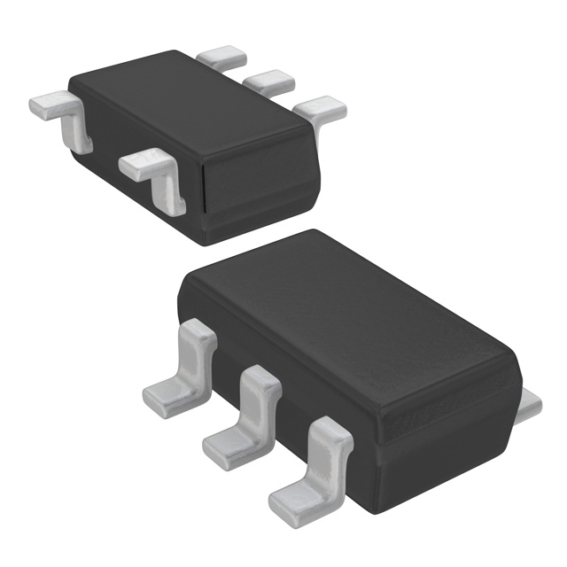
: SOT-25
Environmentally Friendly: EU RoHS Compliant, Pb Free
■TYPICAL PERFORMANCE
CHARACTERISTICS
XC9302A502 (180kHz, VOUT5.0V)
●Efficiency vs. Output Current
PSW=XP162A12A6PR,CL=47μF ((MCE series, Tantalum))×2,
NSW=XP161A1265PR,CIN=220μF (Electrolytic, PJ type),SD=U2FWJ44N,RDD=10Ω,
L=22μH (CR54),CDD=47μF (MCE series, Tantalum)
100
Efficiency:EFFI(%)
■TYPICAL APPLICATION CIRCUIT
80
60
VIN=2V
40
4V
20
6V
0
0. 1
1
10
100
1000
Output Current:IOUT(mA)
1/13
�XC9301/XC9302 Series
■PIN CONFIGURATION
■PIN ASSIGNMENT
PIN NUMBER PIN NAME
FUNCTION
1
GND
Ground
2
VDD
Power Supply
3
EXT/
External Tr. Drive
4
VOUT
Output Voltage Monitor
5
CE
Chip Enable
■PRODUCT CLASSIFICATION
●Ordering Information
XC9301①②③④⑤⑥-⑦
(*1)
XC9302①②③④⑤⑥-⑦
(*1)
: PWM control
: PWM/PFM switching control
DESIGNATOR
DESCRIPTION
SYMBOL
①
Standard
A
②③
Output Voltage
20~60
④
Oscillation Frequency
⑤⑥-⑦
(*1)
(*2)
Packages
Taping Type (*2)
DESCRIPTION
Fixed
e.g. VOUT=3.0V→②=3, ③=0, VOUT=5.3V→②=5, ③=3
2
180kHz
3
300kHz
MR-G
SOT-25
The “-G” suffix indicates that the products are Halogen and Antimony free as well as being fully RoHS compliant.
The device orientation is fixed in its embossed tape pocket. For reverse orientation, please contact your local Torex sales office or
representative. (Standard orientation: ⑤R-⑦, Reverse orientation: ⑤L-⑦)
■BLOCK DIAGRAM
2/13
�XC9301/XC9302
Series
■ABSOLUTE MAXIMUM RATINGS
Ta = 25℃
PARAMETER
SYMBOL
RATINGS
UNITS
VDD Pin Voltage
VDD
-0.3∼12.0
V
VOUT Pin Voltage
VOUT
-0.3∼12.0
V
CE Pin Voltage
VCE
-0.3∼12.0
V
EXT/ Pin Voltage
VEXT/
-0.3∼VDD+0.3
V
EXT/ Pin Current
IEXT/
±100
mA
Power Dissipation
Pd
150
mW
Operating Temperature Range
Topr
-40∼+85
℃
Storage Temperature Range
Tstg
-40∼+125
℃
3/13
�XC9301/XC9302 Series
■ELECTRICAL CHARACTERISTICS
XC9301x332MR, XC9302x332MR
PARAMETER
SYMBOL
Output Voltage
VOUT
Supply Voltage
VDD
Supply Current 1
IDD1
Supply Current 2
IDD2
Stand-By Current
ISTB
Oscillation Frequency
FOSC
Maximum Duty Ratio
MAXDTY
PFM Duty Ratio
Efficiency
(*1)
(*2)
PFMDTY
EFFI
Soft-Start Time
CE 'H' Voltage
CE 'L' Voltage
EXT/ 'H' ON Resistance
EXT/ 'L' ON Resistance
TSS
VCEH
VCEL
REXTBH
REXTBL
(VOUT=3.3V, FOSC=180kHz)
MIN.
TYP.
3.218
3.300
2.0
VOUT=CE: Setting output voltage × 0.95 applied
80
VOUT=CE: Setting output voltage + 0.5 applied
15
VOUT: Setting output voltage × 0.95 applied,
CE=0V
VDD=VOUT=CE:
153
180
Setting output voltage × 0.95 applied
VDD=VOUT=CE:
78
85
Setting output voltage × 0.95 applied
No Load
15
25
VDD=VIN=CE:
78
Setting output voltage × 0.95 applied
5.0
10.0
VOUT: Setting output voltage × 0.95 applied
0.65
VOUT: Setting output voltage × 0.95 applied
Same as IDD1, VEXT/ = VOUT - 0.4V
29
Same as IDD1, VEXT/ = 0.4V
19
CONDITIONS
MAX.
3.383
10.0
140
26
Ta=25℃
UNITS
V
V
μA
μA
0.5
μA
207
kHz
92
%
35
%
-
%
20.0
0.20
43
27
ms
V
V
Ω
Ω
Test Conditions: Unless otherwise stated, VDD = 3.3V, IOUT = 130mA
NOTE: *1: XC9302 series only
*2: EFFI={[(output voltage) × (output current)] / [(input voltage) × (input current)]} × 100
XC9301x333MR, XC9302x333MR
PARAMETER
SYMBOL
Output Voltage
VOUT
Supply Voltage
VDD
Supply Current 1
IDD1
Supply Current 2
IDD2
Stand-By Current
ISTB
Oscillation Frequency
FOSC
Max. Duty Ratio
MAXDTY
PFM Duty Ratio
Efficiency (*2)
(*1)
Soft-Start Time
CE 'H' Voltage
CE 'L' Voltage
EXT/ 'H' ON Resistance
EXT/ 'L' ON Resistance
PFMDTY
EFFI
TSS
VCEH
VCEL
REXTBH
REXTBL
(VOUT=3.3V, FOSC=300kHz)
CONDITIONS
MIN.
3.218
2.0
VOUT=CE: Setting output voltage × 0.95 applied
VOUT=CE: Setting output voltage + 0.5 applied
VOUT: Setting output voltage × 0.95 applied,
CE=0V
VDD=VOUT=CE:
255
Setting output voltage × 0.95 applied
VDD=VOUT=CE:
78
Setting output voltage × 0.95 applied
No Load
15
VDD=VIN=CE:
Setting output voltage × 0.95 applied
5.0
VOUT: Setting output voltage × 0.95 applied
0.65
VOUT: Setting output voltage × 0.95 applied
Same as IDD1, VEXT/ = VOUT - 0.4V
Same as IDD1, VEXT/ = 0.4V
-
Ta=25℃
UNITS
V
V
μA
μA
TYP.
3.300
130
20
MAX.
3.383
10.0
200
35
-
0.5
μA
300
345
kHz
85
92
%
25
78
35
-
%
%
10.0
29
19
20.0
0.20
43
27
ms
V
V
Ω
Ω
Test Conditions: Unless otherwise stated, VDD = 3.3V, IOUT = 130mA
NOTE: *1: XC9302 series only
*2: EFFI={[(output voltage) × (output current)] / [(input voltage) × (input current)]} × 100
■TYPICAL APPLICATION CIRCUIT
External Components
PSW: XP162A12 (SOT-89, TOREX)
NSW: XP161A12 (SOT-89, TOREX)
L
: 22μH (CR54, SUMIDA)
SD : U2FWJ44N ( Schottky, TOSHIBA )
CL : 16V, 47μF×2 (Tantalum, MCE series, NICHICON )
CIN : 16V, 22μF (Tantalum, MCE series, NICHICON )
220μF (Electrolytic, NICHICON, PJ type)
4/13
�XC9301/XC9302
Series
■OPERATIONAL EXPLANATION
The XC9301/9302 series are PWM (PWM/PFM switching) step-up/down DC/DC converter controller ICs. The XC9302 series
switches to PFM operations during light loads and is very efficient over a wide range in relation to load. Further, the efficiency
can be maintained over a wide input voltage range as both step-up & step-down operations are PWM controlled. Output
voltage settings are laser trimmed.
P-ch MOSFET (PSW) = ON, N-ch MOSFET (NSW) = ON: Current flows from VIN via PSW, L, NSW, to GND: L is charged.
P-ch MOSFET (PSW) = OFF, N-ch MOSFET (NSW) = OFF: Current flows from GND via SD1, L, SD2, to VOUT: VOUT rises
due to the charge stored at L.
By comparing VOUT with the internal reference voltage, the ON TIME vs. OFF TIME ratio can be regulated & output stability
can be protected.
The error amplifier is used as an output voltage monitor. It compares the reference voltage with the feedback from the voltage
divided by the internal resistor. Should a voltage higher than the reference voltage be fedback, the output of the error amp will
increase.
The PWM comparator compares the output of the error amp with the ramp wave. When the voltage at the output of the error
amp is low, the EXT/ pin will be low level (Switching ON time).
The ramp wave generator generates the switching frequency's ramp wave.
With the XC9302 series, control is automatically switched between PWM and PFM according to the size of the load.
The start up of the Vref voltage at the error amp's input is gradual due to the internal capacitor and low current circuit.
Because of this soft-start function, the operations of the error amp's 2 inputs are balanced and the EXT/ pin's ON TIME can
be manipulated to produce longer ON times. Further, with the U.V.L.O. function, the signal will be such so as not to turn the
MOSFET switch ON until any instability in the internal circuit stabilizes during soft-start time. Even in cases where input
voltage is so low as to produce instability in the IC, the U.V.L.O. function will operate and the MOSFET switch will be turned
OFF.
5/13
�XC9301/XC9302 Series
■OPERATIONAL EXPLANATION (Continued)
●Product Selection (Notes)
XC9301/02 series is a group of PFM controlled (XC9302 series switches from PWM to PFM control during light loads)
step-up and down DC/DC converters. The series is highly efficient with a wide range of input voltage since its stepping-up
and down operation is controlled by PWM movements. In general, there are several methods available for obtaining a
stable output voltage at such times when input voltage is changing from being higher than the established output voltage to
being lower than the established output voltage. Each method has its merits and demerits but is essential that a method,
which provides the best results in terms of input and output under actual operating conditions. Below, two methods are
highlighted and their respective performances in terms of efficiency are compared. This is an efficiency comparison of two
ways, step-up DC/DC converter + VR and step-up & down DC/DC converter.
[Step-Up DC/DC Converter + VR] (XC6361/62)
◆Step-up mode (Input voltage < setting output voltage + 0.4V)
After input voltage has been stepped-up to setting output voltage + 0.4V by the step-up DC/DC converter, the output
voltage will be regulated to the set value by the VR. (0.4V loss via the VR)
◆Step-down mode (Input voltage > setting output voltage + 0.4V)
After input voltage has been stepped-up to setting output voltage + 0.4V by the step-up DC/DC converter, the output
voltage will be regulated to the set value by the VR. (Dropout voltage loss via the VR)
[Step-Up & Down DC/DC Converter] (XC9301/02)
◆Setting output voltage obtained as a result of the automatic switching operations of the IC regardless of the difference
between input voltage and set output voltage.
Efficiency[%]
Input Voltage vs. Efficiency
XC6361(STEP-UP DCDC+VR)
90
85
80
75
70
65
60
55
50
45
40
IOUT=10mA 100mA 200mA
XC9301(STEP-UP/DOWN DCDC
IOUT=10mA 100mA 200mA
Set Output Voltage+0.4V
Step-Up Mode
2
3
Step-Down Mode
4
5
6
7
8
Input Voltage [V]
The above graph shows that over a wide input voltage range, the efficiency of the XC9301/02 is more or less constant. On the
other hand, the efficiency of the XC6361/62 is clearly shown to decrease as input voltage increases. In step-down mode in
particular, the efficiency of the XC9301/02 is much better than the XC6361/62. In applications that use either a standard dry 3
cell battery or a 2 cell lithium Ion battery to obtain an output of 3.3V, for example, the efficiency of the XC9301/02 series is
again much better. Because the XC9301/02 series does not have a series regulator output, we recommend a test with
samples for use in applications where ripple voltage is a problem.
●External Components Selection (Notes)
The performance of the DC/DC converter IC circuit is heavily reliant upon the performance of the surrounding circuitry and
components. In particular, since the VF voltage of the Schottky Diode used will have a direct effect upon efficiency, the
smaller the diode, the better the efficiency obtainable. (Refer to the graph below)
●It is also recommended that a switching MOSFET with a small ON resistance be used. With the XC9301/02, an ON
resistance of 500mΩ or less is recommended.
●
VOUT=3.3V, IOUT=100mA
Efficiency[%]
85
80
VIN=2.4V
VIN=3.0V
75
VIN=4.5V
70
65
0.2
0.4
VF Voltage[V]
6/13
�XC9301/XC9302
Series
■OPERATIONAL EXPLANATION (Continued)
●Demo Board Version 1.1
External Components
Demo Board Connection Layout
PSW : XP162A12 (SOT-89)
NSW : XP161A12 (SOT-89)
→suitable for SOT-23, SOT-89, CPH-6
L
: 22μH (CR54, SUMIDA)
→suitable for CR43∼CR105
SD : U2FWJ44N (Schottky, TOSHIBA)
→suitable for MA720, MA735, U2FWJ44N
CL : 16V, 47μF×2 (Tantalum, MCE series, NICHICON)
→suitable for 1005 type∼D2 Package
CIN : 16V, 22μF (Tantalum, MCE series, NICHICON)
16V, 220μF (Electrolytic, NICHICON, PJ type)
JP3: Must be connected
JP2: To be connected if using SW (CE pin fixed to VIN)
* Use tinned copper wire for the VIN pin, VOUT pin, GND pin, JP2, and JP3.
* Connect test pins for the TP1, TP2, TP3, and CE.
Note:
Oscillation may occur as a result of input voltage
instability when the output current is large. At such
times, we recommend that in place of the 220μF, PJ
type capacitor, you connect R1 & C1 as shown in the
diagram on the right hand side. (In case of demo
boards version 1.1, cut the pattern wire of R1
connecting point, then connect R1.)
7/13
�XC9301/XC9302 Series
■TYPICAL PERFORMANCE CHARACTERISTICS
XC9302A332 (PWM/PFM switching control, 180kHz, VOUT=3.3V)
(1) Output Voltage vs. Output Current (Topr=25℃)
(2) Efficiency vs. Output Current (Topr=25℃)
(3) Ripple Voltage vs. Output Current (Topr=25℃)
Output Current=lout (mA)
External Components
PSW : XP162A12A6PR
NSW : XP161A1265PR
SD
: U2FWJ44N
L
: 22μH (CR54)
8/13
CL : 47μF (MCE series, Tantalum) × 2
CIN : 220μF (Electrolytic, PJ type)
RDD : 10Ω
CDD : 47μF (MCE series, Tantalum)
VCE=VIN
�XC9301/XC9302
Series
■TYPICAL PERFORMANCE CHARACTERISTICS (Continued)
XC9302A332 (PWM/PFM switching control, 180kHz, VOUT=3.3V) (Continued)
(4) Load Transient Response (Topr=25℃)
VIN=3.0V
VIN=3.0V
External Components
PSW : XP162A12A6PR
NSW : XP161A1265PR
SD
: U2FWJ44N
L
: 22μH (CR54)
CL : 47μF (MCE series, Tantalum) × 2
CIN : 220μF (Electrolytic, PJ type)
RDD : 10Ω
CDD : 47μF (MCE series, Tantalum)
VCE=VIN
9/13
�XC9301/XC9302 Series
■TYPICAL PERFORMANCE CHARACTERISTICS (Continued)
XC9302A502 (PWM/PFM switching control, 180kHz, VOUT=5.0V)
(1) Output Voltage vs. Output Current (Topr=25℃)
(2) Efficiency vs. Output Current (Topr=25℃)
(3) Ripple Voltage vs. Output Current (Topr=25℃)
External Components
PSW : XP162A12A6PR
NSW : XP161A1265PR
SD
: U2FWJ44N
L
: 22μH (CR54)
10/13
CL : 47μF (MCE series, Tantalum) × 2
CIN : 220μF (Electrolytic, PJ type)
RDD : 10Ω
CDD : 47μF (MCE series, Tantalum)
VCE=VIN
�XC9301/XC9302
Series
■TYPICAL PERFORMANCE CHARACTERISTICS (Continued)
XC9302A502 (PWM/PFM switching control, 180kHz, VOUT=5.0V) (Continued)
(4) Load Transient Response (Topr=25℃)
VIN=4.0V
VIN=4.0V
External Components
PSW : XP162A12A6PR
NSW : XP161A1265PR
SD
: U2FWJ44N
L
: 22μH (CR54)
CL : 47μF (MCE series Tantalum) ×2
CIN : 220μF (Electrolytic, PJ type)
RDD : 10Ω
CDD : 47μF (MCE series Tantalum)
VCE=VIN
11/13
�XC9301/XC9302 Series
■PACKAGING INFORMATION
●SOT-25
■MARKING RULE
①represents the product series
●SOT-25
5
①
1
4
②
③ ④
2
3
MARK
PRODUCT SERIES
A
K
XC9301AxxxMx
XC9302AxxxMx
②represents the integer of the output voltage and oscillation frequency
OUTPUT
VOLTAGE (V)
2.x
3.x
4.x
5.x
6.x
MARK
FREQUENCY=180kHz
FREQUENCY=300kHz
(XC9301/XC9302Axx3Mx)
(XC9301/XC9302Axx2Mx)
2
3
4
5
6
2
3
4
5
6
③represents decimal number of output voltage and oscillation frequency
OUTPUT
VOLTAGE (V)
0.x
1.x
2.x
3.x
4.x
5.x
6.x
7.x
8.x
9.x
MARK
FREQUENCY=180kHz
FREQUENCY=300kHz
(XC9301/XC9302Axx2Mx)
(XC9301/XC9302Axx3Mx)
0
1
2
3
4
5
6
7
8
9
④represents production lot number
0 to 9, A to Z reverse character 0 to 9, A to Z repeated
(G, I, J, O, Q, W excluded)
12/13
A
B
C
D
E
F
H
K
L
M
�XC9301/XC9302
Series
1. The products and product specifications contained herein are subject to change without
notice to improve performance characteristics.
Consult us, or our representatives
before use, to confirm that the information in this datasheet is up to date.
2. We assume no responsibility for any infringement of patents, patent rights, or other
rights arising from the use of any information and circuitry in this datasheet.
3. Please ensure suitable shipping controls (including fail-safe designs and aging
protection) are in force for equipment employing products listed in this datasheet.
4. The products in this datasheet are not developed, designed, or approved for use with
such equipment whose failure of malfunction can be reasonably expected to directly
endanger the life of, or cause significant injury to, the user.
(e.g. Atomic energy; aerospace; transport; combustion and associated safety
equipment thereof.)
5. Please use the products listed in this datasheet within the specified ranges.
Should you wish to use the products under conditions exceeding the specifications,
please consult us or our representatives.
6. We assume no responsibility for damage or loss due to abnormal use.
7. All rights reserved. No part of this datasheet may be copied or reproduced without the
prior permission of TOREX SEMICONDUCTOR LTD.
13/13
�