XCL102/XCL103 Series
ETR28011-005
Inductor Built-in Step-up “micro DC/DC” Converter (micro DC/DC)
☆Green Operation Compatible
■GENERAL DESCRIPTION
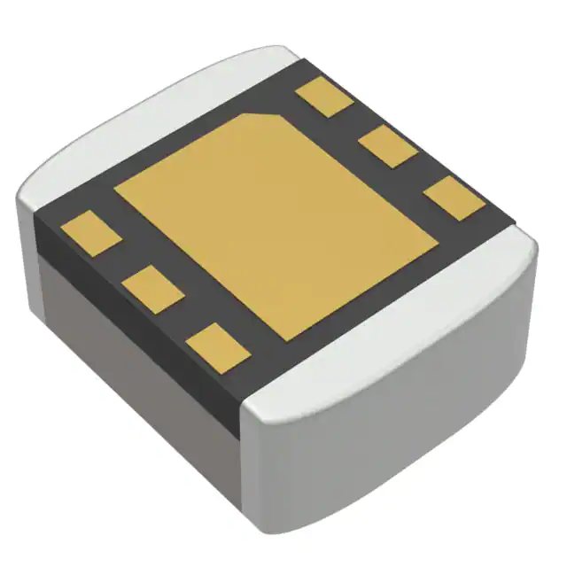
The XCL102/XCL103 series is a synchronous step-up micro DC/DC converter which integrates an inductor and a control IC in
one tiny package (2.0mm×2.5mm, h=1.0mm). A stable step-up power supply is configured using only two capacitors connected
externally. An internal coil simplifies the circuit and enables minimization of noise and other operational trouble due to the circuit
wiring. A wide operating voltage range of 0.65V to 6.0V enables support for applications that require an internally fixed output
voltage (2.2V to 5.5V). PWM control (XCL102) or automatic PWM/PFM switching control (XCL103) can be selected.
During the devices enter stand-by mode, XCL102D/XCL103D types prevent the application malfunction by CL Discharge
Function which can quickly discharge the electric charge at the output capacitor (CL). XCL102/XCL103E types is able to drive
Real Time Clock etc.
■APPLICATIONS
● Portable equipment
● Beauty & health equipment
● Wearable devices
● Game & Hobby
● PC Peripherals
● Devices with 1~3 Alkaline,
1~3 Nickel Hydride, 1 Lithium and 1 Li-ion
■FEATURES
Input Voltage Range
Fixed Output Voltage
Oscillation Frequency
Input Current
Output Current
Control Mode Selection
Load Transient Response
Protection Circuits
Functions
Output Capacitor
Operating Ambient Temperature
Package
Environmentally Friendly
■TYPICAL APPLICATION CIRCUIT
7
L1
VBAT
1 VBAT
VOUT 6
2 GND
Lx 5
CIN
VCE
: operating hold voltage 0.65V ~ 6.0V
: Start-up voltage
0.9V ~ 6.0V
: 2.2V ~ 5.5V (0.1V increments)
: 3.0MHz
: 0.8A
: 450mA @VOUT=5.0V, VBAT=3.3V
280mA @VOUT=3.3V, VBAT=1.8V
: PWM (XCL102)
PWM/PFM (XCL103)
:100mV@VOUT=3.3V, VBAT=1.8V
,IOUT=1mA→200mA
: Over-current limit (Integral latch method)
Output short-circuit protection
: Soft-start
Load Disconnection (D type)
CL Auto Discharge (D type)
Bypass Switch (E type)
: Ceramic Capacitor
: -40℃ ~ 85℃
: CL-2025-02
: EU RoHS Compliant, Pb Free
:
:
TYPICAL PERFORMANCE
:
:
CHARACTERISTICS
:XCL103D503CR-G/XCL103E503CR-G
:
:
:
:
:
■
VOUT
CL
3 CE
GND 4
L2
8
1/24
�XCL102/XCL103 Series
■ BLOCK DIAGRAM
● D Type
L2
L1
Inductor
LX
Load Disconnect
Controller
Phase
Compensation
CFB
RFB1
Error Amp.
FB
Current sense
Short-circuit
protection
Latch Timer
VOUT
PWM
Comparator
Buffer
Drive
CL
Discharge
RFB2
GND
PFM/PWM
Controller Logic
Vref with
Soft Start
CE
VOUT
RAMP Wave
Generator
OSC
VOUT
CE Controller
Logic
VDD
VBAT
VDD MAX
* Diodes inside the circuits are ESD protection diodes and parasitic diodes.
* XCL102 series chooses only PWM control.
●E Type
L2
L1
Inductor
LX
Load Disconnect
Controller
Phase
Compensation
CFB
RFB1
Error Amp.
FB
Current sense
Short-circuit
protection
Latch Timer
VOUT
VOUT
PWM
Comparator
Buffer
Drive
RFB2
GND
PFM/PWM
Controller Logic
Vref with
Soft Start
CE
CE Controller
Logic
RAMP Wave
Generator
OSC
VOUT
VDD
Bypass SW
VDD MAX
* Diodes inside the circuits are ESD protection diodes and parasitic diodes.
* XCL102 series chooses only PWM control.
2/24
VBAT
�XCL102/XCL103
Series
■PRODUCT CLASSIFICATION
●Ordering
Information
XCL102①②③④⑤⑥-⑦ PWM control
XCL103①②③④⑤⑥-⑦ PWM/PFM automatic
DESIGNATOR
ITEM
SYMBOL
①
Type
D
E
②③
Output Voltage
22 ~ 55
Oscillation Frequency
3
Package (Order Unit)
CR-G
④
⑤⑥-⑦
(*1)
(*1)
DESCRIPTION
Refer to Selection Guide
Output Voltage options
e.g.)3.3V → ②=3, ③=3
5.0V → ②=5, ③=0
3.0MHz
CL-2025-02 (3,000pcs/Reel)
The ”-G” suffix indicates that the products are Halogen and Antimony free as well as being fully EU RoHS compliant.
●Selection guides
Output
Chip
Voltage
Enable
D
Fixed
Yes
Fixed
E
Fixed
Yes
Fixed
Type
(*1)
Soft-Start
Current Limit
Short Protection
CL Auto-
Shutdown
With Latch
Discharge
at CE=”L"
Yes
Yes
Yes
-
Yes
(with integral latch)
Yes
(with integral latch)
Complete Output
Disconnect (*1)
Input-to-Output
Bypass (*1)
The VOUT pin cannot be connected to the output pin of another power supply such as AC adapter, etc.
■PIN CONFIGURATION
7 L1
VOUT 6
1 VBA T
Lx 5
2 GN D
3 CE
GN D 4
8 L2
(BOTTOM VIEW)
* The dissipation pad should be solder-plated in recommended mount pattern and metal masking
to enhance mounting strength and heat release. If the pad needs to be connected to other pins,
it should be connected to the GND (No. 2,4) pin.
■PIN ASSIGNMENT
PIN NUMBER
PIN NAME
FUNCTIONS
1
2
3
4
5
6
7
8
VBAT
GND
CE
GND
Lx
VOUT
L1
L2
Power Input
Ground
Chip Enable
Ground
Switching
Output Voltage
Inductor Electrodes
3/24
�XCL102/XCL103 Series
■FUNCTION CHART
PIN NAME
CE
SIGNAL
STATUS
L
Stand-by
H
Active
* Do not leave the CE pin open.
■ABSOLUTE MAXIMUM RATINGS
PARAMETER
SYMBOL
RATINGS
UNITS
VBAT Pin Voltage
VBAT
-0.3 ~ 7.0
V
Lx Pin Voltage
VLx
-0.3 ~ 7.0
V
VOUT Pin Voltage
VOUT
-0.3 ~ 7.0
V
CE Pin Voltage
VCE
-0.3 ~ 7.0
1000 (40mm x 40mm Standard
Power Dissipation (Ta=25℃)
Pd
Operating Ambient Temperature
Topr
-40 ~ 85
℃
Storage Temperature
Tstg
-55 ~ 125
℃
* GND are standard voltage for all of the voltage.
(*1)
V
The power dissipation figure shown is PCB mounted and is for reference only.
The mounting condition is please refer to PACKAGING INFORMATION.
4/24
board) (*1)
mW
�XCL102/XCL103
Series
■ELECTRICAL CHARACTERISTICS
Ta=25℃
PARAMETER
SYMBOL
BAT Voltage
VBAT
Output Voltage
VOUT
Operation Start Voltage
VST1
Operation Hold Voltage
MIN.
TYP.
MAX.
UNITS
CIRCUIT
-
-
6.0
V
①
V
⑤
RL=1kΩ
-
-
0.90
V
①
VHLD
RL=1kΩ
-
0.65
-
V
①
Iq
VOUT=VBAT= VOUT(T)+0.5V
-
26
40
μA
③
IDD
VOUT=VBAT= VOUT(T)-0.2V
-
3.0
mA
③
Oscillation Frequency
fOSC
VBAT= VOUT(T)×0.5, IOUT=100mA
2.4
3.0
3.6
MHz
①
Maximum Duty Cycle
DMAX
VBAT=1.2V, VOUT= VOUT(T)-0.2V
88
93
98
%
⑤
Minimum Duty Cycle
DMIN
VOUT=VBAT= VOUT(T)+0.5V
-
-
0
%
⑤
-
165
230
mA
①
-
86(*3)
-
%
①
VBAT= VOUT(T)×0.6, IOUT= 100mA
-
90(*3)
-
%
①
-
0
1.0
μA
⑦
-
0.3(*2)
-
Ω
④
-
0.3(*3)
-
Ω
①
-
0
1.0
μA
⑦
A
⑥
25
100
365
μs
⑥
0.9
1.2
1.5
V
①
-
(*3)
-
V
①
0.2
0.5
1.0
ms
⑤
Quiescent Current
(XCL103 only)
Supply Current
PFM Switching Current
(XCL103 only)
Efficiency
(XCL103 only)
IPFM
EFFI
CONDITIONS
Voltage to start oscillation while
VOUT=VOUT(T)×1.03→VOUT(T)×0.97
VBAT=1.5V, RL is selected with VOUT(T),
Refer to Table 1
VBAT= VOUT(T)×0.6, RL is selected with
VOUT(T), Refer to Table 1
Efficiency
EFFI
Stand-by Current
ISTB
VBAT=VLx=6.0V,VCE=0V,
RLXP
VBAT=VLx= 6.0V, IOUT=200mA
Lx SW "Pch" ON
Resistance
Lx SW "Nch" ON
Resistance
Lx SW”H” Leakage
Current
Current Limit
(*1)
RLXN
ILXLH
ILIM
VBAT=6.0,VCE=0V, VLx=6.0V,VOUT=0V
VBAT= VOUT(T)-0.2V, RLx=1Ω
VBAT= VOUT(T)-0.2V, RLx=1Ω, Time from
Integral Latch Time
tLAT
Latch Release Voltage
VLAT_R
RL is selected with VOUT(T), Refer to Table 1
VSHORT
VBAT=VOUT(T)-0.2V, RL=1Ω
Short Protection
Threshold Voltage
current limit start to stop Lx oscillation
VBAT= VOUT(T)×0.6, VOUT=VOUT(T)× 0.9,
Soft-Start Time
tSS
After "H" is fed to CE, the time by when
clocks are generated at Lx pin.
CL Discharge Resistance
(Type D only)
Bypass SW
Resistance (Type E only)
RDCHG
VBAT=3.3V, VOUT=3.3V, VCE=0V
100
180
400
Ω
②
RBSW
VBAT= 3.3V, VOUT=0V, VCE=0V
100
180
400
Ω
②
0.8
-
6.0
V
⑤
GND
-
0.2
V
⑤
-
0.1
μA
②
②
VOUT= VOUT(T)-0.15V, Applied voltage to VCE,
CE "H" Voltage
VCEH
CE "L" Voltage
VCEL
CE "H" Current
ICEH
VBAT=6.0V,VOUT=6.0V, VLx=6.0V VCE=6.0V,
-0.1
CE "L" Current
ICEL
VBAT=6.0V,VOUT=6.0V, VLx=6.0V ,VCE=0V
Inductance
L
Inductor Rated Current
ICEL
Voltage changes Lx to be generated.
VOUT= VOUT(T)-0.15V, Applied voltage to VCE,
Voltage changes Lx to“H” level
-0.1
-
0.1
μA
Test Freq.=1MHz
-
1.5
-
μH
-
ΔT=+40deg
-
1000
-
mA
-
VOUT(T):Target Voltage
Test Conditions: unless otherwise stated、VBAT=1.5V, VCE=3.3V, Lx:OPEN, RLx=56Ω
(*1)
XCL102D/XCL103D: VOUT=0V, XCL102E/XCL103E: VOUT=OPEN
(*2)
Design value for the XCL103D
(*3)
Designed value
5/24
�XCL102/XCL103 Series
■ELECTRICAL CHARACTERISTICS (Continued)
Table 1. External Components RL Table
VOUT(T)
RL
UNITS:V
UNITS:Ω
2.2≦VOUT(T)<3.1
220
3.1≦VOUT(T)<4.3
330
4.3≦VOUT(T)≦5.5
470
Table 2. SPEC Table
NOMINAL
OUTPUT
VOLTAGE
VOUT
IDD
ILIM
UNITS
V
V
V
mA
A
A
A
VOUT(T)
MIN.
TYP.
MAX.
TYP.
MIN.
TYP.
MAX.
2.2
2.156
2.200
2.244
0.705
-
1.11
2.30
2.3
2.254
2.300
2.346
0.736
-
1.14
2.30
2.4
2.352
2.400
2.448
0.767
-
1.17
2.30
2.5
2.450
2.500
2.550
0.797
-
1.19
2.30
2.6
2.548
2.600
2.652
0.828
-
1.22
2.30
2.7
2.646
2.700
2.754
0.858
-
1.24
2.30
2.8
2.744
2.800
2.856
0.889
-
1.26
2.30
2.9
2.842
2.900
2.958
0.919
-
1.28
2.30
3.0
2.940
3.000
3.060
0.950
0.96
1.30
2.30
3.1
3.038
3.100
3.162
0.981
0.97
1.30
2.30
3.2
3.136
3.200
3.264
1.011
0.97
1.30
2.30
3.3
3.234
3.300
3.366
1.042
0.98
1.30
2.30
3.4
3.332
3.400
3.468
1.072
0.98
1.30
2.30
3.5
3.430
3.500
3.570
1.103
0.99
1.30
2.30
3.6
3.528
3.600
3.672
1.134
0.99
1.30
2.30
3.7
3.626
3.700
3.774
1.164
1.00
1.30
2.30
3.8
3.724
3.800
3.876
1.195
1.00
1.30
2.30
3.9
3.822
3.900
3.978
1.225
1.01
1.30
2.30
4.0
3.920
4.000
4.080
1.256
1.01
1.30
2.30
4.1
4.018
4.100
4.182
1.286
1.02
1.30
2.30
4.2
4.116
4.200
4.284
1.317
1.02
1.30
2.30
4.3
4.214
4.300
4.386
1.348
1.03
1.30
2.30
4.4
4.312
4.400
4.488
1.378
1.03
1.30
2.30
4.5
4.410
4.500
4.590
1.409
1.04
1.30
2.30
4.6
4.508
4.600
4.692
1.439
1.04
1.30
2.30
4.7
4.606
4.700
4.794
1.470
1.05
1.30
2.30
4.8
4.704
4.800
4.896
1.501
1.06
1.30
2.30
4.9
4.802
4.900
4.998
1.531
1.06
1.30
2.30
5.0
4.900
5.000
5.100
1.562
1.07
1.30
2.30
5.1
4.998
5.100
5.202
1.592
1.07
1.30
2.30
5.2
5.096
5.200
5.304
1.623
1.08
1.30
2.30
5.3
5.194
5.300
5.406
1.653
1.08
1.30
2.30
5.4
5.292
5.400
5.508
1.684
1.09
1.30
2.30
5.5
5.390
5.500
5.610
1.715
1.09
1.30
2.30
6/24
�XCL102/XCL103
Series
■TEST CIRCUIT
< Circuit No.① >
< Circuit No.② >
Wave Form Measure Point
IOUT
L1
L2
Lx
VOUT
A
ILXLL
L
A
VBAT
CE
CL
GND
V
V
L1
L2
Lx
VOUT
A
ICEH
A
A
RL
VBAT
CE
GND
A
ICEL
CIN
※External Components
CIN : 10μF( ceramic )
CL : 10μF( ceramic )
L : 1.5μH(selected inductor)
< Circuit No.③ >
< Circuit No.④ >
V
L1
L2
L1
L2
Lx
VOUT
Lx
VOUT
A
A
VBAT
VBAT
CE
IOUT
CE
GND
GND
< Circuit No.⑤ >
< Circuit No.⑥ >
Wave Form Measure Point
Wave Form Measure Point
Wave Form Measure Point
L1
L2
L1
L2
Lx
VOUT
Lx
VOUT
RLx=1Ω
RLx=56Ω
VBAT
VBAT
CE
CE
GND
GND
< Circuit No.⑦ >
L1
L2
Lx
VOUT
ISTB
A
ILXLH
A
VBAT
CE
GND
7/24
�XCL102/XCL103 Series
■TYPICAL APPLICATION CIRCUIT
7
L1
VBAT
1 VBAT
VOUT 6
2 GND
Lx 5
VOUT
CL
CIN
VCE
3 CE
GND 4
L2
8
【Typical Examples】
CIN
CL(*1)
MANUFACTURER
PRODUCT NUMBER
VALUE
Taiyo Yuden
Taiyo Yuden
LMK107BBJ106MALT
TMK107BBJ106MA-T
10V/10uF
25V/10uF
TDK
TDK
C1608X5R0J106MT0A0E
C1608X5R1A106M
6.3V/10uF
10V/10uF
Taiyo Yuden
TMK107BBJ106MA-T
25V/10uF
TDK
C1608X5R0J106MT0A0E
6.3V/10uF
* Select components appropriate to the usage conditions (ambient temperature, input & output voltage).
While selecting a part, please concern about capacitance reduction and voltage durability.
(*1)
If VBAT≧2V, VOUT(T)≧3.5V and the load current rises above 200mA, use two or more in a parallel connection.
For the actual load capacitance, use a ceramic capacitor that ensures a capacitance equivalent to or greater than the TMK107BBJ106MA-T
(Taiyo Yuden).
If using tantalum or low ESR electrolytic capacitors please be aware that ripple voltage will be higher due to the larger ESR (Equivalent Series
Resistance) values of those types of capacitors. Please also note that the IC’s operation may become unstable with such capacitors so that
we recommend to test on the board before usage.
8/24
�XCL102/XCL103
Series
■OPERATIONAL EXPLANATION
The XCL102/XCL103 series consists of a reference voltage source, ramp wave circuit, error amplifier, PWM comparator, phase
compensation circuit, N-channel driver transistor, P-channel synchronous rectification switching transistor and current limiter
circuit.
L2
L1
Inductor
LX
Load Disconnect
Controller
Phase
Compensation
CFB
RFB1
Error Amp.
FB
Current sense
Short-circuit
protection
Latch Timer
Buffer
Drive
CL
Discharge
GND
PFM/PWM
Controller Logic
CE
CE Controller
Logic
VOUT
PWM
Comparator
RFB2
Vref with
Soft Start
VOUT
RAMP Wave
Generator
OSC
VOUT
VDD
VDD MAX
VBAT
< BLOCK DIAGRAM (D type) >
The error amplifier compares the internal
reference voltage with the resistors RFB1
and RFB2. Phase compensation is performed on the resulting error amplifier output, to input a signal to the PWM comparator to
determine the turn-on time of the N-channel driver transistor during PWM operation. The PWM comparator compares, in terms of
voltage level, the signal from the error amplifier with the ramp wave from the ramp wave circuit and delivers the resulting output
to the buffer driver circuit to cause the Lx pin to output a switching duty cycle. This process is continuously performed to ensure
stable output voltage.
The current feedback circuit monitors the N-channel driver transistor’s turn-on current for each switching operation and modulates
the error amplifier output signal to provide multiple feedback signals. This enables a stable feedback loop even when a low ESR
capacitor, such as a ceramic capacitor, is used, ensuring stable output voltage.
The reference voltage forms a reference that is used to stabilize the output voltage of the IC.
After “H” level is fed to CE pin, the reference voltage connected to the error amp increases linearly during the soft start interval.
This allows the voltage divided by the internal RFB1 and RFB2 resistors and the reference voltage to be controlled in a balanced
manner, and the output voltage rises in proportion to the rise in the reference voltage. This operation prevents rush input current
and enables the output voltage to rise smoothly.
The ramp wave circuit determines switching frequency. The frequency is fixed internally at 3.0MHz. The Clock generated is
used to produce ramp waveforms needed for PWM operation, and to synchronize all the internal circuits.
The error amplifier is designed to monitor output voltage. The amplifier compares the reference voltage with the feedback voltage
divided by the internal resistors (RFB1 and RFB2). When the FB is lower than the reference voltage, output voltage of the error
amplifier increases. The gain and frequency characteristics of the error amplifier are optimized internally.
VDD MAX circuit compares the input voltage and the output voltage then it will select the higher one as the power supply for the IC.
The IC enters chip disable state by applying low level voltage to the CE pin. At this time, the N-channel and P-channel
synchronous switching transistors are turned OFF
With the XCL102D/103D types, the orientation of the parasitic diode of the P-channel synchronous switching transistor is fixed
at anode: VOUT and cathode: Lx during shutdown to break conduction from the input side to the output side by the parasitic diode
of the P-channel synchronous switching transistor.
When PFM operates, the N-channel driver transistor turns on at the timing of the signal sent from the PWM comparator. The Nchannel driver transistor remains on until the current in the coil reaches a constant current (IPFM). The PWM/PFM control circuit
compares the signal sent from the PWM comparator to the time it takes the current in the coil to reach a constant current (IPFM),
and outputs the pulse that results in a longer on-time of the N-channel driver transistor. This enables smooth switching between
PWM and PFM. The XCL102 series directly outputs the signal that is sent from the PWM comparator.
9/24
�XCL102/XCL103 Series
■OPERATIONAL EXPLANATION (Continued)
The maximum current limit function of XCL102D/E and XCL103D/E types monitors the current that flows in the Nch driver
transistor connected to the Lx pin and consists of both maximum current limiting and a latch function. (Fig.1)
Short-circuit protection (VSHORT) is a latch-stop function that activates when the output voltage drops below the short-circuit
protection threshold voltage in the overcurrent state. (Fig.2)
If the current flowing in the Nch (ILIM) driver transistor exceeds the current limit value (equivalent to the peak coil current), the
Nch driver transistor turns off, and remains off during the clock interval. In addition, an integral latch timer starts the count.
② The N-channel driver transistor turns on at the next pulse. If in the overcurrent state at this time, the Nch driver transistor
turns off as in (1). The integral latch timer continues the count.
③ If the count of the integral latch timer continues for 100μs (tLAT Typ.), a function that latches the Nch driver transistor and Pch
synchronous switching transistor to the off state activates.
④ If no longer in the overcurrent state at the next pulse, normal operation resumes. The integral latch timer stops the count.
①
Limit=300μs typ.
(@fosc=1.2MHz)
Limit
< Layer 2 >
< Layer 3 >
< Layer 4 >
14/24
�XCL102/XCL103
Series
■TYPICAL PERFORMANCE CHARACTERISTICS
(1) Output Voltage vs Output Current
XCL103D333CR-G/XCL103E333CR-G
3.5
3.5
3.4
3.4
Output Voltage : V OUT [V]
Output Voltage : V OUT [V]
XCL102D333CR-G/XCL102E333CR-G
3.3
VOUT=1.0V/出力電圧特性
3.2
3.1
VIN=1.0V
VIN=2.0V
VIN=3.0V
0.1
1
10
100
Output Current : IOUT [mA]
3.3
3.2
VIN=1.0V
VIN=2.0V
VIN=3.0V
3.1
1000
0.1
XCL102D503CR-G/XCL102E503CR-G
5.2
5.1
Output Voltage : V OUT [V]
Output Voltage : V OUT [V]
1000
XCL103D503CR-G/XCL103E503CR-G
5.2
5.0
4.9
4.8
1
10
100
Output Current : IOUT [mA]
VIN=2.0V
VIN=3.0V
VIN=3.6V
VIN=4.2V
0.1
100
1
10
Output Current : IOUT [mA]
5.1
5.0
4.9
VIN=2.0V
VIN=3.0V
VIN=3.6V
4.8
1000
VIN=4.2V
0.1
1
10
100
Output Current : IOUT [mA]
1000
(2) Efficiency vs Output Current
XCL103D333CR-G/XCL103E333CR-G
100
100
80
80
Efficiency : EFFI [%]
Efficiency : EFFI [%]
XCL102D333CR-G/XCL102E333CR-G
60
VOUT=1.0V/効率特性
40
20
0
1
10
100
Output Current : IOUT [mA]
40
20
VIN=1.0V
VIN=2.0V
VIN=3.0V
0.1
60
1000
0
VIN=1.0V
VIN=2.0V
VIN=3.0V
0.1
1
10
100
Output Current : IOUT [mA]
1000
15/24
�XCL102/XCL103 Series
■TYPICAL PERFORMANCE CHARACTERISTICS(Continued)
(2) Efficiency vs Output Current
XCL103D503CR-G/XCL103E503CR-G
100
100
80
80
Efficiency : EFFI [%]
Efficiency : EFFI [%]
XCL102D503CR-G/XCL102E503CR-G
60
40
VIN=2.0V
20
VIN=3.0V
40
VIN=2.0V
20
VIN=3.6V
0
60
VIN=3.0V
VIN=3.6V
VIN=4.2V
0.1
1
10
100
Output Current : IOUT [mA]
VIN=4.2V
0
1000
0.1
1
10
100
Output Current : IOUT [mA]
1000
(3) Ripple Voltage vs Output Current
XCL102D333CR-G/XCL102E333CR-G
100
100
VIN=1.0V
VIN=2.0V
VIN=3.0V
60
VOUT=1.0V/リップル特性
40
20
0
0.1
1
10
100
Output Current : IOUT [mA]
VIN=1.0V
VIN=2.0V
VIN=3.0V
80
Ripple Voltage : Vr [mV]
80
Ripple Voltage : Vr [mV]
XCL103D333CR-G/XCL103E333CR-G
60
40
20
0
1000
0.1
100
VIN=3.0V
VIN=3.6V
16/24
Ripple Voltage : Vr [mV]
Ripple Voltage : Vr [mV]
60
40
20
1000
VIN=4.2V
60
40
20
0
1
10
100
Output Current : IOUT [mA]
VIN=3.6V
80
VIN=4.2V
0.1
1000
VIN=2.0V
VIN=3.0V
0
100
XCL103D503CR-G/XCL103E503CR-G
VIN=2.0V
80
10
Output Current : IOUT [mA]
XCL102D503CR-G/XCL102E503CR-G
100
1
0.1
1
10
100
Output Current : IOUT [mA]
1000
�XCL102/XCL103
Series
■TYPICAL PERFORMANCE CHARACTERISTICS(Continued)
(4) Output Voltage vs Ambient Temperature
XCL102D333CR-G/XCL102E333CR-G
XCL102D503CR-G/XCL102E503CR-G
3.5
5.2
3.4
Iout=10mA
Iout=1mA
Iout=50mA
Iout=100 mA
Output Voltage : V OUT [V]
Output Voltage : V OUT [V]
Iout=1mA
3.3
VOUT=1.0V/出力電圧特性
3.2
V IN=1.5V
3.1
5.0
4.9
V IN=3.6V
-50
-25
0
25
50
75
Ambient Temperature : Ta (℃)
100
(5) Quiescent Current vs. Input Voltage
4.8
-25
0
25
50
75
Ambient Temperature : Ta (℃)
100
XCL103D503CR-G/XCL103E503CR-G
3.0
50
V OUT=1.8V
40
30
20
-40℃
10
3
4
Input Voltage : V IN [V]
1.5
1.0
-40℃
25℃
85℃
85℃
2
2.0
0.5
25℃
1
V OUT=5.0V
2.5
Supply Current : IDD [mA]
Quiescent Current : Iq [μA]
-50
(6) Supply Current vs. Input Voltage
XCL103D183CR-G/XCL103E183CR-G
0
Iout=300 mA
5.1
0.0
5
6
1
2
3
4
Input Voltage : V IN [V]
5
6
(7) Stand-by Current vs. Ambient Temperature
XCL102/XCL103
Stand-by Current : ISTB [μA]
4.0
VBA T=1.5V
VBA T=3.0V
VBA T=4.2V
3.0
2.0
VOUT=1.0V/効率特性
1.0
0.0
-50
-25
0
25
50
75
Ambient Temperature : Ta [℃]
100
17/24
�XCL102/XCL103 Series
■TYPICAL PERFORMANCE CHARACTERISTICS(Continued)
(8) CL Discharge Resistance vs. Ambient Temperature
(9) Bypass SW Resistance vs. Ambient
XCL102E/XCL103E
400
400
350
350
Bypass SW Resistance : RBSW [Ω]
CL Discharge Resistance : RDCHG [Ω]
XCL102D/XCL103D
300
250
200
150
100
VBA T=1.8V
VBA T=3.3V
50
0
300
250
200
150
100
-25
0
25
50
75
Ambient Temperature : Ta [℃]
0
100
(10) Lx SW "Pch" ON Resistance vs. Ambient Temperature
VBA T=3.3V
50
VBA T=5.0V
-50
VBA T=1.8V
VBA T=5.0V
-50
-25
VOUT=3 .3V
Lx SW "Nch" ON Resistance : RLXN [Ω]
Lx SW "Pch" ON Resistance : RLXP [Ω]
XCL102/XCL103
1.0
VOUT=1 .8V
0.9
VOUT=5 .0V
0.8
0.7
0.6
0.5
VOUT=1.0V/リップル特性
0.4
0.3
0.2
0.1
0.0
-50
-25
0
25
50
75
85℃
0.9
25℃
0.8
-40℃
0.7
0.6
0.5
0.4
0.3
0.2
0.1
0.0
100
0
1
Ambient Temperature : Ta [℃]
(12) CE "H" Voltage vs. Ambient Temperature
CE "L" Voltage : V CEL [V]
CE "H" Voltage : V CEH [V]
VOUT=5 .0V
0.4
0.3
-50
-25
0
25
50
75
Ambient Temperature : Ta [℃]
VOUT=1 .0V
VOUT=1 .8V
0.7
VOUT=3 .0V
0.5
0.2
18/24
0.8
VOUT=1 .8V
0.6
6
XCL102/XCL103
VOUT=1 .0V
0.7
2
3
4
5
Output Voltage : V OUT [V]
(13) CE "L" Voltage vs. Ambient Temperature
XCL102/XCL103
0.8
100
(11) Lx SW "Nch" ON Resistance vs. Output Voltage
XCL102/XCL103
1.0
0
25
50
75
Ambient Temperature : Ta [℃]
100
VOUT=3 .0V
VOUT=5 .0V
0.6
0.5
0.4
0.3
0.2
-50
-25
0
25
50
75
Ambient Temperature : Ta [℃]
100
�XCL102/XCL103
Series
■TYPICAL PERFORMANCE CHARACTERISTICS(Continued)
(14) Lx SW "H" Leakage Current vs. Ambient temperature
(15) Lx SW "L" Leakage Current vs. Ambient temperature
XCL102/XCL103
XCL102/XCL103
1.0
0.9
VOUT=6 .0V
Lx SW "L" Leakage Current : ILXLL [μA]
Lx SW "H" Leakage Current : ILXLH [μA]
1.0
0.8
0.7
0.6
0.5
VOUT=1.0V/リップル特性
0.4
0.3
0.2
0.1
0.0
-50
-25
0
25
50
75
0.9
VOUT=6 .0V
0.8
0.7
0.6
0.5
0.4
0.3
0.2
0.1
0.0
100
-50
-25
0
25
50
75
100
Ambient Temperature : Ta [℃]
Ambient Temperature : Ta [℃]
(16) Oscillation Frequency vs. Ambient temperature
XCL102/XCL103
3.8
VOUT=1 .8V
Oscillation Frequency : f OSC [MHz]
3.6
VOUT=3 .3V
3.4
VOUT=5 .0V
3.2
3.0
2.8
2.6
2.4
2.2
-50
-25
0
25
50
75
100
Ambient Temperature : Ta [℃]
(17) Maximum Duty Cycle vs. Ambient temperature
(18) Soft-Start Time vs. Ambient temperature
XCL102/XCL103
3.0
VOUT=1 .8V
VOUT=1 .8V
VOUT=3 .3V
Soft-start Time : tSS [ms]
Maximum Duty Cycle : DMAX [%]
100
VOUT=5 .0V
95
90
VOUT=1.0V/リップル特性
85
2.5
VOUT=5 .0V
2.0
1.5
1.0
0.5
80
-50
-25
0
25
50
75
Ambient Temperature : Ta [℃]
100
0.0
-50
-25
0
25
50
75
100
Ambient Temperature : Ta [℃]
19/24
�XCL102/XCL103 Series
■TYPICAL PERFORMANCE CHARACTERISTICS(Continued)
(19) PFM Switching Current vs. Input Voltage
XCL102D/XCL103D
PFM Sw itching Current : IPFM [mA]
300
250
200
Ta=85℃
150
Ta=25℃
Ta=-40℃
100
0.0
1.0
2.0
3.0
4.0
Input Voltage : V BAT [V]
5.0
6.0
(20) Operation Start Voltage vs. Ambient temperature
(21) Operation Hold Voltage vs. Ambient temperature
XCL102/XCL103
1.0
VOUT=1 .8V
0.8
Operation Hold Voltage : V HLD [V]
Operation Start Voltage : V ST1 [V]
1.0
0.6
0.4
VOUT=1 .8V
0.2
VOUT=3 .3V
VOUT=5 .0V
0.0
-25
0
25
50
75
100
(22) Current Limit vs. Ambient temperature
XCL102/XCL103
2.2
Current Limit : ILIM [A]
VOUT=3 .3V
2.0
VOUT=5 .0V
1.8
1.6
1.4
1.2
-50
-25
0
25
50
75
Ambient Temperature : Ta [℃]
20/24
100
VOUT=3 .3V
VOUT=5 .0V
0.6
0.4
0.2
0.0
-50
Ambient Temperature : Ta [℃]
1.0
0.8
-50
-25
0
25
50
75
Ambient Temperature : Ta [℃]
100
�XCL102/XCL103
Series
■TYPICAL PERFORMANCE CHARACTERISTICS(Continued)
(23) Integral Latch Time vs. Ambient temperature
(24) Latch Release Voltage vs. Ambient temperature
XCL102/XCL103
180
1.5
150
1.4
Latch Release Voltage : V LAT_R [V]
Integral Latch Time : tLAT [μs]
XCL102/XCL103
120
90
VOUT=3 .3V
60
VOUT=5 .0V
30
-50
-25
0
25
50
75
Ambient Temperature : Ta [℃]
100
1.3
1.2
1.1
1.0
0.9
-50
-25
0
25
50
75
100
Ambient Temperature : Ta [℃]
21/24
�XCL102/XCL103 Series
■PACKAGING INFORMATION
For the latest package information go to, www.torexsemi.com/technical-support/packages
PACKAGE
OUTLINE / LAND PATTERN
THERMAL CHARACTERISTICS
CL-2025-02
CL-2025-02 PKG
CL-2025-02 Power Dissipation
22/24
�XCL102/XCL103
Series
■MARKING RULE
●CL-2025-02
①
1
①
②
③
⑤
3
④
2
6
5
4
represents products series
MARK
PRODUCT SERIES
2
3
XCL102******-G
XCL103******-G
② represents integer and oscillation frequency of the output voltage
OUTPUT
Oscillation
MARK
Type
PRODUCT SERIES
VOLTAGE(V) Frequency(MHz)
2
3
4
5
C
D
E
F
③
2.x
3.x
4.x
5.x
2.x
3.x
4.x
5.x
D
E
3.0
3.0
XCL102/3D2*3**-G
XCL102/3D3*3**-G
XCL102/3D4*3**-G
XCL102/3D5*3**-G
XCL102/3E2*3**-G
XCL102/3E3*3**-G
XCL102/3E4*3**-G
XCL102/3E5*3**-G
represents the decimal part of output voltage
OUTPUT
VOLTAGE(V)
MARK
PRODUCT SERIES
X.0
X.1
X.2
X.3
X.4
X.5
X.6
X.7
X.8
X.9
0
1
2
3
4
5
6
7
8
9
XCL102/3**03**-G
XCL102/3**13**-G
XCL102/3**23**-G
XCL102/3**33**-G
XCL102/3**43**-G
XCL102/3**53**-G
XCL102/3**63**-G
XCL102/3**73**-G
XCL102/3**83**-G
XCL102/3**93**-G
④,⑤ represents production lot number
01~09、0A~0Z、11~9Z、A1~A9、AA~AZ、B1~ZZ in order.
(G, I, J, O, Q, W excluded)
Note: No character inversion used.
23/24
�XCL102/XCL103 Series
1.
The product and product specifications contained herein are subject to change without notice to
improve performance characteristics. Consult us, or our representatives before use, to confirm that
the information in this datasheet is up to date.
2.
The information in this datasheet is intended to illustrate the operation and characteristics of our
products. We neither make warranties or representations with respect to the accuracy or
completeness of the information contained in this datasheet nor grant any license to any intellectual
property rights of ours or any third party concerning with the information in this datasheet.
3.
Applicable export control laws and regulations should be complied and the procedures required by
such laws and regulations should also be followed, when the product or any information contained in
this datasheet is exported.
4.
The product is neither intended nor warranted for use in equipment of systems which require
extremely high levels of quality and/or reliability and/or a malfunction or failure which may cause loss
of human life, bodily injury, serious property damage including but not limited to devices or equipment
used in 1) nuclear facilities, 2) aerospace industry, 3) medical facilities, 4) automobile industry and
other transportation industry and 5) safety devices and safety equipment to control combustions and
explosions. Do not use the product for the above use unless agreed by us in writing in advance.
5.
Although we make continuous efforts to improve the quality and reliability of our products;
nevertheless Semiconductors are likely to fail with a certain probability. So in order to prevent personal
injury and/or property damage resulting from such failure, customers are required to incorporate
adequate safety measures in their designs, such as system fail safes, redundancy and fire prevention
features.
6.
Our products are not designed to be Radiation-resistant.
7.
Please use the product listed in this datasheet within the specified ranges.
8.
We assume no responsibility for damage or loss due to abnormal use.
9.
All rights reserved. No part of this datasheet may be copied or reproduced unless agreed by Torex
Semiconductor Ltd in writing in advance.
TOREX SEMICONDUCTOR LTD.
24/24
�