74HC4538D
CMOS Digital Integrated Circuits
Silicon Monolithic
74HC4538D
1. Functional Description
•
Dual Monostable Multivibrator
2. General
The 74HC4538D is a high speed CMOS MONOSTABLE MULTIVIBRATOR fabricated with silicon gate C2MOS
technology.
It achieves the high speed operation similar to equivalent LSTTL while maintaining the CMOS low power
dissipation.
There are two trigger inputs, A input (positive edge input), and B input (negative edge input). These inputs are
valid for a slow rise/fall time signal (tr = tf = 1 s) as they are schmitt trigger inputs.
After triggering, the output stays in a MONOSTABLE state for the time period determined by the external
resistor and capacitor (RX, CX). A low level at CD input breaks this STABLE STATE. In the MONOSTABLE
state, if a new trigger is applied, it makes the MONOSTABLE period longer (retrigger mode).
Limitations for CX and RX are as follows:
External capacitor CX.........No limitation
External resistor RX...........VCC = 2.0 V more than 5 kΩ
VCC = 3.0 V more than 1 kΩ
All inputs are equipped with protection circuits against static discharge or transient excess voltage.
3. Features (Note)
(1)
High speed: tpd = 25 ns (typ.) at VCC = 5 V
(2)
Low power dissipation:
Standby state: ICC = 4.0 µA (max) at Ta = 25
Active state: ICC = 350 µA (max) at Ta = 25
(3)
Balanced propagation delays: tPLH ≈ tPHL
(4)
Wide operating voltage range: VCC(opr) = 2.0 to 6.0 V
Note:
In the case of using only one circuit, CD should be tied to GND, T1T2QQ should be tied to OPEN, the
other inputs should be tied to VCC or GND.
Start of commercial production
©2016 Toshiba Corporation
1
2016-05
2017-01-24
Rev.6.0
�74HC4538D
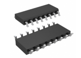
4. Packaging
SOIC16
5. Pin Assignment
6. Marking
©2016 Toshiba Corporation
2
2017-01-24
Rev.6.0
�74HC4538D
7. IEC Logic Symbol
8. Truth Table
X:
Don't care
©2016 Toshiba Corporation
3
2017-01-24
Rev.6.0
�74HC4538D
9. Block Diagram
(1)
CX, RX, DX are external
Capacitor, resistor, and diode, respectively.
(2)
External clamping diode, DX;
The external capacitor is charged to VCC level in the wait state, i.e. when no trigger is applied. Supply
voltage is turned off and CX is discharged mainly through the internal (parasitic) diode. If CX is
sufficiently large and VCC drops rapidly, there will be some possibility of damaging the IC by rush
current or latch-up. If the capacitance of the supply voltage filter is large enough and VCC drops slowly,
the rush current is automatically limited and damage to the IC is avoided.
The maximum value of forward current through the parasitic diode is ±20 mA.
In the case of a large CX, the limitation of fall time of the supply voltage is determined as follows:
tf ≥ (VCC - 0.7) CX/20 mA
(tf is the time from the voltage supply turning off to the level of supply voltage reaching 0.4 VCC.)
In the care of a system that does not satisfy the above condition, an external clamping diode is needed to
protect the IC from rush current.
©2016 Toshiba Corporation
4
2017-01-24
Rev.6.0
�74HC4538D
10. System Diagram
11. Timing Chart
©2016 Toshiba Corporation
5
2017-01-24
Rev.6.0
�74HC4538D
12. Functional Description
(1)
Stand-by state
The external capacitor is fully charge to VCC in the stand-by state. That means, before triggering, QP
and QN transistors which are connected to the T2 node are in the off state. Two comparators that relate
to the timing of the output pulse, and two reference voltage supplies stop their operation. The total
supply current is only leakage current.
(2)
Trigger operation
Trigger operation is effective in either of the following two cases. One is the condition where the A input
is low, and the B input has a falling signal. The other, where the B input is high, and the A input has a
rising signal.
After trigger becomes effective, comparators C1 and C2 start operating, and QN is turned on. The
external capacitor discharges through QN. The voltage level at the T2 node drops. If the T2 voltage level
falls to the internal reference voltage VrefL, the output of C1 becomes low. The flip-flop is then reset and
QN turns off. At that moment C1 stops but C2 continues operating.
After QN turns off, the voltage at T2 start rising at a rate determined by the time constant of external
capacitor CX and resistor RX.
After the triggering, output Q becomes high, following some delay time of the internal F/F and gates. It
stays high even if the voltage of T2 changes from falling to rising. When T2 reaches the internal reference
voltage VrefH, the output of C2 becomes low, the output Q goes low and C2 stops its operation. That
means, after triggering, when the voltage level of T2 reaches VrefH, the IC returns to its MONOSTABLE
state.
In the case of large value of CX and RX, and ignoring the discharge time of the capacitor and internal
delays of the IC, the width of the output pulse, (twOUT), is as follows:
twOUT = 0.7 × CX × RX
(3)
Retrigger operation
When another new trigger is applied to input A or B while in the MONOSTABLE state, it is effective
only if the IC is charging CX. The voltage level of T2 then falls to VrefL level again.
Therefore the Q output stays high if the next trigger comes in before the time period set by CX and RX.
If the 2nd trigger is very close to previous trigger, such as application during the discharge cycle, the 2nd
trigger will not be effective.
The minimum time for effective 2nd trigger, trr (min), depends on VCC and CX.
(4)
Reset operation
In normal operation, CD input is held high. If CD is low, a trigger has no effect because the Q output is
held low and the trigger control F/F is reset. Also, QP turns on and CX is charged rapidly to VCC.
This means if CD input is set low, the IC goes into a wait state.
©2016 Toshiba Corporation
6
2017-01-24
Rev.6.0
�74HC4538D
13. Absolute Maximum Ratings (Note)
Characteristics
Symbol
Note
Rating
Unit
Supply voltage
VCC
-0.5 to 7.0
V
Input voltage
VIN
-0.5 to VCC + 0.5
V
VOUT
-0.5 to VCC + 0.5
V
IIK
±20
mA
Output diode current
IOK
±20
mA
Output current
IOUT
±25
mA
VCC/ground current
ICC
Power dissipation
PD
Storage temperature
Tstg
Output voltage
Input diode current
(Note 1)
±50
mA
500
mW
-65 to 150
Note:
Exceeding any of the absolute maximum ratings, even briefly, lead to deterioration in IC performance or even
destruction.
Using continuously under heavy loads (e.g. the application of high temperature/current/voltage and the
significant change in temperature, etc.) may cause this product to decrease in the reliability significantly even
if the operating conditions (i.e. operating temperature/current/voltage, etc.) are within the absolute maximum
ratings and the operating ranges.
Please design the appropriate reliability upon reviewing the Toshiba Semiconductor Reliability Handbook
(“Handling Precautions”/“Derating Concept and Methods”) and individual reliability data (i.e. reliability test report
and estimated failure rate, etc).
Note 1: PD derates linearly with -8 mW/ above 85.
14. Operating Ranges (Note)
Characteristics
Supply voltage
Input voltage
Symbol
Note
Test Condition
Rating
Unit
VCC
2.0 to 6.0
V
VIN
0 to VCC
V
Output voltage
VOUT
0 to VCC
V
Operating temperature
Topr
-40 to 125
Input rise and fall times
(CD only)
tr,tf
VCC = 4.5 V
0 to 50
µs
External capacitor
CX
(Note 1)
No limitation
F
External resistor
RX
(Note 1)
VCC = 2.0 V
≥5k
Ω
VCC ≥ 3.0 V
≥1k
Note:
The operating ranges must be maintained to ensure the normal operation of the device.
Unused inputs must be tied to either VCC or GND.
Note 1: The maximum allowable values of CX and RX are a function of leakage of capacitor CX, the leakage of
74HC4538D, and leakage due to board layout and surface resistance.
Susceptibility to externally induced noise signals may occur for RX > 1 MΩ.
©2016 Toshiba Corporation
7
2017-01-24
Rev.6.0
�74HC4538D
15. Electrical Characteristics
15.1. DC Characteristics (Unless otherwise specified, Ta = 25 )
Characteristics
High-level input voltage
Low-level input voltage
High-level output voltage
(Q, Q)
Low-level output voltage
(Q, Q)
Symbol
VIH
VIL
VOH
VOL
Test Condition
VIN = VIH or VIL
Min
Typ.
Max
Unit
2.0
1.50
V
4.5
3.15
6.0
4.20
V
2.0
0.50
V
4.5
1.35
6.0
1.80
V
2.0
1.9
2.0
V
4.5
4.4
4.5
6.0
5.9
6.0
IOH = -4 mA
4.5
4.18
4.31
IOH = -5.2 mA
6.0
5.68
5.80
IOL = 20 µA
2.0
0.0
0.1
4.5
0.0
0.1
IOH = -20 µA
VIN = VIH or VIL
VCC (V)
6.0
0.0
0.1
IOL = 4 mA
4.5
0.17
0.26
IOL = 5.2 mA
V
6.0
0.18
0.26
V
IIN
VIN = VCC or GND
6.0
±0.1
µA
T2 terminal input leakage current
IIN
VIN = VCC or GND
6.0
±0.5
µA
Quiescent supply current
ICC
VIN = VCC or GND
6.0
4.0
µA
ICC(opr) VIN = VCC or GND
T2 ext = 0.25 VCC
2.0
40
120
µA
4.5
250
350
6.0
450
600
Input leakage current
Active-state supply current
(per circuit)
©2016 Toshiba Corporation
8
2017-01-24
Rev.6.0
�74HC4538D
15.2. DC Characteristics (Unless otherwise specified, Ta = -40 to 85 )
Characteristics
High-level input voltage
Low-level input voltage
High-level output voltage
(Q, Q)
Low-level output voltage
(Q, Q)
Symbol
VIH
VIL
VOH
VOL
Test Condition
VIN = VIH or VIL
VIN = VIH or VIL
IOH = -20 µA
VCC (V)
Min
Max
Unit
2.0
1.50
V
4.5
3.15
6.0
4.20
2.0
0.50
4.5
1.35
6.0
1.80
2.0
1.9
4.5
4.4
V
V
6.0
5.9
IOH = -4 mA
4.5
4.13
IOH = -5.2 mA
6.0
5.63
IOL = 20 µA
2.0
0.1
4.5
0.1
6.0
0.1
IOL = 4 mA
4.5
0.33
IOL = 5.2 mA
6.0
0.33
V
V
Input leakage current
IIN
VIN = VCC or GND
6.0
±1.0
µA
T2 terminal input leakage current
IIN
VIN = VCC or GND
6.0
±5.0
µA
ICC
VIN = VCC or GND
6.0
40.0
µA
ICC(opr) VIN = VCC or GND
T2 ext = 0.25 VCC
2.0
160
µA
4.5
400
6.0
800
Quiescent supply current
Active-state supply current
(per circuit)
15.3. DC Characteristics (Unless otherwise specified, Ta = -40 to 125 )
Characteristics
High-level input voltage
Low-level input voltage
High-level output voltage
(Q, Q)
Low-level output voltage
(Q, Q)
Symbol
VIH
VIL
VOH
VOL
Test Condition
VIN = VIH or VIL
VIN = VIH or VIL
IOH = -20 µA
VCC (V)
Min
Max
Unit
2.0
1.50
V
4.5
3.15
6.0
4.20
2.0
0.50
4.5
1.35
6.0
1.80
2.0
1.9
4.5
4.4
6.0
5.9
IOH = -4 mA
4.5
3.7
IOH = -5.2 mA
6.0
5.2
IOL = 20 µA
2.0
0.1
4.5
0.1
6.0
0.1
IOL = 4 mA
4.5
0.4
IOL = 5.2 mA
6.0
0.4
V
V
V
Input leakage current
IIN
VIN = VCC or GND
6.0
±1.0
µA
T2 terminal input leakage current
IIN
VIN = VCC or GND
6.0
±10.0
µA
ICC
VIN = VCC or GND
6.0
80.0
µA
ICC(opr) VIN = VCC or GND
T2 ext = 0.25 VCC
2.0
160
µA
4.5
400
6.0
800
Quiescent supply current
Active-state supply current
(per circuit)
©2016 Toshiba Corporation
9
2017-01-24
Rev.6.0
�74HC4538D
15.4. Timing Requirements (Unless otherwise specified, Ta = 25 , Input: tr = tf = 6 ns)
Characteristics
Symbol
Test Condition
VCC (V)
Typ.
Limit
Unit
Minimum pulse width
(A, B)
tw(L),tw(H)
2.0
75
ns
4.5
15
6.0
13
Minimum pulse width
(CD)
tw(L)
2.0
75
4.5
15
6.0
13
2.0
25
4.5
5
Minimum removal time
Minimum retrigger time
trem
trr
RX = 1 kΩ, CX = 100 pF
RX = 1 kΩ, CX = 0.01 µF
6.0
4
2.0
60
4.5
25
6.0
20
2.0
1.8
4.5
0.8
6.0
0.7
ns
ns
ns
µs
15.5. Timing Requirements
(Unless otherwise specified, Ta = -40 to 85 , Input: tr = tf = 6 ns)
Characteristics
Minimum pulse width
(A, B)
Symbol
Test Condition
VCC (V)
Limit
Unit
tw(L),tw(H)
2.0
95
ns
4.5
19
6.0
16
2.0
95
4.5
19
6.0
16
2.0
30
4.5
6
6.0
5
Minimum pulse width
(CD)
tw(L)
Minimum removal time
trem
ns
ns
15.6. Timing Requirements
(Unless otherwise specified, Ta = -40 to 125 , Input: tr = tf = 6 ns)
Characteristics
Minimum pulse width
(A, B)
Symbol
Test Condition
VCC (V)
Limit
Unit
tw(L),tw(H)
2.0
110
ns
4.5
22
6.0
19
2.0
135
4.5
27
6.0
23
2.0
40
4.5
8
6.0
7
Minimum pulse width
(CD)
tw(L)
Minimum removal time
trem
©2016 Toshiba Corporation
10
ns
ns
2017-01-24
Rev.6.0
�74HC4538D
15.7. AC Characteristics
(Unless otherwise specified, CL = 15 pF, VCC = 5 V, Ta = 25 , Input: tr = tf = 6 ns)
Characteristics
Symbol
Test Condition
Min
Typ.
Max
Unit
Output transition time
tTLH,tTHL
Propagation delay time
(A, B - Q, Q)
tPLH,tPHL
6
12
ns
25
44
Propagation delay time
(CD - Q, Q)
tPLH,tPHL
25
44
15.8. AC Characteristics (Unless otherwise specified, CL = 50 pF, Ta = 25 , Input: tr = tf
= 6 ns)
Characteristics
Output transition time
Propagation delay time
(A, B - Q, Q)
Propagation delay time
(CD - Q, Q)
Output pulse width
Symbol
Note
Test Condition
VCC (V)
Min
Typ.
Max
Unit
2.0
30
75
ns
4.5
8
15
6.0
7
13
2.0
120
250
4.5
30
50
6.0
25
43
2.0
120
250
4.5
30
50
tTLH,tTHL
tPLH,tPHL
tPLH,tPHL
twOUT
6.0
25
43
CX = 0 F
RX = 5 kΩ (VCC
= 2.0V)
RX = 1 kΩ (VCC
= 4.5 V, 6.0 V)
2.0
540
1200
4.5
180
250
6.0
150
200
CX = 0.01 µF
RX = 10 kΩ
2.0
70
83
96
4.5
69
77
85
∆twOUT
Input capacitance
CIN
Power dissipation capacitance
CPD
(Note 1)
ns
ns
µs
6.0
69
77
85
2.0
0.73
0.79
0.85
4.5
0.71
0.75
0.79
6.0
0.71
0.75
0.79
±1
%
5
10
pF
40
pF
CX = 0.1 µF
RX = 10 kΩ
Output pulse width error between
circuits (in same package)
ns
ms
Note 1: CPD is defined as the value of the internal equivalent capacitance which is calculated from the operating current
consumption without load. Average operating current can be obtained by the equation.
ICC(opr) = CPD × VCC × fIN + ICC' × Duty/100 + ICC/2 (per circuit),
(ICC': Active supply current),
(Duty: %)
©2016 Toshiba Corporation
11
2017-01-24
Rev.6.0
�74HC4538D
15.9. AC Characteristics (Unless otherwise specified, CL = 50 pF, Ta = -40 to 85 ,
Input: tr = tf = 6 ns)
Characteristics
Output transition time
Propagation delay time
(A, B - Q, Q)
Propagation delay time
(CD - Q, Q)
Output pulse width
Symbol
Test Condition
VCC (V)
Min
Max
Unit
tTLH,tTHL
2.0
95
ns
4.5
19
6.0
16
2.0
315
4.5
63
6.0
54
2.0
315
4.5
63
tPLH,tPHL
tPLH,tPHL
twOUT
CIN
ns
6.0
54
CX = 0 F
RX = 5 kΩ (VCC = 2.0V)
RX = 1 kΩ (VCC = 4.5 V, 6.0
V)
2.0
1500
ns
4.5
320
ns
6.0
260
ns
CX = 0.01 µF
RX = 10 kΩ
2.0
70
96
µs
4.5
69
85
µs
6.0
69
85
µs
2.0
0.71
0.86
ms
4.5
0.70
0.80
ms
6.0
0.70
0.80
ms
10
pF
CX = 0.1 µF
RX = 10 kΩ
Input capacitance
ns
15.10. AC Characteristics (Unless otherwise specified, CL = 50 pF, Ta = -40 to 125 ,
Input: tr = tf = 6 ns)
Characteristics
Output transition time
Symbol
Test Condition
VCC (V)
Min
Max
Unit
tTLH,tTHL
2.0
110
ns
4.5
22
6.0
19
2.0
380
4.5
76
6.0
65
2.0
380
4.5
76
6.0
65
CX = 0 F
RX = 5 kΩ (VCC = 2.0V)
RX = 1 kΩ (VCC = 4.5 V, 6.0
V)
2.0
1500
4.5
320
6.0
260
CX = 0.01 µF
RX = 10 kΩ
2.0
70
96
4.5
69
85
Propagation delay time
(A, B - Q, Q)
tPLH,tPHL
Propagation delay time
(CD - Q, Q)
tPLH,tPHL
Output pulse width
twOUT
CX = 0.1 µF
RX = 10 kΩ
©2016 Toshiba Corporation
12
6.0
69
85
2.0
0.71
0.87
4.5
0.70
0.81
6.0
0.70
0.81
ns
ns
ns
µs
ms
2017-01-24
Rev.6.0
�74HC4538D
16. Characteristics Curves (Note)
Fig. 16.1 twOUT - CX (typ.)
Fig. 16.2 trr - VCC (typ.)
Fig. 16.3 Output Pulse Width Constant K - Supply
Voltage (typ.)
Note:
The above characteristics curves are presented for reference only and not guaranteed by production test,
unless otherwise noted.
©2016 Toshiba Corporation
13
2017-01-24
Rev.6.0
�74HC4538D
Package Dimensions
Unit: mm
Weight: 0.15 g (typ.)
Package Name(s)
Nickname: SOIC16
©2016 Toshiba Corporation
14
2017-01-24
Rev.6.0
�74HC4538D
RESTRICTIONS ON PRODUCT USE
• Toshiba Corporation, and its subsidiaries and affiliates (collectively "TOSHIBA"), reserve the right to make changes to the information
in this document, and related hardware, software and systems (collectively "Product") without notice.
• This document and any information herein may not be reproduced without prior written permission from TOSHIBA. Even with TOSHIBA's
written permission, reproduction is permissible only if reproduction is without alteration/omission.
• Though TOSHIBA works continually to improve Product's quality and reliability, Product can malfunction or fail. Customers are responsible
for complying with safety standards and for providing adequate designs and safeguards for their hardware, software and systems which
minimize risk and avoid situations in which a malfunction or failure of Product could cause loss of human life, bodily injury or damage
to property, including data loss or corruption. Before customers use the Product, create designs including the Product, or incorporate
the Product into their own applications, customers must also refer to and comply with (a) the latest versions of all relevant TOSHIBA
information, including without limitation, this document, the specifications, the data sheets and application notes for Product and the
precautions and conditions set forth in the "TOSHIBA Semiconductor Reliability Handbook" and (b) the instructions for the application
with which the Product will be used with or for. Customers are solely responsible for all aspects of their own product design or applications,
including but not limited to (a) determining the appropriateness of the use of this Product in such design or applications; (b) evaluating
and determining the applicability of any information contained in this document, or in charts, diagrams, programs, algorithms, sample
application circuits, or any other referenced documents; and (c) validating all operating parameters for such designs and applications.
TOSHIBA ASSUMES NO LIABILITY FOR CUSTOMERS' PRODUCT DESIGN OR APPLICATIONS.
• PRODUCT IS NEITHER INTENDED NOR WARRANTED FOR USE IN EQUIPMENTS OR SYSTEMS THAT REQUIRE
EXTRAORDINARILY HIGH LEVELS OF QUALITY AND/OR RELIABILITY, AND/OR A MALFUNCTION OR FAILURE OF WHICH MAY
CAUSE LOSS OF HUMAN LIFE, BODILY INJURY, SERIOUS PROPERTY DAMAGE AND/OR SERIOUS PUBLIC IMPACT
("UNINTENDED USE"). Except for specific applications as expressly stated in this document, Unintended Use includes, without limitation,
equipment used in nuclear facilities, equipment used in the aerospace industry, medical equipment, equipment used for automobiles,
trains, ships and other transportation, traffic signaling equipment, equipment used to control combustions or explosions, safety devices,
elevators and escalators, devices related to electric power, and equipment used in finance-related fields. IF YOU USE PRODUCT FOR
UNINTENDED USE, TOSHIBA ASSUMES NO LIABILITY FOR PRODUCT. For details, please contact your TOSHIBA sales
representative.
• Do not disassemble, analyze, reverse-engineer, alter, modify, translate or copy Product, whether in whole or in part.
• Product shall not be used for or incorporated into any products or systems whose manufacture, use, or sale is prohibited under any
applicable laws or regulations.
• The information contained herein is presented only as guidance for Product use. No responsibility is assumed by TOSHIBA for any
infringement of patents or any other intellectual property rights of third parties that may result from the use of Product. No license to any
intellectual property right is granted by this document, whether express or implied, by estoppel or otherwise.
• ABSENT A WRITTEN SIGNED AGREEMENT, EXCEPT AS PROVIDED IN THE RELEVANT TERMS AND CONDITIONS OF SALE
FOR PRODUCT, AND TO THE MAXIMUM EXTENT ALLOWABLE BY LAW, TOSHIBA (1) ASSUMES NO LIABILITY WHATSOEVER,
INCLUDING WITHOUT LIMITATION, INDIRECT, CONSEQUENTIAL, SPECIAL, OR INCIDENTAL DAMAGES OR LOSS, INCLUDING
WITHOUT LIMITATION, LOSS OF PROFITS, LOSS OF OPPORTUNITIES, BUSINESS INTERRUPTION AND LOSS OF DATA, AND
(2) DISCLAIMS ANY AND ALL EXPRESS OR IMPLIED WARRANTIES AND CONDITIONS RELATED TO SALE, USE OF PRODUCT,
OR INFORMATION, INCLUDING WARRANTIES OR CONDITIONS OF MERCHANTABILITY, FITNESS FOR A PARTICULAR
PURPOSE, ACCURACY OF INFORMATION, OR NONINFRINGEMENT.
• Do not use or otherwise make available Product or related software or technology for any military purposes, including without limitation,
for the design, development, use, stockpiling or manufacturing of nuclear, chemical, or biological weapons or missile technology products
(mass destruction weapons). Product and related software and technology may be controlled under the applicable export laws and
regulations including, without limitation, the Japanese Foreign Exchange and Foreign Trade Law and the U.S. Export Administration
Regulations. Export and re-export of Product or related software or technology are strictly prohibited except in compliance with all
applicable export laws and regulations.
• Please contact your TOSHIBA sales representative for details as to environmental matters such as the RoHS compatibility of Product.
Please use Product in compliance with all applicable laws and regulations that regulate the inclusion or use of controlled substances,
including without limitation, the EU RoHS Directive. TOSHIBA ASSUMES NO LIABILITY FOR DAMAGES OR LOSSES OCCURRING
AS A RESULT OF NONCOMPLIANCE WITH APPLICABLE LAWS AND REGULATIONS.
©2016 Toshiba Corporation
15
2017-01-24
Rev.6.0
�


 工商网监
湘ICP备2023018690号
工商网监
湘ICP备2023018690号