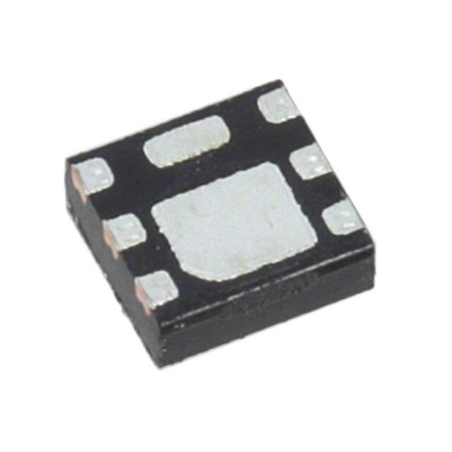
SSM6J502NU
TOSHIBA Field Effect Transistor Silicon P Channel MOS Type(U-MOSⅥ)
SSM6J502NU
Power Management Switch Applications
1.5V drive
Low ON-resistance: RDS(ON) = 60.5 mΩ (max) (@VGS = -1.5 V)
RDS(ON) = 38.4 mΩ (max) (@VGS = -1.8 V)
RDS(ON) = 28.3 mΩ (max) (@VGS = -2.5 V)
RDS(ON) = 23.1 mΩ (max) (@VGS = -4.5 V)
Unit: mm
Absolute Maximum Ratings (Ta = 25°C)
Characteristic
Symbol
Rating
Unit
Drain-Source voltage
VDSS
−20
V
Gate-Source voltage
VGSS
±8
V
ID
−6
DC
Drain current
Pulse
Power dissipation
A
−24
IDP (Note 1)
PD(Note 2)
1
W
t ≤ 10s
2
Channel temperature
Tch
150
°C
Storage temperature
Tstg
−55 to 150
°C
Note:
Using continuously under heavy loads (e.g. the application of high
temperature/current/voltage and the significant change in
temperature, etc.) may cause this product to decrease in the
reliability significantly even if the operating conditions (i.e. operating
temperature/current/voltage, etc.) are within the absolute maximum
ratings.
Please design the appropriate reliability upon reviewing the Toshiba
Semiconductor Reliability Handbook (“Handling
Precautions”/“Derating Concept and Methods”) and individual
reliability data (i.e. reliability test report and estimated failure rate,
etc).
1,2,5,6: Drain
3: Gate
4: Source
UDFN6B
JEDEC
―
JEITA
―
TOSHIBA
2-2AA1A
Weight: 8.5 mg (typ.)
Note 1: Ensure that the channel temperature does not exceed 150℃
Note 2: Mounted on FR4 board.
(25.4 mm 25.4 mm 1.6 mm, Cu Pad: 645 mm2)
Marking(Top View)
6
5
Equivalent Circuit(Top View)
4
6
5
Pin Condition(Top View)
4
6
5
4
SP2
Drain
1
2
Source
1
3
1
2
2
3
3
Polarity marking
Polarity marking (on the top)
*Electrodes : on the bottom
Start of commercial production
2010-11
© 2019
Toshiba Electronic Devices & Storage Corporation
1
2019-06-27
�SSM6J502NU
Electrical Characteristics (Ta = 25°C)
Characteristic
Symbol
Drain-Source breakdown voltage
Test Conditions
V (BR) DSS
ID = -1 mA, VGS = 0 V
V (BR) DSX
ID = -1 mA, VGS = 5 V
(Note 4)
Min
Typ.
Max
-20
―
―
-15
―
―
Unit
V
Drain cut-off current
IDSS
VDS = -20 V, VGS = 0 V
―
―
-1
μA
Gate leakage current
IGSS
VGS = ±8 V, VDS = 0 V
―
―
±1
μA
Gate threshold voltage
Vth
VDS = -3 V, ID = -1 mA
-0.3
―
-1.0
V
Forward transfer admittance
|Yfs|
VDS = -3 V, ID = -2.0 A
(Note 3)
8.8
17.5
―
S
ID = -4.0 A, VGS = -4.5 V
(Note 3)
―
18.2
23.1
ID = -4.0 A, VGS = -2.5 V
(Note 3)
―
21.5
28.3
ID = -2.5 A, VGS = -1.8 V
(Note 3)
―
26.1
38.4
ID = -1.5 A, VGS = -1.5 V
(Note 3)
―
29.7
60.5
―
1800
―
―
205
―
―
190
―
―
24.8
―
―
0.8
―
―
6.8
―
―
25
―
―
133
―
―
0.7
1.2
Drain–source ON-resistance
RDS (ON)
Input capacitance
Ciss
Output capacitance
Coss
Reverse transfer capacitance
Crss
Total Gate Charge
Qg
Gate-Source Charge
Qgs1
Gate-Drain Charge
Qgd
Switching time
VDS = -10 V, VGS = 0 V, f = 1 MHz
Turn-on time
ton
Turn-off time
toff
VDSF
Drain-Source forward voltage
VDD = −10 V, ID = −4.4 A
VGS = −4.5 V
VDD = -10 V, ID = -1.5 A,
VGS = 0 to -2.5 V, RG = 4.7 Ω
ID = 4 A, VGS = 0 V
(Note 3)
mΩ
pF
nC
ns
V
Note 3: Pulse measurement.
Note 4: If a forward bias is applied between gate and source, this device enters V (BR)DSX mode.
Note that the drain-source breakdown voltage is lowered in this mode.
Switching Time Test Circuit
(a) Test circuit
(b) VIN
0
OUT
−2.5 V
V
RG
IN
10 μs
0V
90%
VDD = −10 V
RG = 4.7 Ω
Duty ≤ 1%
VIN: tr, tf 5 ns
Common source
Ta = 25°C
10%
−2.5 V
VDS (ON)
90%
(c) Vout
10%
VDD
VDD
tr
ton
tf
toff
Precaution
Let Vth be the voltage applied between gate and source that causes the drain current (ID) to below (-1 mA for the SSM6J502NU).
Then, for normal switching operation, VGS(on) must be higher than Vth, and VGS(off) must be lower than Vth. This relationship can
be expressed as: VGS(off) < Vth < VGS(on).
Take this into consideration when using the device.
Handling Precaution
When handling individual devices that are not yet mounted on a circuit board, make sure that the environment is protected
against electrostatic discharge. Operators should wear antistatic clothing, and containers and other objects that come into direct
contact with devices should be made of antistatic materials.
Thermal resistance Rth (ch-a) and power dissipation PD vary depending on board material, board area, board thickness and pad
area. When using this device, please take heat dissipation into consideration
© 2019
Toshiba Electronic Devices & Storage Corporation
2
2019-06-27
�SSM6J502NU
ID – VDS
-10
-1.8 V
-8V
Drain current
-4.0
-2.0
Common Source
Ta = 25 °C
Pulse test
0
-0.2
ID (A)
-1
ID (A)
-4.5V
-2.5V
-6.0
0
Common Source
VDS = -3 V
Pulse test
VGS = -1.2 V
-1.5 V
-8.0
Drain current
ID – VGS
-10
-0.4
-0.6
-0.8
Drain–source voltage VDS
-0.1
Ta = 100 °C
- 25 °C
-0.01
25 °C
-0.001
-0.0001
0
-1
-0.5
Gate–source voltage VGS
(V)
ID = -4.0A
Common Source
Pulse test
25 °C
Ta = 100 °C
- 25 °C
-2
-4
-6
Gate–source voltage VGS
Drain–source ON-resistance
RDS (ON) (mΩ)
Drain–source ON-resistance
RDS (ON) (mΩ)
100
50
00
50
-2.5 V
-1.5 V
-1.8V
VGS = -4.5 V
0
-8
Common Source
Ta = 25°C
Pulse test
0
-2.0
-4.0
-1.5 A / -1.5 V
-4.0 A / -2.5 V
ID = -4.0 A / VGS = -4.5 V
0
−50
0
50
100
Gate threshold voltage Vth (V)
Drain–source ON-resistance
RDS (ON) (mΩ)
-2.5 A / -1.8V
-8.0
-10
ID (A)
Vth – Ta
-1.0
Common Source
Pulse test
50
-6.0
Drain current
(V)
RDS (ON) – Ta
100
(V)
RDS (ON) – ID
RDS (ON) – VGS
100
-1.5
-1.0
0
50
100
150
Ambient temperature Ta (°C)
Ambient temperature Ta (°C)
© 2019
Toshiba Electronic Devices & Storage Corporation
-0.5
0
−50
150
Common Source
VDS = -3 V
ID = -1 mA
3
2019-06-27
�SSM6J502NU
10
Drain reverse current IDR
30
(A)
Common Source
VDS = -3 V
Ta = 25°C
Pulse test
(S)
Forward transfer admittance |Yfs|
IDR – VDS
|Yfs| – ID
100
10
3
1
0.3
0.1
-0.01
-1
-0.1
Drain current
25 °C
Ta =100 °C
0.1
Common Source
VGS = 0 V
Pulse test
D
0.01
-25 °C
-10
0.2
ID (A)
0.4
0.6
0.8
1.0
Drain–source voltage VDS
tf
1000
(ns)
Ciss
(V)
Common Source
VDD = -10 V
VGS = 0 to -2.5 V
Ta = 25 °C
RG = 4.7Ω
toff
3000
1.2
t – ID
10000
5000
1000
500
Switching time t
Capacitance C (pF)
IDR
G
S
0.001
0
C – VDS
10000
1
300
Coss
Crss
100
50
Common Source
Ta = 25°C
f = 1 MHz
VGS = 0 V
30
10
-0.1
-1
-10
Drain–source voltage VDS
100
ton
10
tr
1
-0.001
-100
(V)
-0.01
-0.1
Drain current
-1
-10
ID (A)
Dynamic Input Characteristic
-8
Gate–source voltage VGS
(V)
Common Source
ID = -4.4 A
Ta = 25°C
-6
-4
VDD = - 10 V
VDD = - 16 V
-2
0
0
10
20
30
Total Gate Charge
40
50
Qg (nC)
© 2019
Toshiba Electronic Devices & Storage Corporation
4
2019-06-27
�SSM6J502NU
P D – Ta
1400 a: Mounted on FR4 board
1000
(25.4mm × 25.4mm × 1.6mm , Cu Pad : 645 mm2)
b: Mounted on FR4 board
(25.4mm × 25.4mm × 1.6mm , Cu Pad : 2.27mm2 )
1200
b
Power dissipation PD (mW)
Transient thermal impedance
Rth (°C/W)
Rth – Tw
100
a
10
1
0.001
Single pulse
a. Mounted on F4 board
(25.4 mm 25.4 mm 1.6 mm, Cu Pad: 645 mm2)
b. Mounted on F4 board
(25.4 mm 25.4 mm 1.6 mm, Cu Pad: 2.27 mm2)
0.01
0.1
1
Pulse width
10
tw
100
1000
a
800
600
b
400
200
0
-40
1000
-20
0
20
40
60
80
100
120 140
160
Ambient temperature Ta (°C)
(s)
Note: The above characteristics curves are presented for reference only and not guaranteed by production test, unless
otherwise noted.
© 2019
Toshiba Electronic Devices & Storage Corporation
5
2019-06-27
�SSM6J502NU
RESTRICTIONS ON PRODUCT USE
Toshiba Corporation and its subsidiaries and affiliates are collectively referred to as “TOSHIBA”.
Hardware, software and systems described in this document are collectively referred to as “Product”.
TOSHIBA reserves the right to make changes to the information in this document and related Product without notice.
This document and any information herein may not be reproduced without prior written permission from TOSHIBA. Even with TOSHIBA's
written permission, reproduction is permissible only if reproduction is without alteration/omission.
Though TOSHIBA works continually to improve Product's quality and reliability, Product can malfunction or fail. Customers are responsible for
complying with safety standards and for providing adequate designs and safeguards for their hardware, software and systems which
minimize risk and avoid situations in which a malfunction or failure of Product could cause loss of human life, bodily injury or damage to
property, including data loss or corruption. Before customers use the Product, create designs including the Product, or incorporate the
Product into their own applications, customers must also refer to and comply with (a) the latest versions of all relevant TOSHIBA information,
including without limitation, this document, the specifications, the data sheets and application notes for Product and the precautions and
conditions set forth in the "TOSHIBA Semiconductor Reliability Handbook" and (b) the instructions for the application with which the Product
will be used with or for. Customers are solely responsible for all aspects of their own product design or applications, including but not limited
to (a) determining the appropriateness of the use of this Product in such design or applications; (b) evaluating and determining the
applicability of any information contained in this document, or in charts, diagrams, programs, algorithms, sample application circuits, or any
other referenced documents; and (c) validating all operating parameters for such designs and applications. TOSHIBA ASSUMES NO
LIABILITY FOR CUSTOMERS' PRODUCT DESIGN OR APPLICATIONS.
PRODUCT IS NEITHER INTENDED NOR WARRANTED FOR USE IN EQUIPMENTS OR SYSTEMS THAT REQUIRE
EXTRAORDINARILY HIGH LEVELS OF QUALITY AND/OR RELIABILITY, AND/OR A MALFUNCTION OR FAILURE OF WHICH MAY
CAUSE LOSS OF HUMAN LIFE, BODILY INJURY, SERIOUS PROPERTY DAMAGE AND/OR SERIOUS PUBLIC IMPACT
("UNINTENDED USE"). Except for specific applications as expressly stated in this document, Unintended Use includes, without limitation,
equipment used in nuclear facilities, equipment used in the aerospace industry, lifesaving and/or life supporting medical equipment,
equipment used for automobiles, trains, ships and other transportation, traffic signaling equipment, equipment used to control combustions or
explosions, safety devices, elevators and escalators, and devices related to power plant. IF YOU USE PRODUCT FOR UNINTENDED USE,
TOSHIBA ASSUMES NO LIABILITY FOR PRODUCT. For details, please contact your TOSHIBA sales representative or contact us via our
website.
Do not disassemble, analyze, reverse-engineer, alter, modify, translate or copy Product, whether in whole or in part.
Product shall not be used for or incorporated into any products or systems whose manufacture, use, or sale is prohibited under any
applicable laws or regulations.
The information contained herein is presented only as guidance for Product use. No responsibility is assumed by TOSHIBA for any
infringement of patents or any other intellectual property rights of third parties that may result from the use of Product. No license to any
intellectual property right is granted by this document, whether express or implied, by estoppel or otherwise.
ABSENT A WRITTEN SIGNED AGREEMENT, EXCEPT AS PROVIDED IN THE RELEVANT TERMS AND CONDITIONS OF SALE FOR
PRODUCT, AND TO THE MAXIMUM EXTENT ALLOWABLE BY LAW, TOSHIBA (1) ASSUMES NO LIABILITY WHATSOEVER,
INCLUDING WITHOUT LIMITATION, INDIRECT, CONSEQUENTIAL, SPECIAL, OR INCIDENTAL DAMAGES OR LOSS, INCLUDING
WITHOUT LIMITATION, LOSS OF PROFITS, LOSS OF OPPORTUNITIES, BUSINESS INTERRUPTION AND LOSS OF DATA, AND (2)
DISCLAIMS ANY AND ALL EXPRESS OR IMPLIED WARRANTIES AND CONDITIONS RELATED TO SALE, USE OF PRODUCT, OR
INFORMATION, INCLUDING WARRANTIES OR CONDITIONS OF MERCHANTABILITY, FITNESS FOR A PARTICULAR PURPOSE,
ACCURACY OF INFORMATION, OR NONINFRINGEMENT.
Do not use or otherwise make available Product or related software or technology for any military purposes, including without limitation, for
the design, development, use, stockpiling or manufacturing of nuclear, chemical, or biological weapons or missile technology products (mass
destruction weapons). Product and related software and technology may be controlled under the applicable export laws and regulations
including, without limitation, the Japanese Foreign Exchange and Foreign Trade Law and the U.S. Export Administration Regulations. Export
and re-export of Product or related software or technology are strictly prohibited except in compliance with all applicable export laws and
regulations.
Please contact your TOSHIBA sales representative for details as to environmental matters such as the RoHS compatibility of Product. Please
use Product in compliance with all applicable laws and regulations that regulate the inclusion or use of controlled substances, including
without limitation, the EU RoHS Directive. TOSHIBA ASSUMES NO LIABILITY FOR DAMAGES OR LOSSES OCCURRING AS A RESULT
OF NONCOMPLIANCE WITH APPLICABLE LAWS AND REGULATIONS.
https://toshiba.semicon-storage.com/
© 2019
Toshiba Electronic Devices & Storage Corporation
6
2019-06-27
�