TAR5S15~TAR5S50
TOSHIBA Bipolar Linear Integrated Circuit
Silicon Monolithic
TAR5S15~TAR5S50
Point Regulators (Low-Dropout Regulator)
The TAR5Sxx Series is comprised of general-purpose bipolar single-power-supply devices incorporating a
control pin which can be used to turn them ON/OFF.
Overtemperature and overcurrent protection circuits are built
in to the devices’ output circuit.
Features
•
Low stand-by current
•
Overtemperature/overcurrent protection
•
Operation voltage range is wide.
•
Maximum output current is high.
•
Difference between input voltage and output voltage is low.
•
Small package.
•
Ceramic capacitors can be used.
Weight: 0.014 g (typ.)
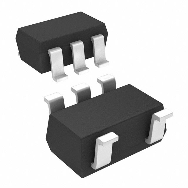
Pin Assignments (top view)
VIN
VOUT
5
4
1
2
CONTROL GND
3
NOISE
Overtemperature protection and overcurrent protection functions are not necessary guarantee of operating
ratings below the absolute maximum ratings.
Do not use devices under conditions in which their absolute maximum ratings will be exceeded.
1
2007-11-01
�TAR5S15~TAR5S50
List of Products Number and Marking
Marking on the Product
Products No.
Marking
Products No.
Marking
TAR5S15
1V5
TAR5S33
3V3
TAR5S16
1V6
TAR5S34
3V4
TAR5S17
1V7
TAR5S35
3V5
TAR5S18
1V8
TAR5S36
3V6
TAR5S19
1V9
TAR5S37
3V7
TAR5S20
2V0
TAR5S38
3V8
TAR5S21
2V1
TAR5S39
3V9
TAR5S22
2V2
TAR5S40
4V0
TAR5S23
2V3
TAR5S41
4V1
TAR5S24
2V4
TAR5S42
4V2
TAR5S25
2V5
TAR5S43
4V3
TAR5S26
2V6
TAR5S44
4V4
TAR5S27
2V7
TAR5S45
4V5
TAR5S28
2V8
TAR5S46
4V6
TAR5S29
2V9
TAR5S47
4V7
TAR5S30
3V0
TAR5S48
4V8
TAR5S31
3V1
TAR5S49
4V9
TAR5S32
3V2
TAR5S50
5V0
Example: TAR5S30 (3.0 V output)
3V0
Absolute Maximum Ratings (Ta = 25°C)
Characteristics
Symbol
Rating
Unit
Supply voltage
VIN
15
V
Output current
IOUT
200
mA
Power dissipation
PD
200
(Note 1)
380
(Note 2)
mW
Operation temperature range
Topr
−40 to 85
°C
Storage temperature range
Tstg
−55 to 150
°C
Note:
Using continuously under heavy loads (e.g. the application of high temperature/current/voltage and the
significant change in temperature, etc.) may cause this product to decrease in the reliability significantly
even if the operating conditions (i.e. operating temperature/current/voltage, etc.) are within the absolute
maximum ratings and the operating ranges.
Please design the appropriate reliability upon reviewing the Toshiba Semiconductor Reliability Handbook
(“Handling Precautions”/“Derating Concept and Methods”) and individual reliability data (i.e. reliability test
report and estimated failure rate, etc).
Note 1: Unit Ratintg
2
Note 2: Mounted on a glass epoxy circuit board of 30 × 30 mm. Pad dimension of 50 mm
2
2007-11-01
�TAR5S15~TAR5S50
TAR5S15~TAR5S22
Electrical Characteristic (unless otherwise specified, VIN = VOUT + 1 V, IOUT = 50 mA,
CIN = 1 μF, COUT = 10 μF, CNOISE = 0.01 μF, Tj = 25°C)
Characteristics
Output voltage
Symbol
Test Condition
VOUT
Min
Typ.
Max
Unit
Please refer to the Output Voltage Accuracy table.
Line regulation
Reg・line
VOUT + 1 V <
= VIN <
= 15 V,
IOUT = 1 mA
Load regulation
Reg・load
1 mA <
= IOUT <
= 150 mA
⎯
25
75
IB1
IOUT = 0 mA
⎯
170
⎯
IB2
IOUT = 50 mA
⎯
550
850
VCT = 0 V
⎯
⎯
0.1
μA
⎯
30
⎯
μVrms
Quiescent current
Stand-by current
IB (OFF)
Output noise voltage
VNO
VIN = VOUT + 1 V, IOUT = 10 mA,
10 Hz <
=f<
= 100 kHz,
CNOISE = 0.01 μF, Ta = 25°C
Temperature coefficient
TCVO
−40°C <
= Topr <
= 85°C
Input voltage
VIN
Ripple rejection
R.R.
⎯
VIN = VOUT + 1 V, IOUT = 10 mA,
CNOISE = 0.01 μF, f = 1 kHz,
VRipple = 500 mVp-p, Ta = 25°C
⎯
3
15
mV
mV
μA
⎯
100
⎯
ppm/°C
2.4
⎯
15
V
⎯
70
⎯
dB
Control voltage (ON)
VCT (ON)
⎯
1.5
⎯
VIN
V
Control voltage (OFF)
VCT (OFF)
⎯
⎯
⎯
0.4
V
Control current (ON)
ICT (ON)
VCT = 1.5 V
⎯
3
10
μA
Control current (OFF)
ICT (OFF)
VCT = 0 V
⎯
0
0.1
μA
TAR5S23~TAR5S50
Electrical Characteristic (unless otherwise specified, VIN = VOUT + 1 V, IOUT = 50 mA,
CIN = 1 μF, COUT = 10 μF, CNOISE = 0.01 μF, Tj = 25°C)
Characteristics
Symbol
Test Condition
Min
Typ.
Max
Unit
Output voltage
VOUT
Line regulation
Reg・line
VOUT + 1 V <
= VIN <
= 15 V,
IOUT = 1 mA
⎯
3
15
mV
Load regulation
Reg・load
1 mA <
= IOUT <
= 150 mA
⎯
25
75
mV
IB1
IOUT = 0 mA
⎯
170
⎯
IB2
IOUT = 50 mA
⎯
550
850
Quiescent current
Stand-by current
Output noise voltage
Dropout volatge
Temperature coefficient
IB (OFF)
VNO
VIN − VOUT
TCVO
Input voltage
VIN
Ripple rejection
R.R.
Please refer to the Output Voltage Accuracy table.
μA
VCT = 0 V
⎯
⎯
0.1
μA
VIN = VOUT + 1 V, IOUT = 10 mA,
10 Hz <
=f<
= 100 kHz,
CNOISE = 0.01 μF, Ta = 25°C
⎯
30
⎯
μVrms
IOUT = 50 mA
⎯
130
200
mV
−40°C <
= Topr <
= 85°C
⎯
100
⎯
ppm/°C
VOUT
+ 0.2 V
⎯
15
V
⎯
70
⎯
dB
⎯
VIN = VOUT + 1 V, IOUT = 10 mA,
CNOISE = 0.01 μF, f = 1 kHz,
VRipple = 500 mVp-p, Ta = 25°C
Control voltage (ON)
VCT (ON)
⎯
1.5
⎯
VIN
V
Control voltage (OFF)
VCT (OFF)
⎯
⎯
⎯
0.4
V
Control current (ON)
ICT (ON)
VCT = 1.5 V
⎯
3
10
μA
Control current (OFF)
ICT (OFF)
VCT = 0 V
⎯
0
0.1
μA
3
2007-11-01
�TAR5S15~TAR5S50
Output Voltage Accuracy
(VIN = VOUT + 1 V, IOUT = 50 mA, CIN = 1 μF, COUT = 10 μF, CNOISE = 0.01 μF, Tj = 25°C)
Product No.
Min
Typ.
Max
TAR5S15
1.44
1.5
1.56
TAR5S16
1.54
1.6
1.66
TAR5S17
1.64
1.7
1.76
TAR5S18
1.74
1.8
1.86
TAR5S19
1.84
1.9
1.96
TAR5S20
1.94
2.0
2.06
TAR5S21
2.04
2.1
2.16
TAR5S22
2.14
2.2
2.26
TAR5S23
2.24
2.3
2.36
TAR5S24
2.34
2.4
2.46
TAR5S25
2.43
2.5
2.57
TAR5S26
2.53
2.6
2.67
TAR5S27
2.63
2.7
2.77
TAR5S28
2.73
2.8
2.87
TAR5S29
2.83
2.9
2.97
TAR5S30
2.92
3.0
3.08
TAR5S31
3.02
3.1
3.18
3.12
3.2
3.28
TAR5S33
3.21
3.3
3.39
TAR5S34
3.31
3.4
3.49
TAR5S35
3.41
3.5
3.59
TAR5S36
3.51
3.6
3.69
TAR5S37
3.6
3.7
3.8
TAR5S38
3.7
3.8
3.9
TAR5S39
3.8
3.9
4.0
TAR5S40
3.9
4.0
4.1
TAR5S41
3.99
4.1
4.21
TAR5S42
4.09
4.2
4.31
TAR5S43
4.19
4.3
4.41
TAR5S44
4.29
4.4
4.51
TAR5S45
4.38
4.5
4.62
TAR5S46
4.48
4.6
4.72
TAR5S47
4.58
4.7
4.82
TAR5S48
4.68
4.8
4.92
TAR5S49
4.77
4.9
5.03
TAR5S50
4.87
5.0
5.13
TAR5S32
Symbol
VOUT
4
Unit
V
2007-11-01
�TAR5S15~TAR5S50
Application Note
1. Recommended Application Circuit
VIN
1 μF
10 μF
VOUT
5
2
Control Level
Operation
HIGH
ON
LOW
OFF
3
0.01 μF
1
4
CONTROL GND
NOISE
The figure above shows the recommended configuration for using a point regulator. Insert a capacitor for
stable input/output operation. If the control function is not to be used, Toshiba recommend that the control pin
(pin 1) be connected to the VCC pin.
2. Power Dissipation
The power dissipation for board-mounted TAR5Sxx Series devices (rated at 380 mW) is measured using a
board whose size and pattern are as shown below. When incorporating a device belonging to this series into
your design, derate the power dissipation as far as possible by reducing the levels of parameters such as input
voltage, output current and ambient temperature. Toshiba recommend that these devices should typically be
derated to 70%~80% of their absolute maximum power dissipation value.
Thermal Resistance Evaluation Board
VIN
CIN
VOUT
COUT
CNOISE
Circuit board material: glass epoxy,
Circuit board dimension:30 mm × 30 mm,
CONTROL GND
NOISE
2
Copper foil pad area: 50 mm (t = 0.8 mm)
5
2007-11-01
�TAR5S15~TAR5S50
3. Ripple Rejection
The devices of the TAR5Sxx Series feature a circuit with an excellent ripple rejection characteristic. Because
the circuit also features an excellent output fluctuation characteristic for sudden supply voltage drops, the
circuit is ideal for use in the RF blocks incorporated in all mobile telephones.
Ripple Rejection − f
TAR5S28 Input Transient Response
80
Ripple rejection (dB)
70
10 μF
60
Input voltage
3.4 V
50
2.2 μF
40
3.1 V
1 μF
2.8 V
Output voltage
30
20
10
0
10
100
VIN = 4.0 V, CNOISE = 0.01 μF,
Ta = 25°C, CIN = 1 μF,
CIN = 1 μF, Vripple = 500 mVp−p,
Iout = 10 mA, Ta = 25°C
Cout = 10 μF, CNOISE = 0.01 μF,
VIN: 3.4 V → 3.1 V, Iout = 50 mA
1k
10 k
Frequency f
0
100 k 300 k
1
2
3
(Hz)
4
5
6
7
8
9
10
Time t (ms)
4. NOISE Pin
TAR5Sxx Series devices incorporate a NOISE pin to reduce output noise voltage. Inserting a capacitor
between the NOISE pin and GND reduces output noise. To ensure stable operation, insert a capacitor of
0.0047 μF or more between the NOISE pin and GND.
The output voltage rise time varies according to the capacitance of the capacitor connected to the NOISE
pin.
CNOISE − VN
Turn On Waveform
2
CIN = 1 μF, Cout = 10 μF,
Iout = 10 mA, Ta = 25°C
Control voltage
VCT (ON) (V)
50
Control voltage waveform
40
30
20
TAR5S50
TAR5S30
10
0
0.001 μ
1
0
CNOISE = 0.01 μF
3
Output voltage
VOUT (V)
Output noise voltage VN (μV)
60
TAR5S15
0.01 μ
0.1 μ
NOISE capacitance CNOISE (F)
1 μF
2
0.33 μF
0.1 μF
1
0
−10
1.0 μ
Output voltage waveform
CIN = 1 μF, Cout = 10 μF,
Iout = 50 mA, Ta = 25°C
0
10
20
30
40
50
60
70
80
90
Time t (ms)
6
2007-11-01
�TAR5S15~TAR5S50
5. Example of Characteristics when Ceramic Capacitor is Used
Shown below is the stable operation area, where the output voltage does not oscillate, evaluated using a
Toshiba evaluation circuit. The equivalent series resistance (ESR) of the output capacitor and output current
determines this area. TAR5Sxx Series devices operate stably even when a ceramic capacitor is used as the
output capacitor.
If a ceramic capacitor is used as the output capacitor and the ripple frequency is 30 kHz or more, the ripple
rejection differs from that when a tantalum capacitor is used. This is shown below.
Toshiba recommend that users check that devices operate stably under the intended conditions of use.
Examples of safe operating area characteristics
(TAR5S15) Stable Operating Area
(TAR5S50) Stable Operating Area
100
Equivalent series resistance ESR (Ω)
Equivalent series resistance ESR (Ω)
100
10
1
Stable Operating Area
@VIN = 2.5 V, CNOISE = 0.01 μF,
0.1
CIN = 1 μF, Cout = 1 μF~10 μF,
Ta = 25°C
0.02
0
20
40
60
80
Output current
100
IOUT
120
10
Stable Operating Area
1
CIN = 1 μF, Cout = 1 μF~10 μF,
Ta = 25°C
0.02
0
140 150
@VIN = 6.0 V, CNOISE = 0.01 μF,
0.1
(mA)
20
40
60
80
Output current
100
IOUT
120
140 150
(mA)
(TAR5S28) Stable Operating Area
Evaluation Circuit for Stable Operating Area
Equivalent series resistance ESR (Ω)
100
CONTROL
10
CNOISE = 0.01 μF
TAR5S**
Stable Operating Area
VIN = VOUT
+1V
1
CIN
Ceramic
GND
COUT
Ceramic
ROUT
ESR
@VIN = 3.8 V, CNOISE = 0.01 μF,
0.1
CIN = 1 μF, Cout = 1 μF~10 μF,
Ta = 25°C
0.02
0
20
40
60
80
Output current
100
IOUT
120
140 150
Capacitors used for evaluation
Made by Murata CIN: GRM40B105K
COUT: GRM40B105K/GRM40B106K
(mA)
Ripple Rejection Characteristic (f = 10 kHz~300 kHz)
(TAR5S30)
Ripple Rejection – f
70
Ceramic 10 μF
Tantalum10 μF
Ripple rejection (dB)
60
Ceramic
2.2 μF
Ceramic
1 μF
50
40
Tantalum 2.2 μF
Tantalum 1 μF
30
20
@VIN = 4.0 V, CNOISE = 0.01 μF,
10
0
10 k
CIN = 1 μF, Vripple = 500 mVp-p,
Iout = 10 mA, Ta = 25°C
100 k
Frequency f
300 k
1000 k
(Hz)
7
2007-11-01
�TAR5S15~TAR5S50
(TAR5S15)
IOUT – VOUT
(TAR5S18)
VIN = 2.5 V, CIN = 1 μF, COUT = 10 μF,
VIN = 2.8 V, CIN = 1 μF, COUT = 10 μF,
CNOISE = 0.01 μF, Pulse width = 1 ms
CNOISE = 0.01 μF, Pulse width = 1 ms
Ta = 85°C
25
1.5
−40
1.4
0
50
100
Output current
(TAR5S20)
IOUT
Ta = 85°C
25
1.8
−40
1.7
0
150
(mA)
50
100
Output current
IOUT – VOUT
(TAR5S21)
2.1
IOUT
150
(mA)
IOUT – VOUT
2.2
VIN = 3.0 V, CIN = 1 μF, COUT = 10 μF,
VIN = 3.1 V, CIN = 1 μF, COUT = 10 μF,
CNOISE = 0.01 μF, Pulse width = 1 ms
CNOISE = 0.01 μF, Pulse width = 1 ms
Output voltage VOUT (V)
Output voltage VOUT (V)
IOUT – VOUT
1.9
Output voltage VOUT (V)
Output voltage VOUT (V)
1.6
Ta = 85°C
2.0
25
−40
1.9
0
50
100
Output current
(TAR5S22)
IOUT
Ta = 85°C
2.1
25
−40
2.0
0
150
(mA)
50
100
Output current
IOUT – VOUT
(TAR5S23)
IOUT
150
(mA)
IOUT – VOUT
VIN = 3.2 V, CIN = 1 μF, COUT = 10 μF,
VIN = 3.3 V, CIN = 1 μF, COUT = 10 μF,
CNOISE = 0.01 μF, Pulse width = 1 ms
CNOISE = 0.01 μF, Pulse width = 1 ms
Output voltage VOUT (V)
Output voltage VOUT (V)
2.3
Ta = 85°C
2.2
25
−40
2.1
0
50
Output current
100
IOUT
Ta = 85°C
2.3
25
−40
2.2
0
150
(mA)
50
Output current
8
100
IOUT
150
(mA)
2007-11-01
�TAR5S15~TAR5S50
(TAR5S25)
IOUT – VOUT
(TAR5S27)
VIN = 2.6 V, CIN = 1 μF, COUT = 10 μF,
VIN = 3.7 V, CIN = 1 μF, COUT = 10 μF,
CNOISE = 0.01 μF, Pulse width = 1 ms
CNOISE = 0.01 μF, Pulse width = 1 ms
Ta = 85°C
2.5
25
−40
2.4
0
50
100
Output current
(TAR5S28)
IOUT
25
−40
(mA)
50
100
Output current
IOUT – VOUT
(TAR5S29)
IOUT
150
(mA)
IOUT – VOUT
3
VIN = 3.8 V, CIN = 1 μF, COUT = 10 μF,
VIN = 3.9 V, CIN = 1 μF, COUT = 10 μF,
CNOISE = 0.01 μF
CNOISE = 0.01 μF
Pulse width = 1 ms
Output voltage VOUT (V)
Output voltage VOUT (V)
Ta = 85°C
2.7
2.6
0
150
2.9
Ta = 85°C
2.8
25
−40
2.7
0
50
100
Output current
(TAR5S30)
IOUT
Ta = 85°C
25
−40
(mA)
50
100
Output current
(TAR5S31)
IOUT – VOUT
IOUT
150
(mA)
IOUT – VOUT
3.2
VIN = 4.0 V, CIN = 1 μF, COUT = 10 μF,
VIN = 4.1 V, CIN = 1 μF, COUT = 10 μF,
CNOISE = 0.01 μF
CNOISE = 0.01 μF, Pulse width = 1 ms
Output voltage VOUT (V)
Pulse width = 1 ms
Ta = 85°C
3.0
25
−40
2.9
0
Pulse width = 1 ms
2.9
2.8
0
150
3.1
Output voltage VOUT (V)
IOUT – VOUT
2.8
Output voltage VOUT (V)
Output voltage VOUT (V)
2.6
50
Output current
100
IOUT
Ta = 85°C
3.1
25
−40
3.0
0
150
(mA)
50
Output current
9
100
IOUT
150
(mA)
2007-11-01
�TAR5S15~TAR5S50
(TAR5S32)
(TAR5S33)
IOUT – VOUT
VIN = 4.3 V, CIN = 1 μF, COUT = 10 μF,
CNOISE = 0.01 μF, Pulse width = 1 ms
CNOISE = 0.01 μF, Pulse width = 1 ms
Output voltage VOUT (V)
Output voltage VOUT (V)
VIN = 4.2 V, CIN = 1 μF, COUT = 10 μF,
Ta = 85°C
3.2
25
−40
3.1
0
50
100
Output current
(TAR5S35)
IOUT
3.3
25
−40
(mA)
50
100
Output current
IOUT – VOUT
(TAR5S45)
IOUT
150
(mA)
IOUT – VOUT
4.6
VIN = 4.5 V, CIN = 1 μF, COUT = 10 μF,
VIN = 5.5 V, CIN = 1 μF, COUT = 10 μF,
CNOISE = 0.01 μF
CNOISE = 0.01 μF, Pulse width = 1 ms
Pulse width = 1 ms
Output voltage VOUT (V)
Output voltage VOUT (V)
Ta = 85°C
3.2
0
150
3.6
Ta = 85°C
3.5
25
−40
3.4
0
50
100
Output current
(TAR5S48)
IOUT
4.5
25
−40
50
100
Output current
(mA)
IOUT – VOUT
(TAR5S50)
IOUT
150
(mA)
IOUT – VOUT
5.1
VIN = 5.8 V, CIN = 1 μF, COUT = 10 μF,
VIN = 6.0 V, CIN = 1 μF, COUT = 10 μF,
CNOISE = 0.01 μF
CNOISE = 0.01 μF
Output voltage VOUT (V)
Pulse width = 1 ms
Ta = 85°C
4.8
25
−40
4.7
0
Ta = 85°C
4.4
0
150
4.9
Output voltage 圧 VOUT (V)
IOUT – VOUT
3.4
3.3
50
Output current
100
IOUT
Ta = 85°C
5.0
25
−40
4.9
0
150
50
Output current
(mA)
10
Pulse width = 1 ms
100
IOUT
150
(mA)
2007-11-01
�TAR5S15~TAR5S50
(TAR5S15)
(TAR5S18)
IB – VIN
10
CIN = 1 μF, COUT = 10 μF, CNOISE = 0.01 μF
Pulse width = 1 ms
Bias current IB (mA)
CIN = 1 μF, COUT = 10 μF, CNOISE = 0.01 μF
Pulse width = 1 ms
Bias current IB (mA)
IB – VIN
10
5
5
IOUT = 150 mA
IOUT = 150 mA
100
100
1
50
0
0
5
10
Input voltage
(TAR5S20)
15
10
Input voltage
(TAR5S21)
IB – VIN
15
VIN (V)
IB – VIN
10
CIN = 1 μF, COUT = 10 μF, CNOISE = 0.01 μF
Pulse width = 1 ms
Bias current IB (mA)
CIN = 1 μF, COUT = 10 μF, CNOISE = 0.01 μF
Pulse width = 1 ms
Bias current IB (mA)
5
VIN (V)
10
5
5
IOUT = 150 mA
IOUT = 150 mA
100
100
50
0
0
5
(TAR5S22)
50
1
10
Input voltage
0
0
15
5
VIN (V)
(TAR5S23)
IB – VIN
15
VIN (V)
IB – VIN
10
CIN = 1 μF, COUT = 10 μF, CNOISE = 0.01 μF
Pulse width = 1 ms
Bias current IB (mA)
CIN = 1 μF, COUT = 10 μF, CNOISE = 0.01 μF
Pulse width = 1 ms
5
5
IOUT = 150 mA
IOUT = 150 mA
100
100
50
0
0
1
10
Input voltage
10
Bias current IB (mA)
1
50
0
0
5
Input voltage
10
50
1
0
0
15
VIN (V)
5
Input voltage
11
10
1
15
VIN (V)
2007-11-01
�TAR5S15~TAR5S50
IB – VIN
(TAR5S25)
10
CIN = 1 μF, COUT = 10 μF, CNOISE = 0.01 μF
Pulse width = 1 ms
Bias current IB (mA)
CIN = 1 μF, COUT = 10 μF, CNOISE = 0.01 μF
Pulse width = 1 ms
Bias current IB (mA)
IB – VIN
(TAR5S27)
10
5
5
IOUT = 150 mA
IOUT = 150 mA
100
100
50
0
0
5
1
10
Input voltage
15
15
VIN (V)
IB – VIN
(TAR5S29)
10
CIN = 1 μF, COUT = 10 μF, CNOISE = 0.01 μF
Pulse width = 1 ms
Bias current IB (mA)
CIN = 1 μF, COUT = 10 μF, CNOISE = 0.01 μF
Pulse width = 1 ms
5
5
IOUT = 150 mA
IOUT = 150 mA
100
100
50
0
0
5
(TAR5S30)
50
1
10
Input voltage
0
0
15
5
VIN (V)
IB – VIN
15
VIN (V)
IB – VIN
(TAR5S31)
10
CIN = 1 μF, COUT = 10 μF, CNOISE = 0.01 μF
Pulse width = 1 ms
Bias current IB (mA)
CIN = 1 μF, COUT = 10 μF, CNOISE = 0.01 μF
Pulse width = 1 ms
5
5
IOUT = 150 mA
IOUT = 150 mA
100
100
50
0
0
1
10
Input voltage
10
Bias current IB (mA)
10
Input voltage
10
Bias current IB (mA)
5
VIN (V)
IB – VIN
(TAR5S28)
1
50
0
0
5
Input voltage
10
50
1
0
0
15
VIN (V)
5
Input voltage
12
10
1
15
VIN (V)
2007-11-01
�TAR5S15~TAR5S50
(TAR5S32)
(TAR5S33)
IB – VIN
10
CIN = 1 μF, COUT = 10 μF, CNOISE = 0.01 μF
Pulse width = 1 ms
Bias current IB (mA)
CIN = 1 μF, COUT = 10 μF, CNOISE = 0.01 μF
Pulse width = 1 ms
Bias current IB (mA)
IB – VIN
10
5
IOUT = 150 mA
5
IOUT = 150 mA
100
100
50
0
0
5
10
Input voltage
(TAR5S35)
0
0
15
10
Input voltage
(TAR5S45)
IB – VIN
15
VIN (V)
IB – VIN
10
CIN = 1 μF, COUT = 10 μF, CNOISE = 0.01 μF
Pulse width = 1 ms
Bias current IB (mA)
CIN = 1 μF, COUT = 10 μF, CNOISE = 0.01 μF
Pulse width = 1 ms
Bias current IB (mA)
5
VIN (V)
10
5
5
IOUT = 150 mA
IOUT = 150 mA
100
100
50
0
0
5
1
10
Input voltage
50
0
0
15
VIN (V)
IB – VIN
(TAR5S48)
5
15
VIN (V)
IB – VIN
(TAR5S50)
10
CIN = 1 μF, COUT = 10 μF,
CNOISE = 0.01 μF
Pulse width = 1 ms
Pulse width = 1 ms
Bias current IB (mA)
CIN = 1 μF, COUT = 10 μF,
CNOISE = 0.01 μF
5
5
IOUT = 150 mA
IOUT = 150 mA
100
100
50
0
0
1
10
Input voltage
10
Bias current IB (mA)
1
50
1
5
Input voltage
10
1
50
0
0
15
VIN (V)
5
Input voltage
13
10
1
15
VIN (V)
2007-11-01
�TAR5S15~TAR5S50
(TAR5S15)
6
(TAR5S18)
VOUT – VIN
6
IOUT = 1 mA, CIN = 1 μF, COUT = 10 μF,
IOUT = 1 mA, CIN = 1 μF, COUT = 10 μF,
CNOISE = 0.01 μF, Pulse width = 1 ms
CNOISE = 0.01 μF, Pulse width = 1 ms
5
Output voltage VOUT (V)
Output voltage VOUT (V)
5
4
3
2
1
4
3
2
1
0
0
5
10
Input voltage
(TAR5S20)
6
0
0
15
10
Input voltage
(TAR5S21)
VOUT – VIN
6
IOUT = 1 mA, CIN = 1 μF, COUT = 10 μF,
15
VIN (V)
VOUT – VIN
IOUT = 1 mA, CIN = 1 μF, COUT = 10 μF,
CNOISE = 0.01 μF, Pulse width = 1 ms
5
Output voltage VOUT (V)
5
Output voltage VOUT (V)
5
VIN (V)
CNOISE = 0.01 μF, Pulse width = 1 ms
4
3
2
1
4
3
2
1
0
0
5
10
Input voltage
(TAR5S22)
6
0
0
15
10
Input voltage
(TAR5S23)
VOUT – VIN
6
IOUT = 1 mA, CIN = 1 μF, COUT = 10 μF,
15
VIN (V)
VOUT – VIN
IOUT = 1 mA, CIN = 1 μF, COUT = 10 μF,
CNOISE = 0.01 μF, Pulse width = 1 ms
5
Output voltage VOUT (V)
5
4
3
2
1
0
0
5
VIN (V)
CNOISE = 0.01 μF, Pulse width = 1 ms
Output voltage VOUT (V)
VOUT – VIN
4
3
2
1
5
Input voltage
10
0
0
15
VIN (V)
5
Input voltage
14
10
15
VIN (V)
2007-11-01
�TAR5S15~TAR5S50
(TAR5S25)
6
(TAR5S27)
VOUT – VIN
6
IOUT = 1 mA, CIN = 1 μF, COUT = 10 μF,
IOUT = 1 mA, CIN = 1 μF, COUT = 10 μF,
CNOISE = 0.01 μF, Pulse width = 1 ms
CNOISE = 0.01 μF, Pulse width = 1 ms
5
Output voltage VOUT (V)
Output voltage VOUT (V)
5
4
3
2
1
4
3
2
1
0
0
5
10
Input voltage
(TAR5S28)
6
0
0
15
10
Input voltage
(TAR5S29)
VOUT – VIN
6
IOUT = 1 mA, CIN = 1 μF, COUT = 10 μF,
15
VIN (V)
VOUT – VIN
IOUT = 1 mA, CIN = 1 μF, COUT = 10 μF,
CNOISE = 0.01 μF, Pulse width = 1 ms
5
Output voltage VOUT (V)
5
Output voltage VOUT (V)
5
VIN (V)
CNOISE = 0.01 μF, Pulse width = 1 ms
4
3
2
1
4
3
2
1
0
0
5
10
Input voltage
(TAR5S30)
6
0
0
15
10
Input voltage
(TAR5S31)
VOUT – VIN
6
IOUT = 1 mA, CIN = 1 μF, COUT = 10 μF,
15
VIN (V)
VOUT – VIN
IOUT = 1 mA, CIN = 1 μF, COUT = 10 μF,
CNOISE = 0.01 μF, Pulse width = 1 ms
5
Output voltage VOUT (V)
5
4
3
2
1
0
0
5
VIN (V)
CNOISE = 0.01 μF, Pulse width = 1 ms
Output voltage VOUT (V)
VOUT – VIN
4
3
2
1
5
Input voltage
10
0
0
15
VIN (V)
5
Input voltage
15
10
15
VIN (V)
2007-11-01
�TAR5S15~TAR5S50
(TAR5S32)
6
(TAR5S33)
VOUT – VIN
6
IOUT = 1 mA, CIN = 1 μF, COUT = 10 μF,
IOUT = 1 mA, CIN = 1 μF, COUT = 10 μF,
CNOISE = 0.01 μF, Pulse width = 1 ms
CNOISE = 0.01 μF, Pulse width = 1 ms
5
Output voltage VOUT (V)
Output voltage VOUT (V)
5
4
3
2
0
0
5
10
Input voltage
(TAR5S35)
3
2
0
0
15
VOUT – VIN
(TAR5S45)
6
5
5
4
3
2
10
Input voltage
(TAR5S48)
IOUT = 1 mA, CIN = 1 μF, COUT = 10 μF,
CNOISE = 0.01 μF, Pulse width = 1 ms
0
0
15
(TAR5S50)
5
Output voltage VOUT (V)
5
4
3
2
VIN (V)
VOUT – VIN
3
2
CNOISE = 0.01 μF, Pulse width = 1 ms
Input voltage
15
4
1
IOUT = 1 mA, CIN = 1 μF, COUT = 10 μF,
10
10
Input voltage
VOUT – VIN
5
5
VIN (V)
6
0
0
VOUT – VIN
2
6
1
VIN (V)
3
CNOISE = 0.01 μF, Pulse width = 1 ms
5
15
4
1
IOUT = 1 mA, CIN = 1 μF, COUT = 10 μF,
0
0
10
Input voltage
6
1
5
VIN (V)
Output voltage VOUT (V)
Output voltage VOUT (V)
4
1
1
Output voltage VOUT (V)
VOUT – VIN
IOUT = 1 mA, CIN = 1 μF, COUT = 10 μF,
CNOISE = 0.01 μF, Pulse width = 1 ms
0
0
15
VIN (V)
5
Input voltage
16
10
15
VIN (V)
2007-11-01
�TAR5S15~TAR5S50
(TAR5S15)
(TAR5S18)
VOUT – Ta
1.6
VIN = 2.5 V, CIN = 1 μF, COUT = 10 μF,
VIN = 2.8 V, CIN = 1 μF, COUT = 10 μF,
CNOISE = 0.01 μF, Pulse width = 1 ms
Output voltage VOUT (V)
Output voltage VOUT (V)
CNOISE = 0.01 μF, Pulse width = 1 ms
1.55
IOUT = 50 mA
1.5
100 150
1.45
1.4
−50
−25
0
25
50
75
1.85
IOUT = 50 mA
1.8
100 150
1.75
1.7
−50
100
Ambient temperature Ta (°C)
(TAR5S20)
−25
0
(TAR5S21)
VOUT – Ta
50
75
100
VOUT – Ta
2.2
VIN = 3.0 V, CIN = 1 μF, COUT = 10 μF,
VIN = 3.1 V, CIN = 1 μF, COUT = 10 μF,
CNOISE = 0.01 μF, Pulse width = 1 ms
Output voltage VOUT (V)
CNOISE = 0.01 μF, Pulse width = 1 ms
Output voltage VOUT (V)
25
Ambient temperature Ta (°C)
2.1
2.05
IOUT = 50 mA
2.0
150
100
1.95
1.9
−50
−25
0
25
50
75
2.15
IOUT = 50 mA
2.1
2.0
−50
100
(TAR5S22)
−25
0
(TAR5S23)
VOUT – Ta
75
100
VOUT – Ta
VIN = 3.3 V, CIN = 1 μF, COUT = 10 μF,
CNOISE = 0.01 μF, Pulse width = 1 ms
Output voltage VOUT (V)
CNOISE = 0.01 μF, Pulse width = 1 ms
2.25
2.1
−50
50
2.4
VIN = 3.2 V, CIN = 1 μF, COUT = 10 μF,
2.15
25
Ambient temperature Ta (°C)
2.3
2.2
150
100
2.05
Ambient temperature Ta (°C)
Output voltage VOUT (V)
VOUT – Ta
1.9
IOUT = 50 mA
150
100
−25
0
25
50
75
2.35
2.3
Ambient temperature Ta (°C)
150
100
2.25
2.2
−50
100
IOUT = 50 mA
−25
0
25
50
75
100
Ambient temperature Ta (°C)
17
2007-11-01
�TAR5S15~TAR5S50
(TAR5S25)
(TAR5S27)
VOUT – Ta
2.6
VIN = 3.5 V, CIN = 1 μF, COUT = 10 μF,
VIN = 3.7 V, CIN = 1 μF, COUT = 10 μF,
CNOISE = 0.01 μF, Pulse width = 1 ms
Output voltage VOUT (V)
Output voltage VOUT (V)
CNOISE = 0.01 μF, Pulse width = 1 ms
2.55
IOUT = 50 mA
2.5
100
150
2.45
2.4
−50
−25
0
25
50
75
2.75
2.7
IOUT = 50 mA
100
2.6
−50
100
(TAR5S28)
−25
0
25
50
75
100
Ambient temperature Ta (°C)
(TAR5S29)
VOUT – Ta
2.9
VOUT – Ta
3.0
VIN = 3.8 V, CIN = 1 μF, COUT = 10 μF,
VIN = 3.9 V, CIN = 1 μF, COUT = 10 μF,
Pulse width = 1 ms
CNOISE = 0.01 μF, Pulse width = 1 ms
Output voltage VOUT (V)
CNOISE = 0.01 μF
Output voltage VOUT (V)
150
2.65
Ambient temperature Ta (°C)
2.85
IOUT = 50 mA
2.8
150
100
2.75
2.7
−50
−25
0
25
50
75
2.95
IOUT = 50 mA
2.9
100
2.8
−50
100
(TAR5S30)
−25
0
(TAR5S31)
VOUT – Ta
75
100
VOUT – Ta
VIN = 4.1 V, CIN = 1 μF, COUT = 10 μF,
Pulse width = 1 ms
CNOISE = 0.01 μF, Pulse width = 1 ms
Output voltage VOUT (V)
CNOISE = 0.01 μF
3.05
2.9
−50
50
3.2
VIN = 4 V, CIN = 1 μF, COUT = 10 μF,
2.95
25
Ambient temperature Ta (°C)
3.1
3.0
150
2.85
Ambient temperature Ta (°C)
Output voltage VOUT (V)
VOUT – Ta
2.8
IOUT = 50 mA
150
100
−25
0
25
50
75
3.15
3.1
3.05
3.0
−50
100
Ambient temperature Ta (°C)
IOUT = 50 mA
150
100
−25
0
25
50
75
100
Ambient temperature Ta (°C)
18
2007-11-01
�TAR5S15~TAR5S50
(TAR5S32)
(TAR5S33)
VOUT – Ta
VIN = 4.3 V, CIN = 1 μF, COUT = 10 μF,
VIN = 4.2 V, CIN = 1 μF, COUT = 10 μF,
CNOISE = 0.01 μF, Pulse width = 1 ms
Output voltage VOUT (V)
Output voltage VOUT (V)
CNOISE = 0.01 μF, Pulse width = 1 ms
3.25
IOUT = 50 mA
3.2
3.15
150
100
3.1
−50
−25
0
25
50
75
3.35
3.3
IOUT = 50 mA
3.2
−50
100
(TAR5S35)
−25
0
(TAR5S45)
VOUT – Ta
50
75
100
VOUT – Ta
4.6
VIN = 5.5 V, CIN = 1 μF, COUT = 10 μF,
VIN = 4.5 V, CIN = 1 μF, COUT = 10 μF,
CNOISE = 0.01 μF, Pulse width = 1 ms
Output voltage VOUT (V)
CNOISE = 0.01 μF, Pulse width = 1 ms
Output voltage VOUT (V)
25
Ambient temperature Ta (°C)
3.6
3.55
IOUT = 50 mA
3.45
150
100
3.4
−50
−25
0
25
50
75
4.55
4.5
IOUT = 50 mA
4.45
150
100
4.4
−50
100
Ambient temperature Ta (°C)
(TAR5S48)
−25
0
25
50
75
100
Ambient temperature Ta (°C)
(TAR5S50)
VOUT – Ta
4.9
VOUT – Ta
5.1
VIN = 5.8 V, CIN = 1 μF, COUT = 10 μF,
VIN = 6 V, CIN = 1 μF, COUT = 10 μF,
Pulse width = 1 ms
CNOISE = 0.01 μF
Output voltage VOUT (V)
CNOISE = 0.01 μF
Output voltage VOUT (V)
150
100
3.25
Ambient temperature Ta (°C)
3.5
VOUT – Ta
3.4
3.3
4.85
4.8
IOUT = 50 mA
4.75
150
5
IOUT = 50 mA
4.95
150
100
4.7
−50
−25
Pulse width = 1 ms
5.05
100
0
25
50
75
4.9
−50
100
Ambient temperature Ta (°C)
−25
0
25
50
75
100
Ambient temperature Ta (°C)
19
2007-11-01
�TAR5S15~TAR5S50
IB – Ta
(TAR5S23~TAR5S50)
3
VIN = VOUT + 1 V, CIN = 1 μF,
COUT = 10 μF, CNOISE = 0.01 μF
Pulse width = 1 ms
IOUT = 150 mA
Dropout voltage VIN - VOUT (V)
Bias current
IB (mA)
2.5
2
1.5
100
1
50
0.5
10
0.5
CIN = 1 μF, COUT = 10 μF,
CNOISE = 0.01 μF
Pulse width = 1 ms
0.4
IOUT = 150 mA
0.3
100
0.2
50
0.1
10
1
1
0
−50
−25
0
25
50
75
0
−50
100
−25
(TAR5S23~TAR5S50)
0.4
50
75
100
IB – IOUT
2.5
CIN = 1 μF, COUT = 10 μF,
CNOISE = 0.01μF
Pulse width = 1 ms
2.0
85
Ta = 25°C
0.3
−40
0.2
0.1
VIN = VOUT + 1 V,
CIN = 1 μF, COUT = 10 μF,
CNOISE = 0.01 μF
−40
Pulse width = 1 ms
Ta = 25°C
1.5
85
1.0
0.5
0
0
50
100
Output current
IOUT
0
0
150
50
(mA)
Turn On Waveform
1
0
VIN = VOUT + 1 V,
VCT (ON) = 0 → 1.5 V, CIN = 1 μF,
COUT = 10 μF, CNOISE =
0.01 μF
Output voltage
VOUT (V)
Ta = 25°C
85
0
VIN = VOUT + 1 V,
VCT (ON) = 1.5 → 0 V, CIN = 1 μF,
2
COUT = 10 μF, CNOISE =
0.01 μF
1
Control voltage waveform
0
3
2
0
(mA)
Output voltage waveform
−40
1
Control voltage
VCT (ON) (V)
Control voltage waveform
3
IOUT
150
Turn Off Waveform
3
2
100
Output current
3
Control voltage
VCT (ON) (V)
25
VIN - VOUT – IOUT
Bias current IB (mA)
Dropout voltage VIN - VOUT (V)
0.5
0
Ambient temperature Ta (°C)
Ambient temperature Ta (°C)
Output voltage
VOUT (V)
VIN - VOUT – Ta
0.6
1
2
1
Output voltage waveform
0
0
Time t (ms)
1
Time t (ms)
20
2007-11-01
�TAR5S15~TAR5S50
Ripple Rejection – f
VN – f
80
10
TAR5S25 (2.5 V)
TAR5S30 (3.0 V)
TAR5S15 (1.5 V)
70
COUT = 10 μF, CNOISE = 0.01 μF,
10 Hz < f < 100 kHz, Ta = 25°C
1
Ripple rejection (dB)
Output noise voltage VN (μV/√ Hz )
VIN = VOUT + 1 V, IOUT = 10 mA, CIN = 1 μF,
0.1
60
50
TAR5S45 (4.5 V)
TAR5S50 (5.0 V)
40
TAR5S35 (3.5 V)
30
20
VIN = VOUT + 1 V, IOUT = 10 mA, CIN = 1 μF,
10 COUT = 10 μF, CNOISE = 0.01 μF,
VRipple = 500 mVp-p, Ta = 25°C
0
10
100
1k
10 k
100 k
0.01
0.001
10
100
1k
Frequency f
10 k
100 k
80
120
Frequency f
1000 k
(Hz)
(Hz)
PD – Ta
400
Power dissipation PD
(mW)
①
300
200
②
100
① Circuit board material: glass epoxy,
Circuit board dimention:
30 mm × 30 mm, 2
pad area: 50 mm (t = 0.8 mm)
② Unit
0
−40
0
40
Ambient temperature Ta (°C)
21
2007-11-01
�TAR5S15~TAR5S50
Package Dimensions
Weight: 0.014 g (typ.)
22
2007-11-01
�TAR5S15~TAR5S50
RESTRICTIONS ON PRODUCT USE
• Toshiba Corporation, and its subsidiaries and affiliates (collectively “TOSHIBA”), reserve the right to make changes to the information
in this document, and related hardware, software and systems (collectively “Product”) without notice.
• This document and any information herein may not be reproduced without prior written permission from TOSHIBA. Even with
TOSHIBA’s written permission, reproduction is permissible only if reproduction is without alteration/omission.
• Though TOSHIBA works continually to improve Product’s quality and reliability, Product can malfunction or fail. Customers are
responsible for complying with safety standards and for providing adequate designs and safeguards for their hardware, software and
systems which minimize risk and avoid situations in which a malfunction or failure of Product could cause loss of human life, bodily
injury or damage to property, including data loss or corruption. Before creating and producing designs and using, customers must
also refer to and comply with (a) the latest versions of all relevant TOSHIBA information, including without limitation, this document,
the specifications, the data sheets and application notes for Product and the precautions and conditions set forth in the “TOSHIBA
Semiconductor Reliability Handbook” and (b) the instructions for the application that Product will be used with or for. Customers are
solely responsible for all aspects of their own product design or applications, including but not limited to (a) determining the
appropriateness of the use of this Product in such design or applications; (b) evaluating and determining the applicability of any
information contained in this document, or in charts, diagrams, programs, algorithms, sample application circuits, or any other
referenced documents; and (c) validating all operating parameters for such designs and applications. TOSHIBA ASSUMES NO
LIABILITY FOR CUSTOMERS’ PRODUCT DESIGN OR APPLICATIONS.
• Product is intended for use in general electronics applications (e.g., computers, personal equipment, office equipment, measuring
equipment, industrial robots and home electronics appliances) or for specific applications as expressly stated in this document.
Product is neither intended nor warranted for use in equipment or systems that require extraordinarily high levels of quality and/or
reliability and/or a malfunction or failure of which may cause loss of human life, bodily injury, serious property damage or serious
public impact (“Unintended Use”). Unintended Use includes, without limitation, equipment used in nuclear facilities, equipment used
in the aerospace industry, medical equipment, equipment used for automobiles, trains, ships and other transportation, traffic signaling
equipment, equipment used to control combustions or explosions, safety devices, elevators and escalators, devices related to electric
power, and equipment used in finance-related fields. Do not use Product for Unintended Use unless specifically permitted in this
document.
• Do not disassemble, analyze, reverse-engineer, alter, modify, translate or copy Product, whether in whole or in part.
• Product shall not be used for or incorporated into any products or systems whose manufacture, use, or sale is prohibited under any
applicable laws or regulations.
• The information contained herein is presented only as guidance for Product use. No responsibility is assumed by TOSHIBA for any
infringement of patents or any other intellectual property rights of third parties that may result from the use of Product. No license to
any intellectual property right is granted by this document, whether express or implied, by estoppel or otherwise.
• ABSENT A WRITTEN SIGNED AGREEMENT, EXCEPT AS PROVIDED IN THE RELEVANT TERMS AND CONDITIONS OF SALE
FOR PRODUCT, AND TO THE MAXIMUM EXTENT ALLOWABLE BY LAW, TOSHIBA (1) ASSUMES NO LIABILITY
WHATSOEVER, INCLUDING WITHOUT LIMITATION, INDIRECT, CONSEQUENTIAL, SPECIAL, OR INCIDENTAL DAMAGES OR
LOSS, INCLUDING WITHOUT LIMITATION, LOSS OF PROFITS, LOSS OF OPPORTUNITIES, BUSINESS INTERRUPTION AND
LOSS OF DATA, AND (2) DISCLAIMS ANY AND ALL EXPRESS OR IMPLIED WARRANTIES AND CONDITIONS RELATED TO
SALE, USE OF PRODUCT, OR INFORMATION, INCLUDING WARRANTIES OR CONDITIONS OF MERCHANTABILITY, FITNESS
FOR A PARTICULAR PURPOSE, ACCURACY OF INFORMATION, OR NONINFRINGEMENT.
• Do not use or otherwise make available Product or related software or technology for any military purposes, including without
limitation, for the design, development, use, stockpiling or manufacturing of nuclear, chemical, or biological weapons or missile
technology products (mass destruction weapons). Product and related software and technology may be controlled under the
Japanese Foreign Exchange and Foreign Trade Law and the U.S. Export Administration Regulations. Export and re-export of Product
or related software or technology are strictly prohibited except in compliance with all applicable export laws and regulations.
• Please contact your TOSHIBA sales representative for details as to environmental matters such as the RoHS compatibility of Product.
Please use Product in compliance with all applicable laws and regulations that regulate the inclusion or use of controlled substances,
including without limitation, the EU RoHS Directive. TOSHIBA assumes no liability for damages or losses occurring as a result of
noncompliance with applicable laws and regulations.
23
2007-11-01
�