TB67S158FTG
TOSHIBA Bi-CD Process Integrated Circuit Silicon Monolithic
TB67S158FTG
1. Summary/Features/Appearance
Constant voltage control DMOS driver incorporating 2 function modes (full parallel input and
serial input).
FTG
Summary
The TB67S158 is a constant voltage control DMOS driver. It can operate
maximum of two unipolar stepping motors (max).
Mode1: Full parallel input (similar to transistor array)
Mode2: Serial input
Output voltage of 80V and maximum current of 1.5A are realized by
applying BiCD process. Motor can be driven by single power supply of VM
with the internal regulator.
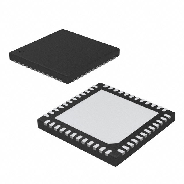
P-WQFN48-0707-0.50-003
Weight: 1.1g (typ.)
Features
・Capable of operating maximum of two 2-phase unipolar stepping motors by one chip.
・High voltage and current (as for specifications, please refer to the absolute maximum ratings and operation
ranges).
・Low on resistance (Ron=0.5Ω (typ.)) of output step is realized by BiCD process.
・Built-in VCC regulator for internal circuit control (capable of operating by only VM power supply)
・Capable of constant voltage driving (corresponding to 2-phase and 1-2-phase excitation drives)
・Built-in thermal shutdown circuit (TSD), over current detection (ISD), and power on reset of VM power
supply
・ALERT signal can be outputted to outside when thermal shutdown circuit (TSD) or over current detection
(ISD) operates
Note) Please be careful about the thermal conditions during use.
© 2014-2020
Toshiba Electronic Devices & Storage Corporation
1
2020-08-28
�TB67S158FTG
2. Block diagram: Mode1 (Full parallel mode)
IN_A1
IN_A2
IN_B1
IN_B2
MODE
Polarity and Angle
control A
Polarity and Angle
control B
Ach
Pre
Ach
OUT
drv
Nch×2
Bch
Pre
Bch
OUT
Nch×2
drv
OUT_A+
OUT_AVCOMAB
OUT_B+
OUT_B-
MODE Control
Error detect
(TSD/ISD)
Internal OSC
POR
VM
ERR
Pre TSD
VCC regulator
IN_C1
IN_C2
IN_D1
IN_D2
Polarity and Angle
control C
Polarity and Angle
control D
2
Cch
Pre
drv
Cch
OUT
Nch×2
Dch
Pre
drv
Dch
OUT
OUT_D+
Nch×2
OUT_D-
OUT_C+
OUT_CVCOMCD
2020-08-28
�TB67S158FTG
3. Pin name/ assignment: Mode1 (Full parallel mode)
LGND
MODE
NC
NC
NC
VM
NC
NC
NC
ERR
LGND
NC
(Top View)
36 35 34 33 32 31 30 29 28 27 26 25
VCOM_CD
37
24 VCOM_AB
OUT_D+
38
23 OUT_B+
OUT_D+
39
22 OUT_B+
OUT_D-
40
21 OUT_B-
OUT_D-
41
20 OUT_B-
PGND_CD
42
PGND_CD
43
18 PGND_AB
OUT_C-
44
17 OUT_A-
OUT_C-
45
16 OUT_A-
OUT_C+
46
15 OUT_A+
OUT_C+
47
14
OUT_A+
48
13
NC
IN_D1
IN_D2
IN_C1
IN_C2
IN_A1
7
8
9 10 11 12
NC
6
NC
5
IN_B2
4
IN_B1
3
IN_A2
2
NC
1
NC
NC
19 PGND_AB
TB67S158FTG
(*) Please mount the four corner pins of the QFN package and the exposed pad to the GND area of the PCB.
3
2020-08-28
�TB67S158FTG
3-1. Application Notes
1) All the grounding wires of the device must run on the solder mask on the PCB and be externally terminated at
only one point. Also, a grounding method should be considered for efficient heat dissipation.
2) When setting pin of each mode is controlled by SW, the voltage should be pull-up to the power supply which is
the same voltage of the input signal or pull-down to the GND in order to avoid Hi-Z.
3) Careful attention should be paid to the layout of the output, VM and GND traces, to avoid short circuits across
output pins or to the power supply or ground. If such a short circuit occurs, the device may be permanently
damaged.
4) Also, the utmost care should be taken for pattern designing and implementation of the device since it has power
supply pins (VM, OUT, GND, etc.) through which a particularly large current may run. If these pins are wired
incorrectly, an operation error may occur or the device may be destroyed.
The logic input pins must also be wired correctly. Otherwise, the device may be damaged owing to a current running
through the IC that is larger than the specified current.
4
2020-08-28
�TB67S158FTG
3-2. Pin assignment of the TB67S158 (QFN48)
Pin No.
Full parallel(MODE=L)
Serial/Parallel(MODE=H)
1
2
3
4
5
6
7
8
9
10
11
12
13
14
15
16
17
18
19
20
21
22
23
24
25
26
27
28
29
30
31
32
33
34
35
36
37
38
39
40
41
42
43
44
45
46
47
48
NC
IN_D1
IN_D2
IN_C1
IN_C2
IN_A1
NC
IN_A2
IN_B1
IN_B2
NC
NC
NC
OUT_A+
OUT_A+
OUT_AOUT_APGND_AB
PGND_AB
OUT_BOUT_BOUT_B+
OUT_B+
VCOM_AB
LGND
MODE
NC
NC
NC
VM
NC
NC
NC
ERR
LGND
NC
VCOM_CD
OUT_D+
OUT_D+
OUT_DOUT_DPGND_CD
PGND_CD
OUT_COUT_COUT_C+
OUT_C+
NC
NC
DATA
CLK
ALM
NC
CLR
NC
GATE
STBY
LATCH
NC
NC
NC
OUT_A+
OUT_A+
OUT_AOUT_APGND_AB
PGND_AB
OUT_BOUT_BOUT_B+
OUT_B+
VCOM_AB
LGND
MODE
NC
NC
NC
VM
NC
NC
NC
ERR
LGND
NC
VCOM_CD
OUT_D+
OUT_D+
OUT_DOUT_DPGND_CD
PGND_CD
OUT_COUT_COUT_C+
OUT_C+
NC
* NC pins should be set open.
5
2020-08-28
�TB67S158FTG
3-3. Pin description of the TB67S158 (QFN48)
Pin No.
1
2
3
4
5
6
7
8
9
10
11
12
13
14
15
16
17
18
19
20
21
22
23
24
25
26
27
28
29
30
31
32
33
34
35
36
37
38
39
40
41
42
43
44
45
46
47
48
Full parallel (MODE=L)
Serial/Parallel (MODE=H)
NC
NC
OUT_D+ ON pin
Input pin for serial data
OUT_D- ON pin
Input pin for serial clock
OUT_C+ ON pin
Output pin for rising temperature detection
OUT_C- ON pin
NC
OUT_A+ ON pin
Clear pin for storage register
NC
NC
OUT_A- ON pin
Clear pin for storage register
OUT_B+ ON pin
Standby setting pin
OUT_B- ON pin
Input pin for serial latch
NC
NC
NC
NC
NC
NC
Output + pin for phase A
Output + pin for phase A
Output + pin for phase A
Output + pin for phase A
Output - pin for phase A
Output - pin for phase A
Output - pin for phase A
Output - pin for phase A
Power ground pin
Power ground pin
Power ground pin
Power ground pin
Output - pin for phase B
Output - pin for phase B
Output - pin for phase B
Output - pin for phase B
Output + pin for phase B
Output + pin for phase B
Output + pin for phase B
Output + pin for phase B
Common pin for phase A and B
Common pin for phase A and B
LGND
Switching pin for I/F MODE
(L setting)
NC
LGND
Switching pin for I/F MODE
(H setting)
NC
NC
NC
NC
NC
Pin for main power supply
Pin for main power supply
NC
NC
NC
NC
NC
NC
Output pin for abnormal detection
Output pin for abnormal detection
Logic ground pin
Logic ground pin
NC
NC
Common pin for phase C and D
Common pin for phase C and D
Output + pin for phase D
Output + pin for phase D
Output + pin for phase D
Output + pin for phase D
Output - pin for phase D
Output - pin for phase D
Output - pin for phase D
Output - pin for phase D
Power ground pin
Power ground pin
Power ground pin
Power ground pin
Output - pin for phase C
Output - pin for phase C
Output - pin for phase C
Output - pin for phase C
Output + pin for phase C
Output + pin for phase C
Output + pin for phase C
Output + pin for phase C
NC
NC
6
2020-08-28
�TB67S158FTG
4. Functional/Operation description
4-1. Pin interface
TB67S158FTG
1kΩ
Logic
Output pin
100kΩ
Logic
Input pin
GND
GND
VCOM
OUT+
OUT-
GND
The equivalent circuit diagrams may be simplified or some parts of them may be omitted for explanatory purposes.
7
2020-08-28
�TB67S158FTG
Protection circuit
Note: Logic pin is pull-down or pull-up by the resistor of about 100 kΩ in the IC.
(Confirm the input equivalent circuit.)
Functional description
ISD (over current detection)
ISD turns off the output of the motor when it detects over current (exceeding absolute maximum rating) in the
output transistors. It is cleared when VM power supply is applied again or configured standby mode.
TSD (thermal shutdown circuit)
TSD turns off all outputs of the motor when it detects abnormal temperature (Tj =160°C (typ.)) of the IC. It is
cleared when VM power supply is applied again or configured standby mode.
VMR (VM power supply monitor) circuit
When the voltage of VM is higher than the specified value, output is set high level. When it is lower than the
specified value, output is set low (internal status).
POR (Power On Reset) circuit
When both VMR and VCCR are high: Logic transistors = active, Other states: Logic transistors = OFF
8
2020-08-28
�TB67S158FTG
5. MODE pin
MODE
Function
L
Mode1 Full parallel control I/F (Similar operation of transistor array)
H
Mode2 Serial/Parallel conversion control I/F
6. Pin function of full parallel control IF (Mode1)
IN_X pin can control each transistor directly like transistor array.
IN_A1
IN_A2
IN_B1
IN_B2
Function
L
-
-
-
OUT_A+=OFF
H
-
-
-
OUT_A+=ON
-
L
-
-
OUT_A-=OFF
-
H
-
-
OUT_A-=ON
-
-
L
-
OUT_B+=OFF
-
-
H
-
OUT_B+=ON
-
-
-
L
OUT_B-=OFF
-
-
-
H
OUT_B-=ON
IN_C1
IN_C2
IN_D1
IN_D2
Function
L
-
-
-
OUT_C+=OFF
H
-
-
-
OUT_C+=ON
-
L
-
-
OUT_C-=OFF
-
H
-
-
OUT_C-=ON
-
-
L
-
OUT_D+=OFF
-
-
H
-
OUT_D+=ON
-
-
-
L
OUT_D-=OFF
-
-
-
H
OUT_D-=ON
9
2020-08-28
�TB67S158FTG
6-1. ERR (output function of abnormal detection)
ERR output
Function
H
Normal operation
L
Abnormal detection (TSD or ISD)
ERR pin is a logic output pin of open drain type. It outputs high level (pull-up voltage level) in the normal operation.
It outputs low (GND level) when TSD or ISD operates. When TSD or ISD detection is cleared, high level is
outputted.
3.3V or 5V
10kΩ
ERR output
ERR logic
[MOSFET for ERR]
ON: When abnormal detection
operaties
OFF: In normal operation
10
2020-08-28
�TB67S158FTG
7. Pin function of serial/parallel conversion control I/F (Mode2)
7-1. Input interface (8-bit shift register + 8-bit storage register)
CLK
8-bit shift register
DATA
CLR
Qa
Qb
Qc
Qd
Qe
Qf
Qg
Qh
8-bit storage register
QB
QD
QE
QF
QG
QH
ENABLE_C-
ENABLE_C+
ENABLE_B-
ENABLE_B+
ENABLE_A-
Logic input gate
ENABLE_A+
GATE
QC
ENABLE_D-
QA
ENABLE_D+
LATCH
STBY
Motor Control Logic
* Initial value for each logic pin when signal is not inputted
Pin name
CLK
DATA
CLR
LATCH
GATE
STBY
Initial value
Low
Low
Low
Low
High
Low
Initial state for each logic pin when signal is not inputted is as follows.
LATCH: Low=sift register/storage register: initial state
GATE: High=ENABLE_X+ENABLE_X-=Disable * ”X” of ENABLE_X stands for A, B, C, and D.
STBY=Low: standby state
11
2020-08-28
�TB67S158FTG
Timing chart of input signal (normal input)
CLR
SI0
DATA
SI1
SI2
SI3
SI4
SI5
SI6
SI7
SI0
SI1
SI2
SI3
SI4
SI5
SI6
SI7
CLK
Shift
Register
Qh
Qg
Qf
Qe
Qd
Qc
Qb
Qa
Qh
Qg
Qf
Qe
Qd
Qc
Qb
QG
QF
QE
QD
QC
QB
QA
Qa
LATCH
Storage
Register
QH
GATE
Signal inputted to
logic transistors
ENB ENB ENB ENB ENB
DCC+
BD+
ENB ENB
B+
A-
ENB
A+
• Truth table
Input
Function
CLK
DATA
CLR
LATCH
GATE
X
X
X
X
L
Data of ENABLE_X+ and ENABLE_X-: Not applicable
X
X
X
X
H
Data of ENABLE_X+ and ENABLE_X-: Applicable
X
X
L
X
X
Data stored in the storage register is cleared
L
↑
H
X
X
The first step of the shift register: ’L’, Others: data of each prior step is stored.
H
↑
H
X
X
The first step of the shift register: ’H’, Others: data of each prior step is stored.
X
↓
H
X
X
Shift register keeps prior state.
X
X
H
↑
X
Data of shift register is stored in the storage register.
X
X
H
↓
X
Storage register keeps prior state.
Truth table: X=Don’t care
* ”X” of ENABLE_X stands for A, B, C, and D.
* Note: To operate logic output normally, SCK must be configured low in data transfer and complete.
• Description of logic signal
Signal name
ENABLE_X
STBY
H
L
Notes
Output ON
Output OFF
When ENABLE_x is set low, output of corresponded channel is turned off
(Hi-z).
Motor operation:
enable
Turn off all functions
of the IC
When STBY is set L, motor output is turned off. (Motor cannot operate).
12
2020-08-28
�TB67S158FTG
7-2. Function of ALM (output function of thermal shutdown alarm)
(Enable in serial/parallel conversion control I/F)
ALM output
Function
H
Normal operation
L
Thermal shutdown alarm function (Thermal_Alarm)
ALM pin is a logic output pin of open drain type. It outputs high (pull-up voltage level) in normal state.
When the temperature of the IC reaches specified threshold (Thermal_Alarm), low level (GND level) is outputted.
Function of ALM is cleared automatically when the temperature of the IC falls 30°C (target value) lower than the
threshold of Thermal Alarm.
3.3V or 5V
Threshold of ALM detection
ON: 120°C (target value)
10kΩ
ALM output
ALM logic
[MOSFET for ALM]
ON: In reaching theshold of
detection
OFF: In normal state and in
reaching threshold of
release
The equivalent circuit diagrams may be simplified or some parts of them may be omitted for explanatory purposes.
13
2020-08-28
�TB67S158FTG
8. Absolute maximum ratings (Ta=25°C)
Characteristics
Symbol
Rating
Unit
VM (max)
80
V
Motor output voltage
VOUT (max)
80
V
Motor output current
IOUT (max)
1.5
A
Internal logic power supply
VCC (max)
6.0
V
VIN (H)(max)
6.0
V
VIN (L)(min)
-0.4
V
Open drain output pin (MO,ERR,ALM) voltage range
Vod (max)
6.0
V
Open drain output pin (MO,ERR,ALM) inflow current range
Iod (max)
20
mA
Power dissipation (Note)
PD
1.3
W
Operating temperature
Topr
-20 to 85
°C
Storage temperature
Tstg
-55 to 150
°C
Junction temperature
Tj (max)
150
°C
Motor power supply VM
Logic input voltage
Note: Monolithic. When the temperature (Ta) exceeds 25°C, derate the value by 10.4mW/°C.
Ta:
Ambient temperature of the IC
Topr: Ambient temperature of the IC under operation.
Tj:
Chip temperature of the IC under operation. The maximum of Tj is limited by the temperature of TSD (thermal
shutdown circuit). It is recommended to design the IC by considering the maximum of the usage current of 120°C.
Absolute maximum ratings
The absolute maximum ratings of a semiconductor device are a set of ratings that must not be exceeded, even for
a moment. Do not exceed any of these ratings. Exceeding the rating (s) may cause device breakdown, damage or
deterioration, and may result in injury by explosion or combustion. The value of even one parameter of the absolute
maximum ratings should not be exceeded under any circumstances. The device does not have overvoltage
detection circuit. Therefore, the device is damaged if a voltage exceeding its rated maximum is applied. All voltage
ratings, including supply voltages, must always be followed. The other notes and considerations described later
should also be referred to.
14
2020-08-28
�TB67S158FTG
(For reference) Relation of power dissipation and ambient temperature
Power dissipation PD [W]
PD-Ta Graph
Ambient temperature Ta [°C]
(1) Monolithic
(2) When mounted on a 4-layer glass epoxy board (power dissipation example of
Rth(j-a)=25°C/W (when mounted); dependent of board and mount condition.)
9. Operation ranges
Characteristics
Motor power supply VM
Symbol
VM
Test condition
Min
Typ.
Max
Unit
—
10
24
60
V
Motor output voltage
VOUT
Connecting to zener (24V)
10
48
60
V
Motor output current
IOUT
Ta=25°C per phase
―
1.0
1.5
A
Internal logic power supply
VCC
―
4.75
5.0
5.25
V
VIN (H)
Logic input high level
2.0
―
5.5
V
VIN (L)
Logic input low level
0
―
0.8
V
Logic input voltage
Open drain pin voltage range
Vod (range)
ERR, ALM pin
3.0
―
5.5
V
Open drain pin inflow current range
Iod (range)
ERR, ALM pin
―
―
10
mA
(Note): Please use the device with extra margin regarding the absolute maximum ratings.
15
2020-08-28
�TB67S158FTG
10. Electrical characteristics
10-1. DC electrical specifications 1 (Ta=25°C, VM=24V, unless otherwise specified)
Characteristics
Symbol
Test condition
Min
Typ.
Max
Unit
VIH
Logic input voltage High level
2.0
―
5.5
V
VIL
Logic input voltage Low level
GND
―
0.8
V
(Note 1)
100
―
300
mV
Logic input voltage
Input hysteresis
VIN (HYS)
High
IIN (H)
Logic input voltage High level (VIN=3.3V)
―
33
55
μA
Low
IIN (L)
Logic input voltage Low level
―
―
1
μA
Output pins: open, VIN=VIL, Standby mode
―
0.7
1.0
mA
―
1.3
2.0
mA
Logic input current
IM1
IM consumption current
Output pins: open, Normal operation
IM2
Motor output steps: no operation
Open drain logic output pin voltage
VOL
IOL=5mA (output pins: Low)
―
―
0.5
V
VFN
VM=24V, IOUT=1.5A,Tj=25°C
―
1.2
―
V
―
0.5
0.7
Ω
Regenerative diode
Forward voltage
Output transistor
IOUT=1.5A
Drain-Source
RON (D-S)
Tj=25°C
On-resistance
(Note 1): VIN (H) is defined as the VIN voltage that causes the outputs to change when the voltage of the test pin is
gradually raised from 0 V. VIN (L) is defined as the VIN voltage that causes the outputs to change when the voltage of the
pin is then gradually lowered. The difference between VIN (L) and VIN (H) is defined as the input hysteresis.
16
2020-08-28
�TB67S158FTG
10-2. DC electrical specifications 2 (Ta=25°C, VM=24V, unless otherwise specified)
Characteristics
Temperature threshold of thermal shutdown
Symbol
Test condition
Min
Typ.
Max
Unit
TjTSD
―
140
160
170
°C
VM recovery voltage
VMR
―
7.0
8.0
9.0
V
Single
1.6
3.0
4.0
Over current detection (ISD) threshold (Note 2)
ISD
Large
3.2
6.0
8.0
detection (TSD) (Note 1)
A
Note1) About Thermal shutdown (TSD)
When the junction temperature of the IC reaches the TSD threshold, the TSD circuit operates and turns off the
output transistors. Noise rejection blanking time is provided to avoid misdetection by switching. (As for details,
refer to the section of “Blanking time of TSD”.) The IC drives in the standby mode while TSD operates. Once the
TSD circuit is triggered, the detect latch signal can be cleared by reasserting the VM power supply, or setting the
device to standby mode. The TSD circuit is a backup function to detect a thermal error, therefore it is not
recommended to be used aggressively.
Note2) About Over-current detection (ISD)
When the output current reaches the threshold, the ISD circuit operates and turns off the output transistors.
Noise rejection blanking time is provided to avoid misdetection by switching. (As for details, refer to the section of
“Blanking time of ISD”.) While ISD operates, the IC drives in the standby mode. After ISD circuit is triggered, the
detect latch signal can be cleared by reasserting the VM power supply, or setting the device to standby mode.
Back-EMF
While a motor is rotating, there is a timing at which power is fed back to the power supply. At that timing, the motor current
recirculates back to the power supply due to the effect of the motor back-EMF. If the power supply does not have enough
sink capability, the power supply and output pins of the device might rise above the rated voltages. The magnitude of the
motor back-EMF varies with usage conditions and motor characteristics. It must be fully verified that there is no risk that
the device or other components will be damaged or fail due to the motor back-EMF.
Cautions on Overcurrent Shutdown (ISD) and Thermal Shutdown (TSD)
The ISD and TSD circuits are only intended to provide temporary protection against irregular conditions such as an output
short-circuits; they do not necessarily guarantee the complete IC safety. If the device is used beyond the specified
operating ranges, these circuits may not operate properly: then the device may be damaged due to an output short-circuit.
The ISD circuit is only intended to provide a temporary protection against an output short-circuit. If such condition persists
for a long time, the device may be damaged due to overstress. Overcurrent conditions must be removed immediately by
external hardware.
IC Mounting
Do not insert devices incorrectly or in the wrong orientation. Otherwise, it may cause breakdown, damage and/or
deterioration of the device.
17
2020-08-28
�TB67S158FTG
10-3. AC electrical specifications (Ta=25°C, VM=24V, unless otherwise specified)
Characteristics
Symbol
Logic input frequency
Test condition
Typ.
Max
Unit
fLogic
―
1.0
―
150
kHz
twp
―
700
―
―
ns
twn
―
700
―
―
ns
tr
―
0.2
0.25
0.3
μs
tf
―
0.2
0.25
0.3
μs
Between “Logic” and “OUT”
―
1.2
―
μs
―
1.2
―
μs
―
2.0
―
2.0
―
4.0
―
8.0
―
Minimum clock pulse width
Output transistor
Switching characteristics
tpLH
tpHL
Over current detection (ISD)
Min
tISD (Mask)
Internal oscillation: 4MHz
masking time
Over current detection (ISD)
tISD
μs
operating time
Thermal shutdown detection
tTSD (Mask)
Internal oscillation: 4MHz
μs
(TSD) masking time
Timing chart: Switching characteristics of output transistors
twn
90%
Logic input signal
50%
50%
twp
10%
fLogic
tpLH
tpLH
90%
90%
50%
OUT
50%
10%
10%
tr
tf
Figure 1 Logic input and switching characteristics of output transistors
Timing charts may be simplified for explanatory purposes.
18
2020-08-28
�TB67S158FTG
10-4 AC electrical specifications [Serial/Parallel conversion]
(Ta = 25°C, VM = 24 V, 6.8 mH/5.7 Ω)
Characteristics
Electrical
characteristics
Symbol
Test condition
Min
Typ.
Max
Unit
Minimum pulse width
tw (H)
―
250
―
―
ns
(SCK, RCK, and SI input
signals)
tw (L)
―
250
―
―
ns
tset1
CLR -> CLK
50
―
―
ns
DATA -> CLK
50
―
―
ns
tset3
CLK -> LATCH
50
―
―
ns
tcyc
―
500
―
―
ns
CLK -> DATA
50
―
―
ns
Minimum setting up time
tset2
AC
Cycle time of minimum clock
signal
(SCK and RCK)
Minimum hold time
thold1
Timing chart: Switching characteristics of output transistors
CLR
tset1
CLK
DATA
tw(H)
tw(L)
thold1
tset2
LATCH
tset3
Timing charts may be simplified for explanatory purposes.
19
2020-08-28
�TB67S158FTG
Power consumption of the IC
Power consumption of the IC is separated into two; consumed by output transistors and by logic transistors.
1. Power consumption of power transistors (when RON (D-S) = 0.5 Ω)
Electrical power of output block is consumed by transistors.
Electrical power of the transistors in one motor drive is indicated as follows;
P (out) = 2 (number of channels) × Iout (A)2 × Ron (Ω) ...................................................................................... (1)
When Ron = 0.5 Ω and Iout = 1.0 A,
2
P (out) = 2 (ch) × 1.0(A) × 0.5 (Ω) ....................................................................................................................... (2)
= 1.0(W)
2. Power consumption of logic and IM system
It is calculated by separating the states into driving mode and turning off mode.
I (IM2) = 2 mA (max)
Power consumption can be estimated from below formula.
P (IM) = 24 (V) × 0.002 (A) .................................................................................................................................. (3)
=0.048 (W)
3. Power consumption
Whole power consumption (P) is calculated from the result of the calculations of (2) and (3).
P = P (out) + P (IM) = 1.048 (W)
As for thermal design for the board, take enough margin to design after evaluating the IC with the actual board.
20
2020-08-28
�TB67S158FTG
11. Package dimensions
Unit:mm
P-WQFN48-0707-0.50-003
Weight:1.1g
21
2020-08-28
�TB67S158FTG
Notes on Contents
Block Diagrams
Some of the functional blocks, circuits, or constants in the block diagram may be omitted or simplified for
explanatory purposes.
Equivalent Circuits
The equivalent circuit diagrams may be simplified or some parts of them may be omitted for explanatory purposes.
Timing Charts
Timing charts may be simplified for explanatory purposes.
Application Circuits
The application circuits shown in this document are provided for reference purposes only. Thorough evaluation is
required, especially at the mass-production design stage.
Toshiba does not grant any license to any industrial property rights by providing these examples of application
circuits.
Test Circuits
Components in the test circuits are used only to obtain and confirm the device characteristics. These components
and circuits are not guaranteed to prevent malfunction or failure from occurring in the application equipment.
IC Usage Considerations
Notes on handling of ICs
(1)
(2)
The absolute maximum ratings of a semiconductor device are a set of ratings that must not be exceeded,
even for a moment. Do not exceed any of these ratings. Exceeding the rating(s) may cause device
breakdown, damage or deterioration, and may result in injury by explosion or combustion.
Use an appropriate power supply fuse to ensure that a large current does not continuously flow in the
case of overcurrent and/or IC failure. The IC will fully break down when used under conditions that
exceed its absolute maximum ratings, when the wiring is routed improperly or when an abnormal
pulse noise occurs from the wiring or load, causing a large current to continuously flow and the
breakdown can lead to smoke or ignition. To minimize the effects of the flow of a large current in the
case of breakdown, appropriate settings, such as fuse capacity, fusing time and insertion circuit
location, are required.
(3)
If your design includes an inductive load such as a motor coil, incorporate a protection circuit into the
design to prevent device malfunction or breakdown caused by the current resulting from the inrush
current at power ON or the negative current resulting from the back electromotive force at power OFF.
IC breakdown may cause injury, smoke or ignition. Use a stable power supply with ICs with built-in
protection functions. If the power supply is unstable, the protection function may not operate, causing
IC breakdown. IC breakdown may cause injury, smoke or ignition.
(4)
Do not insert devices in the wrong orientation or incorrectly. Make sure that the positive and negative
terminals of power supplies are connected properly.
Otherwise, the current or power consumption may exceed the absolute maximum rating, and
exceeding the rating(s) may cause device breakdown, damage or deterioration, and may result in
injury by explosion or combustion.
In addition, do not use any device inserted in the wrong orientation or incorrectly to which current is
applied even just once.
(5) Carefully select external components (such as inputs and negative feedback capacitors) and load
components (such as speakers), for example, power amp and regulator.
If there is a large amount of leakage current such as from input or negative feedback condenser, the IC
output DC voltage will increase. If this output voltage is connected to a speaker with low input
withstand voltage, overcurrent or IC failure may cause smoke or ignition. (The overcurrent may cause
smoke or ignition from the IC itself.) In particular, please pay attention when using a Bridge Tied Load
(BTL) connection-type IC that inputs output DC voltage to a speaker directly.
22
2020-08-28
�TB67S158FTG
Points to remember on handling of ICs
Overcurrent detection Circuit
Overcurrent detection circuits (referred to as current limiter circuits) do not necessarily protect ICs under all
circumstances. If the overcurrent detection circuits operate against the overcurrent, clear the overcurrent status
immediately.
Depending on the method of use and usage conditions, exceeding absolute maximum ratings may cause the
overcurrent detection circuit to operate improperly or IC breakdown may occur before operation. In addition,
depending on the method of use and usage conditions, if overcurrent continues to flow for a long time after
operation, the IC may generate heat resulting in breakdown.
Thermal Shutdown Circuit
Thermal shutdown circuits do not necessarily protect ICs under all circumstances. If the thermal shutdown circuits
operate against the over-temperature, clear the heat generation status immediately.
Depending on the method of use and usage conditions, exceeding absolute maximum ratings may cause the
thermal shutdown circuit to operate improperly or IC breakdown to occur before operation.
Heat Radiation Design
When using an IC with large current flow such as power amp, regulator or driver, design the device so that heat is
appropriately radiated, in order not to exceed the specified junction temperature (Tj) at any time or under any
condition. These ICs generate heat even during normal use. An inadequate IC heat radiation design can lead to
decrease in IC life, deterioration of IC characteristics or IC breakdown. In addition, when designing the device, take
into consideration the effect of IC heat radiation with peripheral components.
Back-EMF
When a motor reverses the rotation in the reverse direction, stops or slows abruptly, current flows back to the
motor’s power supply owing to the effect of back-EMF. If the current sink capability of the power supply is small,
the device’s motor power supply and output pins might be exposed to conditions beyond the absolute maximum
ratings. To avoid this problem, take the effect of back-EMF into consideration in system design.
23
2020-08-28
�TB67S158FTG
RESTRICTIONS ON PRODUCT USE
Toshiba Corporation and its subsidiaries and affiliates are collectively referred to as “TOSHIBA”.
Hardware, software and systems described in this document are collectively referred to as “Product”.
• TOSHIBA reserves the right to make changes to the information in this document and related Product without notice.
• This document and any information herein may not be reproduced without prior written permission from TOSHIBA. Even with
TOSHIBA's written permission, reproduction is permissible only if reproduction is without alteration/omission.
• Though TOSHIBA works continually to improve Product's quality and reliability, Product can malfunction or fail. Customers are
responsible for complying with safety standards and for providing adequate designs and safeguards for their hardware, software and
systems which minimize risk and avoid situations in which a malfunction or failure of Product could cause loss of human life, bodily
injury or damage to property, including data loss or corruption. Before customers use the Product, create designs including the Product,
or incorporate the Product into their own applications, customers must also refer to and comply with (a) the latest versions of all
relevant TOSHIBA information, including without limitation, this document, the specifications, the data sheets and application notes for
Product and the precautions and conditions set forth in the "TOSHIBA Semiconductor Reliability Handbook" and (b) the instructions for
the application with which the Product will be used with or for. Customers are solely responsible for all aspects of their own product
design or applications, including but not limited to (a) determining the appropriateness of the use of this Product in such design or
applications; (b) evaluating and determining the applicability of any information contained in this document, or in charts, diagrams,
programs, algorithms, sample application circuits, or any other referenced documents; and (c) validating all operating parameters for
such designs and applications. TOSHIBA ASSUMES NO LIABILITY FOR CUSTOMERS' PRODUCT DESIGN OR APPLICATIONS.
• PRODUCT IS NEITHER INTENDED NOR WARRANTED FOR USE IN EQUIPMENTS OR SYSTEMS THAT REQUIRE
EXTRAORDINARILY HIGH LEVELS OF QUALITY AND/OR RELIABILITY, AND/OR A MALFUNCTION OR FAILURE OF WHICH
MAY CAUSE LOSS OF HUMAN LIFE, BODILY INJURY, SERIOUS PROPERTY DAMAGE AND/OR SERIOUS PUBLIC IMPACT
("UNINTENDED USE"). Except for specific applications as expressly stated in this document, Unintended Use includes, without
limitation, equipment used in nuclear facilities, equipment used in the aerospace industry, lifesaving and/or life supporting medical
equipment, equipment used for automobiles, trains, ships and other transportation, traffic signaling equipment, equipment used to
control combustions or explosions, safety devices, elevators and escalators, and devices related to power plant. IF YOU USE
PRODUCT FOR UNINTENDED USE, TOSHIBA ASSUMES NO LIABILITY FOR PRODUCT. For details, please contact your
TOSHIBA sales representative or contact us via our website.
• Do not disassemble, analyze, reverse-engineer, alter, modify, translate or copy Product, whether in whole or in part.
• Product shall not be used for or incorporated into any products or systems whose manufacture, use, or sale is prohibited under any
applicable laws or regulations.
• The information contained herein is presented only as guidance for Product use. No responsibility is assumed by TOSHIBA for any
infringement of patents or any other intellectual property rights of third parties that may result from the use of Product. No license to
any intellectual property right is granted by this document, whether express or implied, by estoppel or otherwise.
• ABSENT A WRITTEN SIGNED AGREEMENT, EXCEPT AS PROVIDED IN THE RELEVANT TERMS AND CONDITIONS OF SALE
FOR PRODUCT, AND TO THE MAXIMUM EXTENT ALLOWABLE BY LAW, TOSHIBA (1) ASSUMES NO LIABILITY
WHATSOEVER, INCLUDING WITHOUT LIMITATION, INDIRECT, CONSEQUENTIAL, SPECIAL, OR INCIDENTAL DAMAGES OR
LOSS, INCLUDING WITHOUT LIMITATION, LOSS OF PROFITS, LOSS OF OPPORTUNITIES, BUSINESS INTERRUPTION AND
LOSS OF DATA, AND (2) DISCLAIMS ANY AND ALL EXPRESS OR IMPLIED WARRANTIES AND CONDITIONS RELATED TO
SALE, USE OF PRODUCT, OR INFORMATION, INCLUDING WARRANTIES OR CONDITIONS OF MERCHANTABILITY, FITNESS
FOR A PARTICULAR PURPOSE, ACCURACY OF INFORMATION, OR NONINFRINGEMENT.
• Do not use or otherwise make available Product or related software or technology for any military purposes, including without limitation,
for the design, development, use, stockpiling or manufacturing of nuclear, chemical, or biological weapons or missile technology
products (mass destruction weapons). Product and related software and technology may be controlled under the applicable export
laws and regulations including, without limitation, the Japanese Foreign Exchange and Foreign Trade Law and the U.S. Export
Administration Regulations. Export and re-export of Product or related software or technology are strictly prohibited except in
compliance with all applicable export laws and regulations.
• Please contact your TOSHIBA sales representative for details as to environmental matters such as the RoHS compatibility of Product.
Please use Product in compliance with all applicable laws and regulations that regulate the inclusion or use of controlled substances,
including without limitation, the EU RoHS Directive. TOSHIBA ASSUMES NO LIABILITY FOR DAMAGES OR LOSSES
OCCURRING AS A RESULT OF NONCOMPLIANCE WITH APPLICABLE LAWS AND REGULATIONS.
https://toshiba.semicon-storage.com/
24
2020-08-28
�


 工商网监
湘ICP备2023018690号
工商网监
湘ICP备2023018690号
