TB67S213FTAG
TOSHIBA BiCD Integrated Circuit Silicon Monolithic
TB67S213FTAG
PWM method PHASE-IN Bipolar stepping motor driver
The TB67S213FTAG is a pwm method phase signal controlled
motor driver for two-phase bipolar stepping motor.
Using the BiCD process, the TB67S213FTAG is rated at
40V/2.5A.(Absolute maximum ratings)
Also, with the built-in VCC regulator, the TB67S213FTAG
can be operated with a single motor power(VM) supply.
FTAG
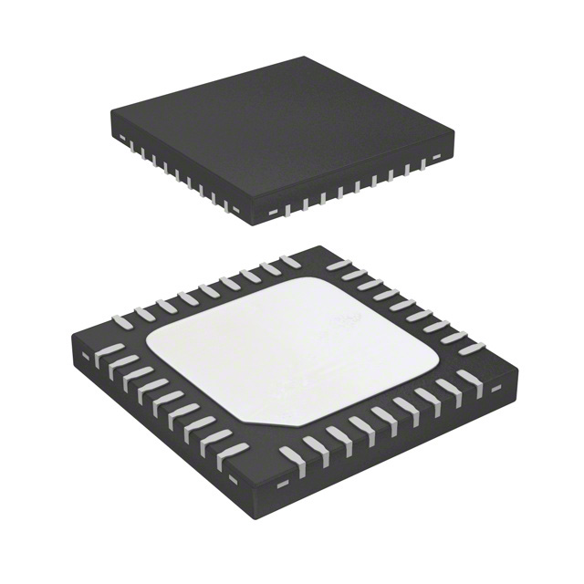
P-WQFN36-0606-0.50-002
Weight:0.14(g)
Features
・The TB67S213FTAG can operate a single bipolar stepping motor.
・PWM method current feedback control.
・Operational in Full, Half, and Quarter step resolutions.
・Uses low on-resistance MOSFETs for output stage.
・High voltage and large current. (For specification, please refer to the absolute maximum ratings
and operation ranges.)
・Error detection circuits (Thermal Shutdown(TSD), Over current shutdown(ISD), and Power-on reset(POR))
・The built-in VCC regulator allows the TB67S213FTAG to operate with a single VM power supply.
・Customizable PWM chopping frequency using the external components (resistance/condenser).
・Package:
TB67S213FTAG: P-WQFN36-0606-0.50-002
Note) Please be careful about thermal conditions during use.
1
2013-08-19
Ver.1.02
�TB67S213FTAG
Pin assignment
OUT_B+
OUT_B+
RS_B
RS_B
VM
NC
VCC
NC
NC
(Top View)
27 26 25 24 23 22 21 20 19
NC
28
18
GND
GND
29
17
OUT_B-
VREF_B
30
16
OUT_B-
VREF_A
31
15
GND
OSCM
32
14
NC
IN_A1
33
13
GND
IN_A2
34
12
OUT_A-
PHASE_A
35
11
OUT_A-
PHASE_B
36
10
GND
1
2
3
4
5
6
7
8
9
IN_B1
IN_B2
STANDBY
GND
NC
RS_A
RS_A
OUT_A+
OUT_A+
TB67S213FTAG
* Please make sure to short the corner pads and the backside exposed pad to the ground pattern of the board.
2
2013-08-19
Ver.1.02
�TB67S213FTAG
Block Diagram
PHASE_A
PHASE_B
IN_B1
IN_B2
STANDBY
VMR Detect
VCC Voltage
Regulator
Step Decoder
(Input Logic)
VCC
Chopper OSC
IN_A1
OSCM
IN_A2
OSC
Current Level Set
VREF
Torque Control
3bit D/A
(Angle Control)
CR-CLK
Converter
Current Control
VM
Current Feedback
Output Control
(Mixed Decay Control)
RS COMP
RS_A
RS_B
ISD/VRS
Output
(H-Bridge ×2)
VM
TSD
VMR
Detect
Detection Circuit
Stepping Motor
* Please note that in the block diagram, functional blocks or constants may be omitted or simplified for explanatory purposes.
* Please make sure that all GND pins are shorted to the board’s ground pattern with a single point. Also, make sure to take extra
care with pattern layout, due to heat generation.
Please take extra care while tracing the layout of the VM, GND and output patterns to avoid shortage across output, GND
or power supplies. If such shortage occurs, the TB67S213 may be permanently damaged.
The utmost care should also be taken for pattern designing and implementation of the TB67S213. If power-relevant pins such as
VM, RS, OUT, and GND (which is capable of running particularly large current) are wired incorrectly, an operation error may occur
or the TB67S213 may be destroyed. The logic input pins must also be wired correctly. Otherwise, the TB67S213 may be damaged
by a current larger than the specified current running through the IC.
3
2013-08-19
Ver.1.02
�TB67S213FTAG
Pin assignment / function
TB67S213FTAG (QFN36)
Pin No.1 - 36
Pin No.
Pin Name
Function
1
IN_B1
Bch step resolution control 1
2
IN_B2
Bch step resolution control 2
3
STANDBY
4
GND
5
NC
6
RS_A
Motor Ach current sense pin
7
RS_A
Motor Ach current sense pin
8
OUT_A+
Motor Ach (+) output pin
9
OUT_A+
Motor Ach (+) output pin
10
GND
11
OUT_A-
Motor Ach (-) output pin
12
OUT_A-
Motor Ach (-) output pin
13
GND
14
NC
Standby set pin
Ground pin
Non-connection pin
Ground pin
Ground pin
Non-connection pin
15
GND
16
OUT_B-
Ground pin
Motor Bch (-) output pin
17
OUT_B-
Motor Bch (-) output pin
18
GND
19
OUT_B+
Motor Bch (+) output pin
20
OUT_B+
Motor Bch (+) output pin
21
RS_B
Motor Bch current sense pin
22
RS_B
Motor Bch current sense pin
23
VM
VM power supply pin
24
NC
Non-connection pin
25
VCC
26
NC
Non-connection pin
27
NC
Non-connection pin
28
NC
Non-connection pin
29
GND
30
VREF_B
Motor Bch current threshold set pin
31
VREF_A
Motor Ach current threshold set pin
32
OSCM
Internal Oscillator frequency set pin
33
IN_A1
Ach step resolution control 1
34
IN_A2
Ach step resolution control 2
35
PHASE_A
Ach phase set pin
36
PHASE_B
Bch phase set pin
Ground pin
Internal VCC regulator monitor pin
Ground pin
・Please do not run patterns under NC pins.
・Please short the pins with the same pin names, while using the TB67S213.
4
2013-08-19
Ver.1.02
�TB67S213FTAG
Equivalent circuit
TB67S213FTAG(QFN36)
6,7
21,22
1kΩ
100kΩ
1,2,3,33,34,35,36
8,9
11,12
19,20
16,17
GND
GND
25
1kΩ
1kΩ
32
500Ω
30,31
GND
GND
The equivalent circuit diagrams may be simplified or some parts of them may be omitted for explanatory purposes.
Pin No
1
2
3
6,7
8,9
11,12
16,17
19,20
21,22
23
25
30
31
32
33
34
35
36
Pin name
IN_B1
IN_B2
STANDBY
RS_A
OUT_A+
OUT_A-
OUT_B-
OUT_B+
RS_B
VM
VCC
VREF_B
VREF_A
OSCM
IN_A1
IN_A2
PHASE_A
PHASE_B
5
2013-08-19
Ver.1.02
�TB67S213FTAG
Function explanation(Stepping motor control)
Note: The current is defined “+(plus)” when the motor current flows from OUT_X+ -> OUT_X-. Also, the current is defined
“-(minus)” when the motor current flows from OUT_X- -> OUT_X+.
Phase A
Phase B
Input
Output
Input
Output
PHASE_A
IN_A1
IN_A2
IOUT(A)
PHASE_B
IN_B1
IN_B2
IOUT(B)
H
H
H
100%
H
H
H
100%
L
H
H
-100%
H
H
H
100%
L
H
H
-100%
L
H
H
-100%
H
H
H
100%
L
H
H
-100%
IN_A1,IN_A2,IN_B1,IN_B2 is recommended to set to “Low” level during power-on sequence.
Phase A
Phase B
Input
Output
Input
Output
PHASE_A
IN_A1
IN_A2
IOUT(A)
PHASE_B
IN_B1
IN_B2
IOUT(B)
H
H
H
100%
H
H
H
100%
X
L
L
0%
H
H
H
100%
L
H
H
-100%
H
H
H
100%
L
H
H
-100%
X
L
L
0%
L
H
H
-100%
L
H
H
-100%
X
L
L
0%
L
H
H
-100%
H
H
H
100%
L
H
H
-100%
H
H
H
100%
X
L
L
0%
X: Don't care
6
2013-08-19
Ver.1.02
�TB67S213FTAG
Phase A
Phase B
Input
Output
Input
Output
PHASE_A
IN_A1
IN_A2
IOUT(A)
PHASE_B
IN_B1
IN_B2
IOUT(B)
H
H
L
71%
H
H
L
71%
H
L
H
38%
H
H
H
100%
X
L
L
0%
H
H
H
100%
L
L
H
-38%
H
H
H
100%
L
H
L
-71%
H
H
L
71%
L
H
H
-100%
H
L
H
38%
L
H
H
-100%
X
L
L
0%
L
H
H
-100%
L
L
H
-38%
L
H
L
-71%
L
H
L
-71%
L
L
H
-38%
L
H
H
-100%
X
L
L
0%
L
H
H
-100%
H
L
H
38%
L
H
H
-100%
H
H
L
71%
L
H
L
-71%
H
H
H
100%
L
L
H
-38%
H
H
H
100%
X
L
L
0%
H
H
H
100%
H
L
H
38%
X: Don't care
Other functions
Pin Name
PHASE_X
STANDBY
H
L
Notes
OUT_X+:H
OUT_X+:L
OUT_X-:L
OUT_X-:H
When set to “H”, the motor current is set to flow from
OUT_X+ -> OUT_X-.
Motor function ready
Standby mode
7
When the STANDBY pin is set to “Low”, the internal
OSC and motor output stage will be set to OFF
status; therefore the motor will not be operational.
2013-08-19
Ver.1.02
�TB67S213FTAG
Absolute maximum ratings (Ta = 25°C)
Characteristics
Motor power supply
Motor output voltage
Motor output current
VCC voltage
Symbol
VM
VOUT
IOUT
VCC
VIN(H)
VIN(L)
PD
TOPR
TSTR
Tj(max)
Digital input voltage
Power dissipation
Operating temperature
Storage temperature
Junction temperature
QFN36
Rating
40
40
2.5
6.0
6.0
-0.4
1.15
-20 to 85
-55 to 150
150
Unit
V
V
A
V
V
V
W
℃
℃
℃
Note
Note 1
Note 2
-
Note 1: While in use, please make sure that the motor current is controlled to be under 80 % of the
absolute maximum ratings. (In this case, about 2.0A (max) ).
Note 2: The value in the state where it is not mounted on the board
Ta: Ambient temperature.
Topr: Operating ambient temperature.
Tj: Operating junction temperature. The maximum junction temperature is limited by the thermal shutdown.
Note: Use the maximum junction temperature (Tj) at 120°C or less.
The maximum current cannot be used under certain thermal conditions.
Note: The absolute maximum ratings
The absolute maximum ratings are a specification that must not be exceeded, even for a moment.
Exceeding the ratings may cause device breakdown, damage or deterioration, and may result in injury by
explosion or combustion.
Operating Ranges (Ta=0 to 85℃)
Characteristics
Symbol
Min
Typ
Max
Unit
Motor power supply
VM
10
24
35
V
Motor output current
IOUT
-
1.0
2.0
A
VIN(H)
2.0
-
5.5
V
Logic ‘High’ level
VIN(L)
0
-
0.8
V
Logic ‘Low’ level
CLK input frequency
fCLK
-
-
100
kHz
PWM signal frequency range
fchop(range)
40
100
150
kHz
VREF reference voltage
Vref
GND
3.0
3.6
V
RS pin voltage
VRS
-
±1.0
±1.5
V
Logic input voltage
Note
Reference value: VM
Note 1:
The actual maximum current may be limited by the operating environment (operating conditions such as excitation
mode or operating duration, or by the surrounding temperature or board heat dissipation). Determine a realistic maximum current
by calculating the heat generated under the operating environment.
Note 2:
The maximum VRS voltage should not exceed the maximum rated voltage.
8
2013-08-19
Ver.1.02
�TB67S213FTAG
Electrical Specifications 1 (Ta=25℃, VM=24V, unless specified otherwise)
Characteristics
Logic input pin voltage
Logic input voltage hysterisis
Logic input pin current
Symbol
HIGH
LOW
HIGH
LOW
Power consumption
Motor
current
output
leakage Hi-side
Low-side
Bridge-to-Bridge current differential
Output current error relative to the
predetermined value
RS pin current
Drain-source ON-resistance
(The sum of high side & low side)
Test
Circuit
Test Condition
Min
Typ.
Max
Unit
VIN(H)
VIN(L)
VIN(HYS)
IIN(H)
IIN(L)
DC
DC
Logic input pins (Note)
Logic input pins (Note)
2
0
-
5.5
0.8
V
V
DC
DC
DC
100
-
33
-
300
50
1
mV
µA
µA
IM1
DC
-
2
3
mA
IM2
IM3
IOH
DC
DC
DC
Logic input pins (Note)
Logic input pins; VIN=3.3V
Logic input pins; VIN=0V
Output:OPEN,
Standby mode
Output:OPEN, ENABLE=L
Output:OPEN (Full step setting)
VRS=VM=40V,VOUT=0V
-
3.5
5
-
5
7
1
mA
mA
µA
IOL
ΔIOUT1
DC
DC
VRS=VM=VOUT=40V
Channel A and B differential
1
-5
0
5
µA
%
ΔIOUT2
DC
IOUT=1.0A
-5
0
5
%
IRS
DC
VRS=VM=24V
IOUT=2.0A,
Tj=25℃, (Hi-side+Low side
MOSFET)
0
-
10
µA
-
0.53
0.75
Ω
Ron(S)_PN
Note: VIN (L → H) is defined as the VIN voltage that causes the outputs (OUT_A+, OUT_A-, OUT_B+ and OUT_B-) to change
when a pin under test is gradually raised from 0 V. V IN (H → L) is defined as the V IN voltage that causes the outputs (OUT_A+,
OUT_A-, OUT_B+ and OUT_B-) to change when the pin is then gradually lowered.
The difference between V IN (L → H) and V IN (H → L) is defined as the input hysteresis.
Note: The internal circuits are designed to avoid miss-function or leakage current; when the logic signal is applied while the VM
voltage is not supplied. But for fail-safe, please control the power supply and ogic signal timing correctly.
9
2013-08-19
Ver.1.02
�TB67S213FTAG
Electrical Specifications 2 (Ta=25℃, VM=24V, unless specified otherwise)
Characteristics
Symbol
Test Circuit
Test Condition
Min
Typ.
Max
Unit
Vref input voltage
VREF
VM=24V,VCC=5V
GND
3.0
3.6
V
Vref input current
IREF
VREF=3.0V
-
0
1
μA
VCC voltage
VCC
ICC=5.0mA
4.75
5.0
5.25
V
VCC current
ICC
VCC=5.0V
-
2.5
5
mA
Vref gain
VREF(gain)
VREF=2.0V
1/5.2
1/5.0
1/4.8
-
TSD threshold (Note1)
TjTSD
-
140
150
170
℃
VM POR threshold
VMR
-
7.0
8.0
9.0
V
Over current threshold (Note2)
ISD
-
(3.1)
(4.0)
(5.0)
A
DC
Note 1:
Thermal shutdown (TSD) circuit
When the junction temperature of the device reaches the TSD threshold, the TSD circuit is triggered; the
internal reset circuit then turns off the output transistors. Once the TSD circuit is triggered, the device keeps the
output off until power-on reset (POR), is reasserted or set to Standby mode.
Note 2:
Over-current/voltage shutdown (ISD) circuit
When the output current or the RS pin voltage reaches the threshold, the ISD circuit is triggered; the internal
reset circuit then turns off the output transistors. Once the ISD circuit is triggered, the device keeps the output
off until power-on reset (POR), is reasserted or set to Standby mode.
For fail-safe, please insert a fuse to avoid secondary trouble.
Back-EMF
While a motor is rotating, there is a timing at which power is fed back to the power supply. At that timing, the motor current
recirculates back to the power supply due to the effect of the motor back-EMF.
If the power supply does not have enough sink capability, the power supply and output pins of the device might rise above the
rated voltages. The magnitude of the motor back-EMF varies with usage conditions and motor characteristics. It must be fully
verified that there is no risk that the TB67S213 or other components will be damaged or fail due to the motor back-EMF.
Cautions on Overcurrent Shutdown (ISD) and Thermal Shutdown (TSD)
•
The ISD and TSD circuits are only intended to provide temporary protection against irregular conditions such as an output
short-circuit; they do not necessarily guarantee the complete IC safety.
•
If the device is used beyond the specified operating ranges, these circuits may not operate properly: then the device may be
damaged due to an output short-circuit.
•
The ISD circuit is only intended to provide a temporary protection against an output short-circuit. If such a condition persists
for a long time, the device may be damaged due to overstress. Overcurrent conditions must be removed immediately by
external hardware.
IC Mounting
Do not insert devices incorrectly or in the wrong orientation. Otherwise, it may cause breakdown, damage and/or deterioration of
the device.
10
2013-08-19
Ver.1.02
�TB67S213FTAG
Electrical Specifications 2 (Ta = 25°C, VM = 24 V, 6.8 mH/5.7 Ω)
Symbol
Test
Circuit
Test Condition
Min
Typ.
Max
Unit
PHASE input frequency
fPHASE
AC
fOSC=1600kHz
-
-
150
kHz
Minimum PHASE High width
tPHASE(H)
AC
Minimum PHASE width:
PHASE=‘H’
50
-
-
ns
Minimum PHASE Low width
tPHASE(L)
AC
Minimum PHASE width:
PHASE=‘L’
50
-
-
ns
tr
AC
150
200
250
ns
Output stage
tf
AC
100
150
200
ns
Switching specifications
tpLH(CLK)
AC
PHASE to OUT
250
-
1200
ns
tpHL(CLK)
AC
PHASE to OUT
250
-
1200
ns
Analog noise rejection blank time
AtBLK
AC
250
400
550
ns
Internal oscillator frequency
fOSC
AC
COSC= 270 pF, ROSC =3.6 kΩ
1360
1600
1840
kHz
Motor chopping frequency
fchop
AC
Output active (IOUT =1.0 A),
fOSC = 1600 kHz
-
100
-
kHz
Characteristics
VM=24V,IOUT=1.0A
Analog tBLK
AC timing chart
fPHASE
tPHASE(L)
50%
50%
50%
tPHASE (H)
【PHASE】
tpHL(PHASE)
tpLH(PHASE)
90%
90%
50%
50%
【OUT】
10%
tf
tr
10%
Timing charts may be simplified for explanatory purpose.
11
2013-08-19
Ver.1.02
�TB67S213FTAG
Application Note
Motor control (Current feedback control)
The ‘Mixed Decay Timing’ is a fixed value of 37.5% of 1 fchop cycle.
fchop
OSC internal
waveform
IOUT
MDT
NF detect
Current
threshold
37.5% Mixed Decay Mode
Charge Mode → NF detect → Slow Mode → MixedDecay
Timing → Fast Mode → Charge Mode
6clk / 16clk
= 37.5% fchop
fchop 1cycle:16clk
Waveform of Mixed Decay Mode sequence (Motor current)
fchop
fchop
OSC internal
waveform
37.5% Mixed Decay Mode
Current
threshold
NF detect
NF detect
IOUT
MDT (Mixed Decay Timing): 37.5% fchop
Timing charts may be simplified for explanatory purposes.
Note: About Mixed Decay Timing
Mixed Decay Timing (MDT) is a unique value of the TB67S213 (fchop×37.5%), but when the motor output current
reaches NF threshold after MDT, the rest of fchop (※) becomes fast decay mode.
12
2013-08-19
Ver.1.02
�TB67S213FTAG
Mixed (Slow + Fast) Decay Mode current waveform
・When the next step’s current threshold is above the preious step
fchop
fchop
fchop
fchop
OSC internal
waveform
Current
threshold
NF
Slow
NF
Slow
Charge
NF
NF
Current
threshold
Fast
Charge
Slow
Fast
Charge
Slow
Fast
Fast
Charge
・When the next step’s current threshold is below the preious step
fchop
fchop
OSC internal
waveform
Current
threshold
NF
An instant ‘Charge Mode’ will enable the driver to
compare the motor current and the current threshold.
NF
Slow
Slow
Charge
fchop
fchop
NF
Charge
Fast
Fast
Charge
Current
threshold
Slow
NF
Fast
Charge
NF
Slow
Fast
Charge
Timing charts may be simplified for explanatory purposes.
13
2013-08-19
Ver.1.02
�TB67S213FTAG
Output Transistor Operation Mode
VM
VM
RRS
VM
RRS
RS
RRS
RS
RS
U1
U2
U1
U2
U1
U2
ON
ON
L1
L2
L1
ON
ON
GND
L2
L1
ON
L2
ON
GND
GND
Charge
Slow decay
Fast decay
Some of the functional blocks, circuits, or constants omitted or simplified for explanatory purpose.
Output Transistor Operational Function
Mode
U1
L1
U2
L2
Charge
ON
OFF
OFF
ON
Slow decay
OFF
ON
OFF
ON
Fast decay
OFF
ON
ON
OFF
Note: The parameters shown in the table above are examples when the current flows in the directions shown in the figures above.
For the current flowing in the reverse direction, the parameters change as shown in the table below.
Mode
U1
L1
U2
L2
Charge
OFF
ON
ON
OFF
Slow decay
OFF
ON
OFF
ON
Fast decay
ON
OFF
OFF
ON
14
2013-08-19
Ver.1.02
�TB67S213FTAG
Calculation of the Predefined Output Current
For PWM constant-current control, the TB67S213FTAG uses a clock generated by the CR oscillator.
The peak output current can be set via the current-sensing resistor (RRS) and the reference voltage
(Vref), as follows:
IOUT = Vref/5 ÷ RRS (Ω)
where, 1/5 is the Vref decay rate, Vref (GAIN). For the value of Vref (GAIN), see the Electrical
Characteristics table.For example, when Vref = 3 V, to set the current feedback threshold (Iout)=1.8A,
RS resistance is calculated as:
RRS = (Vref /5) ÷ IOUT = (3/5) ÷ 1.8 = 0.33Ω. (≥ 1.1 W)
Calculation of the OSCM oscillation frequency (chopper reference frequency)
An approximation of the OSCM oscillation frequency (fOSCM) and chopper frequency (fchop)
can be calculated by the following expressions.
fOSCM=1/[0.56x{Cx(R1+500)}]
………C,R1: External components for OSCM (C=270pF , R=3.6kΩ => 1.6MHz)
fchop = fOSCM / 16
IC Power Consumption
The
1)
2)
The
power consumed by the TB67S213FTAG is approximately the sum of the following:
the power consumed by the output transistors
the power consumed by the digital logic and pre-drivers.
power consumed by the output transistors is calculated, using the RON (D-S) value of 0.6Ω(typ).
An approximation of the peak power consumption for H-SW can be calculated by the following expressions.
P (out) = H-SW(ch) × Iout (A) × Iout (A) × Ron (Ω)
(1)
In full step operation (for example, 1.0A), the average power consumption in the output stage is
calculated as follows:
Ron = 0.6Ω , Iout = 1.0 A, VM = 24 V
P (out) = 2 (ch) × 1.0 (A)^2 × 0.6(Ω)
= 1.2 (W)
(2)
The power consumption in the IM domain is calculated as:
P (IM) = 24 (V) × 0.005 (A)
= 0.12 (W)
(3)
(IM3) = 5.0 mA (typ.), VM=24V
All over, the total peak power consumption of TB67S213FTAG is:
P = P (out) + P (IM) = 1.32 (W)
Board design should be fully verified, taking thermal dissipation into consideration.
15
2013-08-19
Ver.1.02
�TB67S213FTAG
Step resolution timing charts (PHASE-IN)
[Full step resolution]
100%
IOUT(A)
0%
-100%
100%
0%
-100%
PHASE_A
IN_A1
IN_A2
PHASE_B
IN_B1
IN_B2
H
L
H
L
H
L
H
L
H
L
H
L
Timing charts may be simplified for explanatory purposes.
16
2013-08-19
Ver.1.02
�TB67S213FTAG
[Half step resolution]
100%
IOUT(A)
0%
-100%
100%
IOUT(B)
0%
-100%
PHASE_A
IN_A1
IN_A2
PHASE_B
IN_B1
IN_B2
H
L
H
L
H
L
H
L
H
L
H
L
Timing charts may be simplified for explanatory purposes.
17
2013-08-19
Ver.1.02
�TB67S213FTAG
[Quarter step resolution]
IOUT_A
100%
71%
38%
0%
-38%
-71%
-100%
IOUT_B
100%
71%
38%
0%
-38%
-71%
-100%
PHASE_A
IN_A1
IN_A2
H
L
H
L
H
L
PHASE_B
IN_B1
IN_B2
H
L
H
L
H
L
Timing charts may be simplified for explanatory purposes.
18
2013-08-19
Ver.1.02
�TB67S213FTAG
Example Application Circuits
The values shown in the following figure are typical values. For input conditions, see the Operating Ranges.
RS_B
RS_B
VM
VCC
0.22Ω
OUT_B+
0.1µF
100µF
OUT_B+
24V
0.1µF
GND
0.1µF
GND
OUT_B-
GND
VREF_B
OUT_BGND
M
VREF_A
3.6kΩ
GND
OSCM
270pF
GND
PHASE_A
OUT_A+
OUT_A+
0.22Ω
RS_A
RS_A
PHASE_B
IN_B1
0V
5V
3.3V
OUT_A-
IN_A2
GND
0V
5V
3.3V
STANDBY
0V
5V
3.3V
OUT_AIN_A1
IN_B2
0V
5V
3.3V
5V
5V
5V
3.3V
3.3V
3.3V
0V
0V
0V
Note: Bypass capacitors should be added as necessary. It is recommended to use a single ground plane for the entire
board whenever possible.
The above application circuit example is presented only as a guide and should be fully evaluated prior to production.
Also, no intellectual property right is ceded in any way whatsoever in regard to its use.
19
2013-08-19
Ver.1.02
�TB67S213FTAG
Package Dimensions
P-WQFN36-0606-0.50-002
Unit:mm
20
2013-08-19
Ver.1.02
�TB67S213FTAG
Notes on Contents
Block Diagrams
Some of the functional blocks, circuits, or constants in the block diagram may be omitted or simplified for explanatory purposes.
Equivalent Circuits
The equivalent circuit diagrams may be simplified or some parts of them may be omitted for explanatory purposes.
Timing Charts
Timing charts may be simplified for explanatory purposes.
Application Circuits
The application circuits shown in this document are provided for reference purposes only. Thorough evaluation is required at the
mass production design stage. Toshiba does not grant any license to any industrial property rights by providing these examples of
application circuits.
Test Circuits
Components in the test circuits are used only to obtain and confirm the device characteristics. These components and circuits are
not guaranteed to prevent malfunction or failure from occurring in the application equipment.
IC Usage Considerations
Notes on handling of ICs
The absolute maximum ratings of a semiconductor device are a set of ratings that must not be exceeded, even for a moment. Do
not exceed any of these ratings.Exceeding the rating(s) may cause device breakdown, damage or deterioration, and may result in
injury by explosion or combustion.
Use an appropriate power supply fuse to ensure that a large current does not continuously flow in the case of over-current and/or
IC failure. The IC will fully break down when used under conditions that exceed its absolute maximum ratings, when the wiring is
routed improperly or when an abnormal pulse noise occurs from the wiring or load, causing a large current to continuously flow and
the breakdown can lead to smoke or ignition. To minimize the effects of the flow of a large current in the case of breakdown,
appropriate settings, such as fuse capacity, fusing time and insertion circuit location, are required.
If your design includes an inductive load such as a motor coil, incorporate a protection circuit into the design to prevent device
malfunction or breakdown caused by the current resulting from the inrush current at power ON or the negative current resulting
from the back electromotive force at power OFF. IC breakdown may cause injury, smoke or ignition. Use a stable power supply
with ICs with built-in protection functions. If the power supply is unstable, the protection function may not operate, causing IC
breakdown. IC breakdown may cause injury, smoke or ignition.
Do not insert devices in the wrong orientation or incorrectly. Make sure that the positive and negative terminals of power supplies
are connected properly. Otherwise, the current or power consumption may exceed the absolute maximum rating, and exceeding the
rating(s) may cause device breakdown, damage or deterioration, and may result in injury by explosion or combustion. In addition, do
not use any device that has been inserted incorrectly.
Please take extra care when selecting external components (such as power amps and regulators) or external devices (for
instance, speakers). When large amounts of leak current occurs from capacitors, the DC output level may increase.
If the output is connected to devices such as speakers with low resist voltage, overcurrent or IC failure may cause
smoke or ignition. (The over-current may cause smoke or ignition from the IC itself.) In particular, please pay
attention when using a Bridge Tied Load (BTL) connection-type IC that inputs output DC voltage to a speaker
directly.
21
2013-08-19
Ver.1.02
�TB67S213FTAG
Points to remember on handling of ICs
Over current detection circuit
Over current detection circuits (referred to as current limiter circuits) do not necessarily protect ICs under all
circumstances. If the Over current detection circuits operate against the over current, clear the over current
status immediately.
Depending on the method of use and usage conditions, such as exceeding absolute maximum ratings can cause the
over current protection circuit to not operate properly or IC breakdown before operation. In addition, depending on
the method of use and usage conditions, if over current continues to flow for a long time after operation, the IC
may generate heat resulting in breakdown.
Thermal Shutdown Circuit
Thermal shutdown circuits do not necessarily protect ICs under all circumstances. If the thermal shutdown circuits
operate against the over temperature, clear the heat generation status immediately.
Depending on the method of use and usage conditions, such as exceeding absolute maximum ratings can cause the
thermal shutdown circuit to not operate properly or IC breakdown before operation.
Heat Radiation Design
In using an IC with large current flow such as power amp, regulator or driver, please design the device so that heat
is appropriately radiated, not to exceed the specified junction temperature (TJ) at any time and condition. These
ICs generate heat even during normal use. An inadequate IC heat radiation design can lead to decrease in IC life,
deterioration of IC characteristics or IC breakdown. In addition, please design the device taking into considerate the
effect of IC heat radiation with peripheral components.
Back-EMF
When a motor rotates in the reverse direction, stops or slows down abruptly, a current flow back to the motor’s power supply due
to the effect of back-EMF. If the current sink capability of the power supply is small, the device’s motor power supply and output
pins might be exposed to conditions beyond maximum ratings. To avoid this problem, take the effect of back-EMF into
consideration in system design.
22
2013-08-19
Ver.1.02
�TB67S213FTAG
RESTRICTIONS ON PRODUCT USE
• Toshiba Corporation, and its subsidiaries and affiliates (collectively "TOSHIBA"), reserve the right to make changes to the information in
this document, and related hardware, software and systems (collectively "Product") without notice.
• This document and any information herein may not be reproduced without prior written permission from TOSHIBA. Even with TOSHIBA's
written permission, reproduction is permissible only if reproduction is without alteration/omission.
• Though TOSHIBA works continually to improve Product's quality and reliability, Product can malfunction or fail. Customers are
responsible for complying with safety standards and for providing adequate designs and safeguards for their hardware, software and
systems which minimize risk and avoid situations in which a malfunction or failure of Product could cause loss of human life, bodily injury
or damage to property, including data loss or corruption. Before customers use the Product, create designs including the Product, or
incorporate the Product into their own applications, customers must also refer to and comply with (a) the latest versions of all relevant
TOSHIBA information, including without limitation, this document, the specifications, the data sheets and application notes for Product
and the precautions and conditions set forth in the "TOSHIBA Semiconductor Reliability Handbook" and (b) the instructions for the
application with which the Product will be used with or for. Customers are solely responsible for all aspects of their own product design or
applications, including but not limited to (a) determining the appropriateness of the use of this Product in such design or applications; (b)
evaluating and determining the applicability of any information contained in this document, or in charts, diagrams, programs, algorithms,
sample application circuits, or any other referenced documents; and (c) validating all operating parameters for such designs and
applications. TOSHIBA ASSUMES NO LIABILITY FOR CUSTOMERS' PRODUCT DESIGN OR APPLICATIONS.
• PRODUCT IS NEITHER INTENDED NOR WARRANTED FOR USE IN EQUIPMENTS OR SYSTEMS THAT REQUIRE
EXTRAORDINARILY HIGH LEVELS OF QUALITY AND/OR RELIABILITY, AND/OR A MALFUNCTION OR FAILURE OF WHICH MAY
CAUSE LOSS OF HUMAN LIFE, BODILY INJURY, SERIOUS PROPERTY DAMAGE AND/OR SERIOUS PUBLIC IMPACT
("UNINTENDED USE"). Except for specific applications as expressly stated in this document, Unintended Use includes, without
limitation, equipment used in nuclear facilities, equipment used in the aerospace industry, medical equipment, equipment used for
automobiles, trains, ships and other transportation, traffic signaling equipment, equipment used to control combustions or explosions,
safety devices, elevators and escalators, devices related to electric power, and equipment used in finance-related fields. IF YOU USE
PRODUCT FOR UNINTENDED USE, TOSHIBA ASSUMES NO LIABILITY FOR PRODUCT. For details, please contact your TOSHIBA
sales representative.
• Do not disassemble, analyze, reverse-engineer, alter, modify, translate or copy Product, whether in whole or in part.
• Product shall not be used for or incorporated into any products or systems whose manufacture, use, or sale is prohibited under any
applicable laws or regulations.
• The information contained herein is presented only as guidance for Product use. No responsibility is assumed by TOSHIBA for any
infringement of patents or any other intellectual property rights of third parties that may result from the use of Product. No license to any
intellectual property right is granted by this document, whether express or implied, by estoppel or otherwise.
• ABSENT A WRITTEN SIGNED AGREEMENT, EXCEPT AS PROVIDED IN THE RELEVANT TERMS AND CONDITIONS OF SALE
FOR PRODUCT, AND TO THE MAXIMUM EXTENT ALLOWABLE BY LAW, TOSHIBA (1) ASSUMES NO LIABILITY WHATSOEVER,
INCLUDING WITHOUT LIMITATION, INDIRECT, CONSEQUENTIAL, SPECIAL, OR INCIDENTAL DAMAGES OR LOSS, INCLUDING
WITHOUT LIMITATION, LOSS OF PROFITS, LOSS OF OPPORTUNITIES, BUSINESS INTERRUPTION AND LOSS OF DATA, AND
(2) DISCLAIMS ANY AND ALL EXPRESS OR IMPLIED WARRANTIES AND CONDITIONS RELATED TO SALE, USE OF PRODUCT,
OR INFORMATION, INCLUDING WARRANTIES OR CONDITIONS OF MERCHANTABILITY, FITNESS FOR A PARTICULAR
PURPOSE, ACCURACY OF INFORMATION, OR NONINFRINGEMENT.
• Do not use or otherwise make available Product or related software or technology for any military purposes, including without limitation,
for the design, development, use, stockpiling or manufacturing of nuclear, chemical, or biological weapons or missile technology
products (mass destruction weapons). Product and related software and technology may be controlled under the applicable export laws
and regulations including, without limitation, the Japanese Foreign Exchange and Foreign Trade Law and the U.S. Export Administration
Regulations. Export and re-export of Product or related software or technology are strictly prohibited except in compliance with all
applicable export laws and regulations.
• Please contact your TOSHIBA sales representative for details as to environmental matters such as the RoHS compatibility of Product.
Please use Product in compliance with all applicable laws and regulations that regulate the inclusion or use of controlled substances,
including without limitation, the EU RoHS Directive. TOSHIBA ASSUMES NO LIABILITY FOR DAMAGES OR LOSSES OCCURRING
AS A RESULT OF NONCOMPLIANCE WITH APPLICABLE LAWS AND REGULATIONS.
23
2013-08-19
Ver.1.02
�