TB9101FNG
TOSHIBA Bi-CMOS Linear Integrated Circuit Silicon Monolithic
TB9101FNG
2ch H-Bridge driver for DC Brushed Motor
TB9101FNG is a 2ch H-bridge driver which is designed
specifically for Automotive. This IC has built-in for directly
driving small DC Brushed motor.
Forward/Reverse/Stop/Brake can be set by Input
signal (DI1A,DI1B,DI2A,DI2B). These Inputs are TTL,
thus, TB9101FNG can be controlled by external MCU,
directory. Standby mode, Miscellaneous Abnormal
Detection are built-in.
TB9101FNG is for wide application such as for Automotive
Air-condition system (Dumper control), Door Mirror control.
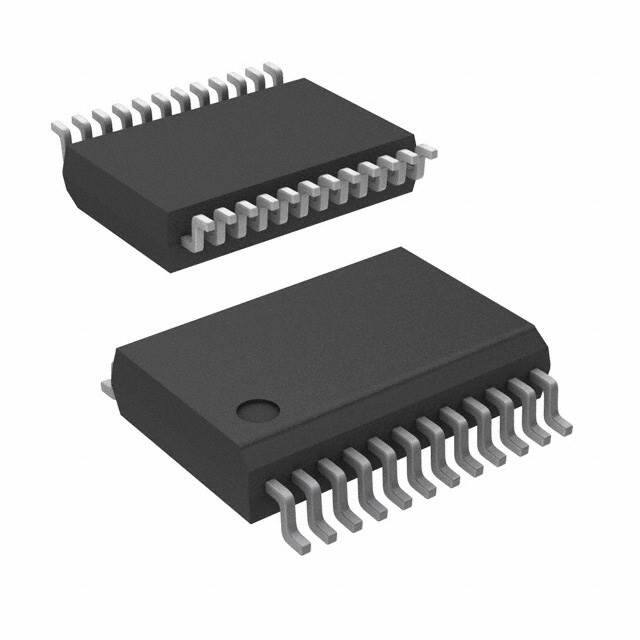
SSOP24-P-300-0.65A
Weight: 0.14 g (typ.)
Feature
··Motor Driver
: 2ch H-Bridge with Driver (Directry drive external Motor)
RON: RHON(Pch)=0.6Ω(typ.), RLON(Nch)=0.6Ω(typ.)
··Standby mode
: 0mA(typ.)
··Operating Voltage range : 7 to 18V (Absolute Maximum Rating 40V)
··Operating Temperature range
: -40°C to 125°C
··Miscellaneous Abnormal Detection
:
··Package
Motor Over Current (with Output monitor signal)
VCC Over Voltage
VCC Low Voltage
IC internal Over Temperature
: SSOP24-P-300-0.65A
··AEC-Q100 Qualified
··The product(s) is/are compatible with RoHS regulations (2011 / 65 / EU) as indicated,
if any, on the packaging label ("[[G]]/RoHS COMPATIBLE", "[[G]]/RoHS [[Chemical symbol(s) of
controlled substance(s)]]", "RoHS COMPATIBLE" or "RoHS COMPATIBLE,
[[Chemical symbol(s) of controlled substance(s)]]>MCV").
©2014–2019
Toshiba Electronic Devices & Storage Corporation
1
2019-2-25
�TB9101FNG
INTERNAL BLOCK DIAGRAM AND PIN LAYOUT
NC
23
DI2A
24
DI2B
22
L・G2
21
DG2
20
NC
19
NC
18
M+2
17
P・G2
16
NC
15
M-2
14
Vcc2
13
Over Current
Diagnostic
Signal for ISD
Dead Time
1μs
Control LOGIC
Over
Temp.
5V Regulator
Over Voltage
Low Voltage
5V Reglator
Over Voltage
Low Voltage
Over Current
Over
Temp.
Over Current
Dead Time
1μs
Control LOGIC
Diagnostic
Signal for ISD
Over Current
1
DI1A
*1:
2
NC
3
DI1B
4
L・G1
5
DG1
6
NC
7
NC
8
M+1
9
P・G1
10
NC
11
M-1
12
Vcc1
VCC1
Some of the functional blocks, circuit, or constants in the block diagram may be omitted or
Simplified for explanatory purpose.
*2: Install the product correctly. Otherwise, it may result in break down, damage and/or
deterioration to the product or equipment.
2
2019-2-25
�TB9101FNG
·PIN CONNECTION
PIN No.
PIN NAME
NOTES
CH1 CH2 CH1
CH2
1
3
24
22
DI1A
DI1B
DI2A
DI2B
Input for Motor control.(refer to “Motor Operation1” in next page)
4
21
L・G1
L・G2
GND for 5V Circuit.
5
20
DG1
DG2
8
17
M +1
M +2
Over Current Detection Monitor signal. The Output is Open Drain
type. When Over Current is detected on each Motor, DG1/DG2
output “L”. External Pull Up to 5V is required.
Output for Motor 1,2 drivring. Build-in Over Current detection.
9
16
P・G1
P・G2
GND for Motor driving.
11
14
M -1
M -2
Output for Motor 1,2 drivring., Build-in Over Current detection
VCC1
VCC2
12V Power Supply(typ.). Build-in Over/Low Voltage Detecion
12
13
2,6,7,10,
15,18,19,
23
NC
no connecton. keep open on PCB
Internal protection circuit
Terminal
No.
1
2
3
4
5
6
7
8
9
10
11
12
13
14
15
16
17
18
19
20
21
22
23
24
Name
Internal Protection circuit
DI1A
NC
DI1B
L・G1
DG1
NC
NC
M+1
P・G1
NC
M-1
VCC1
VCC2
M-2
NC
P・G2
M+2
NC
NC
DG2
L・G2
DI2B
NC
DI2A
A Type(VCC1/ L・G1)
-
A Type(VCC1/ L・G1)
B Type(VCC1)
A Type(VCC1/ L・G1)
-
-
-
B Type(VCC1)
-
-
C Type(VCC2/ L・G1)
C Type(VCC1/ L・G2)
-
-
B Type(VCC2)
-
-
-
A Type(VCC2/ L・G2)
B Type(VCC2)
A Type(VCC2/ L・G2)
-
A Type(VCC2/ L・G2)
3
AType
VCC1
or VCC2
BType
VCC1
or VCC2
CType
VCC1
or VCC2
2019-2-25
�TB9101FNG
FUNCTIONAL DESCRIPTION
(1) Motor control
TB9101FNG build-in 2 H-Bridge. These 2 H-Bridge is controlled by Input DI1A/DI1B
DI2A/DI2B, independently. The operation modes are as follows.
·Motor Operation 1
Input
DI1A / DI2A DI1B / DI2B
H
H
H
L
L
H
L
L
Output
M +1 / M+2
M -1 / M-2
L
L
H
L
L
H
OFF (Hi-Z)
Operation Mode
BRAKE
FORWARD Rotation(CW)
REVERSE Rotation(CCW)
STANDBY
CAUTION: When Motor operation is stopped, it is prefer to go to BRAKE mode, first.
Then after reducing Motor rotation speed, goes to STANDBY mode. It can
be reducing Motor Back Electromotive Force.
·H-Bridge Circuit in Standby mode and BRAKE mode
Brake mode
Standby mode
VCC1/2
OFF
VCC1/2
OFF
OFF
M
OFF
OFF
M
OFF
ON
ON
●Standby mode: DI1A/DI1B = ”L”, DI2A/DI2B = ”L”
·5V Regulator OFF
·Motor Drive Output (M+1/M-1, M+2/M-2) OFF(Hi-Z)
·Abnormal Detection Circuit OFF (VCC Over Voltage, Over Current, Over Temp.
VCC Low Voltage)
4
2019-2-25
�TB9101FNG
·DEAD TIME Generation
TB9101FNG generate “DEAD TIME” on Motor drive output signal (M+1,M+2,M-1,M-2)
which is Hi-Z status during 1μs(typ.). at rising Edge of each Input (DI1A,DI1B,DI2A,DI2B) .
This is to protect power short by simultaneous ON of Hi-side and Lo-side MOSFET which
consist of the same Half Bridge.
H
L
DI1A (DI2A)
L
H
DI1B (DI2B)
H
L
M+1(M+2)
Hi-Z
L
L
1μs
H
M-1(M-2)
L
1μs
BRAKE
mode
Hi-Z
Standby
mode
VCC1/2
DI1B (DI2B)
DI1A (DI2A)
M+1
(M+2)
M
5
M-1
(M-2)
2019-2-25
�TB9101FNG
·Miscellaneous Abnormal Detection
TB9101FNG has Miscellaneous Abnormal Detection, such as Over Voltage (VSD) for VCC1,VCC2
Motor Over Current (ISD), CHIP inner Over Temperature(TSD), Low Voltage for VCC1,VCC2. These
Detection are set for each H-Bridge independently.
(VSD: detection 30V(typ.))
(1). Over Voltage Detection for VCC1,VCC2
TB9101FNG has Over Voltage Detection for VCC1 and VCC2, independently. When each
voltage is over 30V(typ.), the driver of that H-Bridge Output is turned OFF(Hi-Z). When
the voltage drop to lower than 27V(typ.), the driver return to normal operation which is
controlled by each Input (DI1A,DI1B,DI2A,DI2B). The internal signal of Over Voltage
Detection has chattering protection circuit. If the voltage continues to exceed the Over Voltage
Detection value, though the state of the Over Voltage Detection is released by the above mentioned,
the Over Voltage Detection is enabled again, and each output of the motor driver is turned
OFF(Hi-Z) again.
30V
(typ.)
Detect Over
Voltage (VSD)
Ret. To
Normal operation
VCC1(VCC2)
VSD-3 V
(typ.)
CAUTION1:This Over Voltage Detection is not to clamp Battery Voltage for TB9101FNG
Thus, the system should keep lower operation voltage than the Maximum
rating Spec.
(2). Over Temperature Detection (TSD: detection typ.170°C)
TB9101FNG has Over Temperature Detection for each internal H-Bridge, independently.
When the Temp of H-Bridge is over 170°C.(typ.), that H-Bridge Output is turned OFF(Hi-Z).
After detecting TSD, when that H-Bridge Temp. drop to lower than TSD-10°C (typ.), the
driver return to normal operation which is controlled by each Input (DI1A,DI1B,DI2A,DI2B)
The internal signal of Over Temperature Detection has chattering protection circuit. If the
temperature continues to exceed the Over Temperature Detection value, though the state of the
Over Temperature Detection is released by the above-mentioned, the Over Temperature Detection
is enabled again, and each output of the motor driver is turned OFF(Hi-Z) again.
170℃
(typ.)
CHIP
TEMP
Detect Over
CHIP Temp.
(TSD)
Ret. To
Normal operation
TSD-10°C
TSD-10deg
(typ.)
(typ.)
CAUTION2: The Absolute maximum Temperature of TB9101FNG is 150°C(Max). This Over
Temperature Detection function does not intend to limit the CHIP temperature.
Thus, the above Absolute Maximum Temperature never is over to use
TB9101FNG. If any of these rating would be exceeded during operation, the
device electrical characteristics may be irreparably altered and the reliability
and lifetime of the device can no longer be guaranteed. Moreover, these
operations with exceeded ratings may cause break down, damage and/or
degradation to any other equipment. Applications using the device should
be designed such that each maximum rating will never be exceeded in any
operating conditions. Before using, creating and/or producing designs, refer
6
2019-2-25
�TB9101FNG
to and comply with the precautions and conditions set forth in this documents.
In addition, this IC has a built-in over-temperature detection function, but this function
does not reduce to 170 °C below the temperature of the IC.
Also for the function of the operation guarantee range, please use as an auxiliary.
This Over Temp. Detection is worded over the Max. Rating Temperature and
shipping test does not perform at the Max. Rating Temp.
(3). Over Current Detection (ISD: detection typ. 1.5A )
TB9101FNG has Over Current of Motor Detection for each H-Bridge independently. When Motor
Current is over ±1.5A(typ.), that H-Bridge Output is turned OFF(Hi-Z), and each Diagnostic
signal (DG1,DG2) is changed to “L”. This Diagnostic signal DG1 and DG2 are the Output of
Open-Drain typ. Thus, the status in normal operation is “Hi-Z” and external Pull up to 5V
power line is required. After detecting Over Current of each H-Bridge, that Output for Motor
drive are kept OFF(Hi-Z) and Diagnostic signal of each H-Bridge(DG1, DG2) is kept “L”, even
the Current return to normal level. This Over Current Detection condition can be reset by going
to Standby mode (DI1A=DI1B=L or DI2A=DI2B=L). The internal signal of Over Current Detection
and Release has a chattering protection circuit to prevent mulfunction. If the Motor Current is still
over after reset by Standby mode operation, TB9101FNG detect it after going to Motor operation
from Standby mode (change anyone of that H-bridge Input (DI1A/DI1B or DI2A/DI2B) to “H”), and
change Motor drive Output to Hi-Z and output ”L” from each DG1/DG2, again.
When VCC Low Voltage is detected (5v typ.) after Over Current detection, Over Current
detection status is reset by Power On Reset. Thus, in this case, even the Voltage return to
normal and mode return to normal operation, previous Over Current Detection status does not
be held. The internal signal of Over Current Detection has chattering protection circuit.
Over Current
Detection (1.5A typ.)
to Standby mode
(DI1A,DI1B=”L”)
Input DI1A,DI1B
for Motor operation
H-Bridge OFF (Hi-Z)
Driver Curret
DG1/DG2
Standby
(Hi-Z)
“L”
(Hi-Z)
CAUTION:Over Current Detection circuits is only intended to provide temporary
protection against irregular conditions such as an output short-circuit;
they do not necessarily guarantee the complete IC safety.
Therefore, output short-circuit(short to VCC or GND) the ground fault
Since the IC may be destroyed, the design of routing output line, VCC, and GND
lines sufficient attention Please.
7
2019-2-25
�TB9101FNG
(4) Low Voltage Detection for VCC1,VCC2 (detection typ. 5V)
TB9101FNG has Low Voltage Detection for VCC1 and VCC2, independently. When each
voltage drop to lower than 5V(typ.), Power On Reset is done and the Output of that H-Bridge
is turned OFF(Hi-Z). Also Over Current Detection and Over Temperature Detection are OFF.
When the voltage rise up to 5.5V (typ.), the driver return to normal operation which is
controlled by each Input (DI1A,DI1B,DI2A,DI2B).
Release signal and Low Voltage Detection is designed to prevent a malfunction and a built-in
chattering prevention circuit.
Power ON
Power ON Reset
Voltage (5V typ.)
VCC1
VCC2
Start Normal
Operation
(5.5V typ.)
Recover
Voltage
Low
Voltage
Normal
Operation
Normal
Operation
Start Normal
Operation
(5.5V typ.)
Power ON Reset
Voltage (5V typ.)
0V
Internal
RESET
Signal
Motor
Operation
OFF
(Hi-Z)
OFF
(Hi-Z)
Operation
8
Operation
2019-2-25
�TB9101FNG
·ELECTRICAL CHARACTERISTICS
(1) ABSOLUTE MAXIMUM RATING (Ta=25°C)
ITEM
Supply Voltage
Output Current
SYMBOL
PIN
VCC
IOUT
IOL
Input Voltage
VIN
Output Voltage
VOUT
Operating Temp.
Storage Temp.
Soldering
Temp./Time
Topr
Tstg
Tsol
Power Dissipation
PD
CONDITION
RATING
VCC1,VCC2
M+1, M-1,
M+2, M-2
DC Voltage
at Current Detection
-0.3 to +40
±1.5
-
±1.0
DG1,DG2
DI1A, DI1B
DI2A, DI2B
M+1, M-1,
M+2, M-2
DG1,DG2
-
-
-
-
+2.5
mA
-
-0.3 to +40
V
-
-0.3 to +40
V
-
-
-
Manual Soldering
-40 to +125
-55 to +150
260 (10s)
PCB
76.2×114.3×t1.6mm
1.32
Mono Layer, Cu:30%
CAUTION 1:The above current spec. value of “+” is Input from outside,”-“ is Output from
TB9101FNG.
CAUTION 2: Please do not exceed the absolute maximum rating, including the reverse voltage.
CAUTION 3:The absolute maximum ratings of a semiconductor device are a set of specified
parameter values, which must not be exceeded during operation, even for an
instant. If any of these rating would be exceeded during operation, the device
electrical characteristics may be irreparably altered and the reliability and
lifetime of the device can no longer be guaranteed. Moreover, these operations
with exceeded ratings may cause break down, damage and/or degradation to
any other equipment. Applications using the device should be designed such
that each maximum rating will never be exceeded in any operating conditions.
Before using, creating and/or producing designs, refer to and comply with the
precautions and conditions set forth in these documents.
SYMBOL
ITEM
°C
W
Thermal Resistance
CONDITION
RATING
160
UNIT
IC
PCB Mono Layer, size:76.2×114.3×t1.6mm,
95
Thermal Resistance
Rθj-a
Cu:30%, Cu thickness:35μm
PCB 4Layer, size:76.2×114.3×t1.6mm
60
Cu:30%, Cu thickness:35μm
PD (W)
(1) PD max -Ta(Reference Data)
1.32
V
A
-
Package (SSOP24-P-300-0.65A)
UNIT
°C/W
°C/W
°C/W
PCB size:76.2×114.3×1.6mm
Cu 30%,Mono Layer
PD = (150 – Ta)/Rθj-a
I C (Single)
0.78
IC(no PCB) at 25°C.
(150-25)/160 = 0.781 (W)
0.67
using PCB(Mono Layer) size:76.2×114.3×1.6mm
Cu 30% at 25°C.
(150-25)/95 = 1.32(W)
0.53
0.24
0.16
0
25
85
125
150
Ta (°C)
9
2019-2-25
�TB9101FNG
·ELECTRICAL CHARACTERISTICS (cont.)
(2) IC CHARACTERISTICS
The following are under condition VCC1,VCC2 = 7 to 18V, Ta=-40 to 125°C. unless otherwise follows
ITEM
Current
Consumption
(No Load)
SYMBOL
Standby Current
Istby
Input Voltage
Input Current
Output Voltage
“L”
Input Current
“H”
ICC
VIL
VIH
PIN
Condition
CH1 or 2 CW or CCW
VCC1+VCC2 CH1+2 CW or CCW
CH1+2 BRAKE
VCC1, VCC2 DI1A,DI2A,DI1B,
DI2B=L
DI1A, DI1B,
DI2A, DI2B
MIN
TYP.
MAX
UNIT
-
-
7
mA
-
0
10
-
-
-
0.8
-
2.0
-
-
μA
V
DI1A, DI1B,
DI2A, DI2B
VIN=0.4V
-
5
10
VIN=5V
10
50
100
VOL
DG1, DG2
IOL=2.5mA
-
-
0.4
V
IIH
DG1, DG2
V(DG1,DG2)=18V
-
-
10
μA
IIL
IIH
10
2019-2-25
μA
�TB9101FNG
·ELECTRICAL CHARACTERISTICS (cont.)
(3) MOTOR DRIVER
The following are under condition VCC1,VCC2 = 7 to 18V, Ta=-40 to 125°C. unless otherwise follows
ITEM
H-side Output
ON Resistance
L-side Output
ON Resistance
Output OFF
Leak Current
SYMBOL
RHON
RLON
PIN
Condition
MIN
TYP.
MAX
IOUT=-0.5A,Ta=+25°C
-
0.60
1.2
IOUT=-0.5A,Ta=125°C
-
1.0
-
IOUT=-0.5A,Ta=-40°C
0.22
0.44
-
-
0.60
1.2
-
1.0
-
0.23
0.46
-
-10
-
-
10
IOUT=+0.5A,Ta=+25°C
M+1, M-1 IOUT=+0.5A,Ta=125°C
M+2, M-2 IOUT=+0.5A,Ta=-40°C
Output OFF VOUT=0V
ILO
UNIT
Output OFF
VOUT=VCC1, 2
tpHL
Rload=100Ω
3
10
Output Delay Time
tpLH
Rload=100Ω
3
10
CAUTION:When Motor is rotated, it makes Electromotive Force. The Electrical Specification
must be kept, even with this Electromotive Force.
DIA、DIB
M+、M-
90%
Hi-z
10%
tpHL/tpLH
3μs(typ.)
DeadTime
=1μs(typ.)
11
2019-2-25
Ω
μA
μs
�TB9101FNG
·ELECTRICAL CHARACTERISTICS (cont.)
(4) ABNORMAL DETECTION
The following are under condition VCC1,VCC2 = 7 to 18V, Ta=-40 to 125°C. Unless otherwise follows
ITEM
SYMBOL
Over Voltage
VSD
Detection ON
Over Voltage
VSD(hys)
Detection OFF
Over Temperature
TSD
Detection ON
Over Temperature
Detection OFF
Over Current
Detection
Low Voltage
Detection ON
Low Voltage
Detection OFF
TSD(hys)
ISD
VRSTH
VRSTL
PIN
Condition
VCC1
VCC2
-
-
*1
M+1, M-1
M+2, M-2
VCC1,
VCC2
VCC1,
VCC2
-
MIN
TYP.
MAX
27
30
33
-
VSD-3
-
150
170
190
TSD-5
UNIT
TSD-10 TSD-20
±1
±1.5
±2.5
-
5.0
-
4.5
5.5
6.0
Note *1: Impossible to test in mass production
12
2019-2-25
V
°C
A
V
�TB9101FNG
REFERENCE APPLICATION CIRCUIT DIAGRAM
VCC
VDD
+
Po1
Po2
Po3
System
Po4
Po5
Po6
DI1A
DI1B
DG1
DI2A
DI2B
DG2
VCC1 VCC2
M+1
M
M-1
TB9101FNG
M+2
M
M-2
L・G1 L・G2 P・G1 P・G2
CAUTION1: The capacitor connected to VCC, and connect to absorb, such as voltage fluctuations
due to motor load variation and noise from the outside.
Therefore, please be connected as close to the IC as much as possible.
CAUTION2: Install the product correctly. Otherwise, it may result in break down, damage and/or
deterioration to the product or equipment.
CAUTION3: The application circuits shown in this document are provided for reference purposes
only. Especially, a thorough evaluation is required on the phase of mass production
design.
Toshiba dose not grant the use of any industrial property rights with these examples
of application circuits.
CAUTION4: Short Circuit between each Output signal, Output Signal and Power line (Battery,
Regurator Output, GND) may make the cause of IC distruction or Damage.
CAUTION5: Overvoltage detection function does not clamp the power potential.
VCC supply must be protected externally so as not to absolute maximum ratings
over.
13
2019-2-25
�TB9101FNG
PACKAGE
SSOP24-P-300-0.65A
Unit: mm
Detailed diagram of tip of terminal
Weight: 0.14 g (typ.)
14
2019-2-25
�TB9101FNG
【CAUTION 】
·Some of the functional blocks, circuits, or constants in the block diagram may be omitted or
Simplified for explanatory purpose.
·The equivalent circuit diagrams may be simplified or some parts of them may be omitted for
explanatory purpose.
·Timing charts may be simplified for explanatory purpose.
·The absolute maximum ratings of a semiconductor device are a set of specified parameter
values, which must not be exceeded during operation, even for an instant. If any of these
rating would be exceeded during operation, the device electrical characteristics may be
irreparably altered and the reliability and lifetime of the device can no longer be guaranteed.
Moreover, these operations with exceeded ratings may cause break down, damage and/or
degradation to any other equipment. Applications using the device should be designed
such that each maximum rating will never be exceeded in any operating conditions. Before
using, creating and/or producing designs, refer to and comply with the precautions and
conditions set forth in this documents.
·Ensure that the IC is mounted correctly. Failing to do so may result in the IC or target
equipment being damage
15
2019-2-25
�TB9101FNG
RESTRICTIONS ON PRODUCT USE
Toshiba Corporation and its subsidiaries and affiliates are collectively referred to as “TOSHIBA”.
Hardware, software and systems described in this document are collectively referred to as “Product”.
• TOSHIBA reserves the right to make changes to the information in this document and related Product without notice.
• This document and any information herein may not be reproduced without prior written permission from TOSHIBA. Even with
TOSHIBA's written permission, reproduction is permissible only if reproduction is without alteration/omission.
• Though TOSHIBA works continually to improve Product's quality and reliability, Product can malfunction or fail. Customers are
responsible for complying with safety standards and for providing adequate designs and safeguards for their hardware, software and
systems which minimize risk and avoid situations in which a malfunction or failure of Product could cause loss of human life, bodily
injury or damage to property, including data loss or corruption. Before customers use the Product, create designs including the Product,
or incorporate the Product into their own applications, customers must also refer to and comply with (a) the latest versions of all
relevant TOSHIBA information, including without limitation, this document, the specifications, the data sheets and application notes for
Product and the precautions and conditions set forth in the "TOSHIBA Semiconductor Reliability Handbook" and (b) the instructions for
the application with which the Product will be used with or for. Customers are solely responsible for all aspects of their own product
design or applications, including but not limited to (a) determining the appropriateness of the use of this Product in such design or
applications; (b) evaluating and determining the applicability of any information contained in this document, or in charts, diagrams,
programs, algorithms, sample application circuits, or any other referenced documents; and (c) validating all operating parameters for
such designs and applications. TOSHIBA ASSUMES NO LIABILITY FOR CUSTOMERS' PRODUCT DESIGN OR APPLICATIONS.
• PRODUCT IS NEITHER INTENDED NOR WARRANTED FOR USE IN EQUIPMENTS OR SYSTEMS THAT REQUIRE
EXTRAORDINARILY HIGH LEVELS OF QUALITY AND/OR RELIABILITY, AND/OR A MALFUNCTION OR FAILURE OF WHICH
MAY CAUSE LOSS OF HUMAN LIFE, BODILY INJURY, SERIOUS PROPERTY DAMAGE AND/OR SERIOUS PUBLIC IMPACT
("UNINTENDED USE"). Except for specific applications as expressly stated in this document, Unintended Use includes, without
limitation, equipment used in nuclear facilities, equipment used in the aerospace industry, and lifesaving and/or life supporting medical
equipment. IF YOU USE PRODUCT FOR UNINTENDED USE, TOSHIBA ASSUMES NO LIABILITY FOR PRODUCT. For details,
please contact your TOSHIBA sales representative or contact us via our website.
• Do not disassemble, analyze, reverse-engineer, alter, modify, translate or copy Product, whether in whole or in part.
• Product shall not be used for or incorporated into any products or systems whose manufacture, use, or sale is prohibited under any
applicable laws or regulations.
• The information contained herein is presented only as guidance for Product use. No responsibility is assumed by TOSHIBA for any
infringement of patents or any other intellectual property rights of third parties that may result from the use of Product. No license to
any intellectual property right is granted by this document, whether express or implied, by estoppel or otherwise.
• ABSENT A WRITTEN SIGNED AGREEMENT, EXCEPT AS PROVIDED IN THE RELEVANT TERMS AND CONDITIONS OF SALE
FOR PRODUCT, AND TO THE MAXIMUM EXTENT ALLOWABLE BY LAW, TOSHIBA (1) ASSUMES NO LIABILITY
WHATSOEVER, INCLUDING WITHOUT LIMITATION, INDIRECT, CONSEQUENTIAL, SPECIAL, OR INCIDENTAL DAMAGES OR
LOSS, INCLUDING WITHOUT LIMITATION, LOSS OF PROFITS, LOSS OF OPPORTUNITIES, BUSINESS INTERRUPTION AND
LOSS OF DATA, AND (2) DISCLAIMS ANY AND ALL EXPRESS OR IMPLIED WARRANTIES AND CONDITIONS RELATED TO
SALE, USE OF PRODUCT, OR INFORMATION, INCLUDING WARRANTIES OR CONDITIONS OF MERCHANTABILITY, FITNESS
FOR A PARTICULAR PURPOSE, ACCURACY OF INFORMATION, OR NONINFRINGEMENT.
• Do not use or otherwise make available Product or related software or technology for any military purposes, including without limitation,
for the design, development, use, stockpiling or manufacturing of nuclear, chemical, or biological weapons or missile technology
products (mass destruction weapons). Product and related software and technology may be controlled under the applicable export
laws and regulations including, without limitation, the Japanese Foreign Exchange and Foreign Trade Law and the U.S. Export
Administration Regulations. Export and re-export of Product or related software or technology are strictly prohibited except in
compliance with all applicable export laws and regulations.
• Please contact your TOSHIBA sales representative for details as to environmental matters such as the RoHS compatibility of Product.
Please use Product in compliance with all applicable laws and regulations that regulate the inclusion or use of controlled substances,
including without limitation, the EU RoHS Directive. TOSHIBA ASSUMES NO LIABILITY FOR DAMAGES OR LOSSES
OCCURRING AS A RESULT OF NONCOMPLIANCE WITH APPLICABLE LAWS AND REGULATIONS.
https://toshiba.semicon-storage.com/
16
2019-2-25
�