TC358774XBG/TC358775XBG
CMOS Digital Integrated Circuit Silicon Monolithic
TC358774XBG/TC358775XBG
Mobile Peripheral Devices
Overview
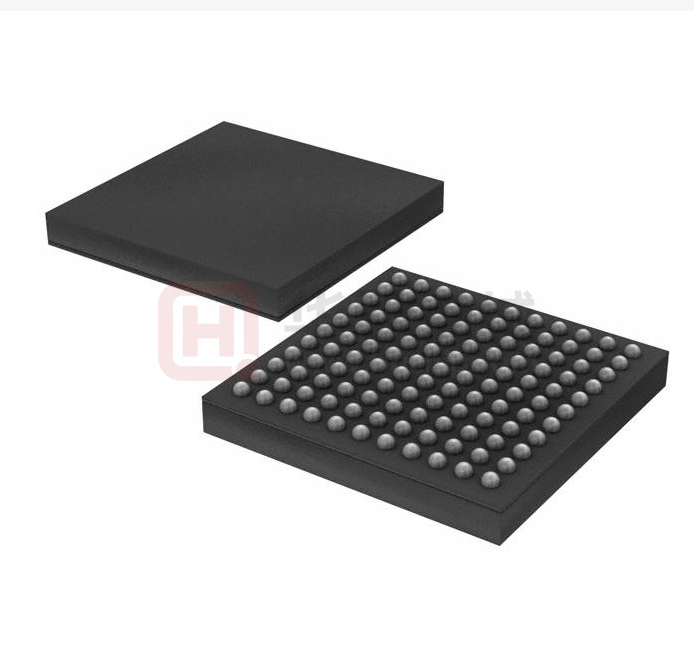
TC358774XBG
The TC358774XBG/TC358775XBG Functional Specification defines
operation of the DSISM to LVDS low power chip (or more abbreviated,
TC358775XBG chip). TC358775XBG is the follow-up chip of
TC358764XBG/ TC358765XBG, which:
P-VFBGA49-0505-0.65-001
Weight: 39 mg (Typ.)
1. Is pin compatible to TC358764XBG/TC358765XBG
2. Exhibit LVDS Tx block operates at 1.8V @135 MHz to reduce
TC358775XBG
operation power
3. Update 4-lane DSI Rx max bit rate @ 1 Gbps/lane to support
1920×1200×24 @60fps
4. Add STBY pin with to enable turning on VDDIO power first before
other power supplies.
P-VFBGA64-0606-0.65-001
Weight: 55 mg (Typ.)
The primary function of this chip is DSI-to-LVDS Bridge, enabling
video streaming output over DSI link to drive LVDS-compatible
display panels. The chip supports up to 1600×1200 24-bits per pixel resolution for single-link LVDS and
up to WUXGA (1920×1200 24-bits pixels) resolution for dual-link LVDS. As a secondary function, the
chip also supports an I2C Master which is controlled by the DSI link; this may be used as an interface to
any other control functions through I2C.
Features
● DSI Receiver
Configurable 1- up to 4-Data-Lane DSI Link with
Supports display up to 1600×1200 24-bits per
bi-directional support on Data Lane 0
Maximum bit rate of 1 Gbps/lane
Video input data formats:
- RGB565 16-bits per pixel
- RGB666 18-bits per pixel
- RGB666 loosely packed 24-bits per pixel
- RGB888 24-bits per pixel
Video frame size:
- Up to 1600×1200 24-bits per pixel resolution to
single-link LVDS display panel, limited by 135
MHz LVDS speed
- Up to WUXGA resolutions (1920×1200 24-bits
pixels) to dual-link LVDS display panel, limited by
4 Gbps DSI link speed
Supports Video Stream packets for video data
transmission.
Supports generic long packets for accessing the
chip's register set
Supports the path for Host to control the on-chip
I2C Master
● LVDS FPD Link Transmitter
Supports single-link or dual-link
Maximum pixel clock frequency of 135 MHz.
Maximum pixel clock speed of 135 MHz for singlelink or 270 MHz for dual-link
© 2014-2020
Toshiba Electronic Devices & Storage Corporation
pixel resolution for single-link, or up to 1920×1200
24-bits resolutions for dual-link
Supports the following pixel formats:
- RGB666 18-bits per pixel
- RGB888 24-bits per pixel
Features Toshiba Magic Square algorithm which
enables a RGB666 display panel to produce a
display quality almost equivalent to that of an
RGB888 24-bits panel
Flexible mapping of parallel data input bit ordering
Supports programmable clock polarity
Supports two power saving states
- Sleep state, when receiving DSI ULPS signaling
- Standby state, entered by STBY pin assertion
● System Operation
Host configures the chip through DSI link
Through DSI link, Host accesses the chip register
set using Generic Write and Read packets. One
Generic Long Write packet can write to multiple
contiguous register addresses
Includes an I2C Master function which is controlled
by Host through DSI link (multi-master is not
supported)
Power management features to save power
Configuration registers is also accessible through
I2C Slave interface
1 / 24
2020-01-15
Rev.1.91
�TC358774XBG/TC358775XBG
● Clock Source
LVDS pixel clock source is either from external
clock EXTCLK or derived from DSICLK.
A built-in PLL generates the high-speed LVDS
serializing clock requiring no external components
● Digital Input/Output Signals
All Digital Input signals are 3.3V tolerant
All Digital Output signals can output ranging from
1.8V to 3.3V depending on IO supply voltage
● Power supply
MIPI® DSI D-PHYSM: 1.2 V
LVDS PHY:
1.8 V
I/O:
1.8 V - 3.3V (all IO supply pins must
be same level)
Digital Core: 1.2 V
● Power Consumption
Power Down State is achieved by:
1. Reset asserted
2. EXTCLK not toggling
3. STBY = 0
4. DSI in ULPS Drive
● Packaging Information
BGA64 (0.65mm ball pitch)
- Supports DSI-RX 4-data-lanes + Dual-Link LVDSTX
- 6.0mm × 6.0mm × 1.0mm
BGA49 (0.65mm ball pitch)
- Supports DSI-RX 4-data-lanes + Single-Link
LVDS-TX
- 5.0mm × 5.0mm × 1.0mm
© 2014-2020
Toshiba Electronic Devices & Storage Corporation
2 / 24
2020-01-15
Rev.1.91
�TC358774XBG/TC358775XBG
Table of content
REFERENCE ....................................................................................................................................................... 7
1. Introduction....................................................................................................................................................... 9
1.1. Scope......................................................................................................................................................... 9
1.2. Purpose ..................................................................................................................................................... 9
2. Device Overview ............................................................................................................................................ 10
3. Features ......................................................................................................................................................... 11
4. Pin Layout ...................................................................................................................................................... 13
4.1. TC358775XBG BGA64 Pin-out Description ............................................................................................ 14
4.2. TC358775XBG BGA64 Pin Count Summary .......................................................................................... 15
4.3. TC358774XBG BGA49 Pin-out Description ............................................................................................ 16
4.4. TC358774XBG BGA49 Pin Count Summary .......................................................................................... 17
5. Package ......................................................................................................................................................... 18
6. Electrical characteristics................................................................................................................................. 20
6.1. Absolute Maximum Ratings..................................................................................................................... 20
6.2. Operating Conditions ............................................................................................................................... 20
6.3. DC Electrical Specification ...................................................................................................................... 21
6.3.1. Normal CMOS I/Os DC Specifications ....................................................................................................................... 21
6.3.2. DSI Differential I/Os DC Specifications....................................................................................................................... 21
6.3.2.1 LP Transmitter................................................................................................................................................................21
6.3.2.2 HS Receiver ...................................................................................................................................................................22
6.3.2.3 LP Receiver....................................................................................................................................................................22
6.3.3. LVDS Transmitter DC Specifications .......................................................................................................................... 22
7. Revision History ............................................................................................................................................. 23
RESTRICTIONS ON PRODUCT USE............................................................................................................... 24
3 / 24
2020-01-15
�TC358774XBG/TC358775XBG
Table of Figures
Figure 4.1
Figure 4.2
Figure 5.1
Figure 5.2
TC358775XBG Chip Pin Layout (BGA64 – Top View) .......................................................... 13
TC358774XBG Chip Pin Layout (BGA49 – Top View) .......................................................... 13
P-VFBGA64-0606-0.65-001 (TC358775XBG) Package Drawing.......................................... 18
P-VFBGA49-0505-0.65-001 (TC358774XBG) Package Drawing.......................................... 19
List of Tables
Table 4-1
Table 4-2
Table 5-1
Table 6-1
Table 6-2
Table 6-3
Table 6-4
Table 6-5
Table 6-6
Table 6-7
Table 7-1
TC358775XBG BGA64 Pin Count Summary .......................................................................... 15
BGA49 Pin Count Summary .................................................................................................... 17
Information Summary............................................................................................................... 19
Absolute Maximum Ratings ..................................................................................................... 20
Operating Conditions ............................................................................................................... 20
Normal CMOS IOs DC Specifications ..................................................................................... 21
DSI LP Transmitter DC Specifications..................................................................................... 21
DSI HS Receiver DC Specifications ........................................................................................ 22
DSI LP Receiver DC Specifications ......................................................................................... 22
LVDS Transmitter DC Specifications....................................................................................... 22
Revision History ....................................................................................................................... 23
4 / 24
2020-01-15
�TC358774XBG/TC358775XBG
● MIPI® is a registered service mark of MIPI Alliance, Inc. DSISM, DPISM and D-PHYSM are service marks
of MIPI Alliance, Inc.
● Other company names, product names, and service names may be trademarks of their respective
companies.
Copyright © 2005-2010 MIPI Alliance, Inc. All rights reserved.
All rights reserved. This material is reprinted with the permission of the MIPI Alliance, Inc. No part(s) of
this document may be disclosed, reproduced or used for any purpose other than as needed to support
the use of the products of Toshiba Cooperation and its subsidiaries and its affiliates
5 / 24
2020-01-15
�TC358774XBG/TC358775XBG
1
2
3
4
5
6
7
8
9
NOTICE OF DISCLAIMER
The material contained herein is not a license, either expressly or impliedly, to any IPR owned or controlled
by any of the authors or developers of this material or MIPI. The material contained herein is provided on
an “AS IS” basis and to the maximum extent permitted by applicable law, this material is provided AS IS
AND WITH ALL FAULTS, and the authors and developers of this material and MIPI hereby disclaim all
other warranties and conditions, either express, implied or statutory, including, but not limited to, any (if
any) implied warranties, duties or conditions of merchantability, of fitness for a particular purpose, of
accuracy or completeness of responses, of results, of workmanlike effort, of lack of viruses, and of lack of
negligence.
10
11
12
13
14
All materials contained herein are protected by copyright laws, and may not be reproduced, republished,
distributed, transmitted, displayed, broadcast or otherwise exploited in any manner without the express
prior written permission of MIPI Alliance. MIPI, MIPI Alliance and the dotted rainbow arch and all related
trademarks, tradenames, and other intellectual property are the exclusive property of MIPI Alliance and
cannot be used without its express prior written permission.
15
16
17
18
19
20
21
22
23
24
25
ALSO, THERE IS NO WARRANTY OF CONDITION OF TITLE, QUIET ENJOYMENT, QUIET
POSSESSION, CORRESPONDENCE TO DESCRIPTION OR NON-INFRINGEMENT WITH REGARD
TO THIS MATERIAL OR THE CONTENTS OF THIS DOCUMENT. IN NO EVENT WILL ANY
AUTHOR OR DEVELOPER OF THIS MATERIAL OR THE CONTENTS OF THIS DOCUMENT OR
MIPI BE LIABLE TO ANY OTHER PARTY FOR THE COST OF PROCURING SUBSTITUTE
GOODS OR SERVICES, LOST PROFITS, LOSS OF USE, LOSS OF DATA, OR ANY INCIDENTAL,
CONSEQUENTIAL, DIRECT, INDIRECT, OR SPECIAL DAMAGES WHETHER UNDER
CONTRACT, TORT, WARRANTY, OR OTHERWISE, ARISING IN ANY WAY OUT OF THIS OR
ANY OTHER AGREEMENT, SPECIFICATION OR DOCUMENT RELATING TO THIS MATERIAL,
WHETHER OR NOT SUCH PARTY HAD ADVANCE NOTICE OF THE POSSIBILITY OF SUCH
DAMAGES.
26
27
28
29
30
31
32
33
34
Without limiting the generality of this Disclaimer stated above, the user of the contents of this Document is
further notified that MIPI: (a) does not evaluate, test or verify the accuracy, soundness or credibility of the
contents of this Document; (b) does not monitor or enforce compliance with the contents of this Document;
and (c) does not certify, test, or in any manner investigate products or services or any claims of compliance
with the contents of this Document. The use or implementation of the contents of this Document may
involve or require the use of intellectual property rights ("IPR") including (but not limited to) patents,
patent applications, or copyrights owned by one or more parties, whether or not Members of MIPI. MIPI
does not make any search or investigation for IPR, nor does MIPI require or request the disclosure of any
IPR or claims of IPR as respects the contents of this Document or otherwise.
35
Questions pertaining to this document, or the terms or conditions of its provision, should be addressed to:
36
37
38
39
40
MIPI Alliance, Inc.
c/o IEEE-ISTO
445 Hoes Lane
Piscataway, NJ 08854
Attn: Board Secretary
This Notice of Disclaimer applies to all DSI input and processing paths related descriptions throughout this
document.
6 / 24
2020-01-15
�TC358774XBG/TC358775XBG
REFERENCE
1. MIPI D-PHY, “MIPI_D-PHY_specification_v01-00-00, May 14, 2009"
2. MIPI Alliance Specification for DSI version 1.01, Feb 2008
3. MIPI Alliance Specification for DPI version 2.0, Sep, 2005
7 / 24
2020-01-15
�TC358774XBG/TC358775XBG
Precautions and Usage Considerations Specific to Application Specific Standard Products and
General-Purpose Linear Ics
1.
CAUTION
Use an appropriate power supply fuse to ensure that a large current does not continuously flow in case
of over current and/or IC failure. The IC will fully break down when used under conditions that exceed its
absolute maximum ratings, when the wiring is routed improperly or when an abnormal pulse noise
occurs from the wiring or load, causing a large current to continuously flow and the breakdown can lead
smoke or ignition. To minimize the effects of the flow of a large current in case of breakdown,
appropriate settings, such as fuse capacity, fusing time and insertion circuit location, are required.
a. If your design includes an inductive load such as a motor coil, incorporate a protection circuit into
the design to prevent device malfunction or breakdown caused by the current resulting from the
inrush current at power ON or the negative current resulting from the back electromotive force at
power OFF. For details on how to connect a protection circuit such as a current limiting resistor or
back electromotive force adsorption diode, refer to individual IC datasheets or the IC databook. IC
breakdown may cause injury, smoke or ignition.
b. Use a stable power supply with ICs with built-in protection functions. If the power supply is unstable,
the protection function may not operate, causing IC breakdown. IC breakdown may cause injury,
smoke or ignition.
c. Carefully select external components (such as inputs and negative feedback capacitors) and load
components (such as speakers), for example, power amp and regulator.
If there is a large amount of leakage current such as input or negative feedback condenser, the IC
output DC voltage will increase. If this output voltage is connected to a speaker with low input
withstand voltage, overcurrent or IC failure can cause smoke or ignition. (The over current can
cause smoke or ignition from the IC itself.) In particular, please pay attention when using a Bridge
Tied Load (BTL) connection type IC that inputs output DC voltage to a speaker directly.
2.
Over current Protection Circuit
Over current protection circuits (referred to as current limiter circuits) do not necessarily protect ICs under all
circumstances. If the Over current protection circuits operate against the over current, clear the over current status
immediately.
Depending on the method of use and usage conditions, such as exceeding absolute maximum ratings can cause the
over current protection circuit to not operate properly or IC breakdown before operation. In addition, depending on the
method of use and usage conditions, if over current continues to flow for a long time after operation, the IC may generate
heat resulting in breakdown.
3.
Thermal Shutdown Circuit
Thermal shutdown circuits do not necessarily protect ICs under all circumstances. If the Thermal shutdown circuits
operate against the over temperature, clear the heat generation status immediately.
Depending on the method of use and usage conditions, such as exceeding absolute maximum ratings can cause the
thermal shutdown circuit to not operate properly or IC breakdown before operation.
4.
Heat Radiation Design
When using an IC with large current flow such as power amp, regulator or driver, please design the device so that heat
is appropriately radiated, not to exceed the specified junction temperature (TJ) at any time and condition. These ICs
generate heat even during normal use. An inadequate IC heat radiation design can lead to decrease in IC life,
deterioration of IC characteristics or IC breakdown. In addition, please design the device taking into considerate the
effect of IC heat radiation with peripheral components.
a. Mounting
5.
Installation to Heat Sink
Please install the power IC to the heat sink not to apply excessive mechanical stress to the IC. Excessive mechanical
stress can lead to package cracks, resulting in a reduction in reliability or breakdown of internal IC chip. In addition,
depending on the IC, the use of silicon rubber may be prohibited. Check whether the use of silicon rubber is prohibited
for the IC you intend to use, or not. For details of power IC heat radiation design and heat sink installation, refer to
individual technical datasheets or IC databooks.
a. Also please refer to ”RESTRICTIONS ON PRODUCT USE”.
8 / 24
2020-01-15
�TC358774XBG/TC358775XBG
1. Introduction
The TC358774XBG/TC358775XBG Functional Specification defines operation of the DSI TO LVDS low
power chip (or more abbreviated, TC358775XBG chip). TC358775XBG is the follow-up chip of
TC358764XBG/ TC358765XBG, which:
1.
2.
3.
4.
Is pin compatible to TC358764XBG/TC358765XBG
Exhibit LVDS Tx block operates at 1.8V @135 MHz to reduce operation power
Update 4-lane DSI Rx max bit rate @ 1 Gbps/lane to support 1920 × 1200 × 24 @60fps
Add STBY pin with to enable turning on VDDIO power first before other power supplies.
The primary function of this chip is DSI-to-LVDS Bridge, enabling video streaming output over DSI link
to drive LVDS-compatible display panels. The chip supports up to 1600×1200 24-bits per pixel
resolution for single-link LVDS and up to WUXGA (1920×1200 24-bits pixels) resolution for dual-link
LVDS. As a secondary function, the chip also supports an I2C Master which is controlled by the DSI link;
this may be used as an interface to any other control functions through I2C.
The chip can be configured through the DSI link by sending write register commands through DSI
Generic Long Write-packets. It can also be configured through the I2C Slave interface. I2C slave
address of TC358774XBG/TC358775XBG is 8'b0001_111X, where X = 0/1 for write/read to/from
TC358775XBG operation.
This specification provides description of two product versions:
TC358774XBG:
In BGA49 package, it supports DSI-RX with up to 4 data lanes, and outputs to Single-Link LVDS.
TC358775XBG:
In BGA64 package, it supports DSI-RX with up to 4 data lanes, and outputs to Dual-Link LVDS.
1.1. Scope
This document details the operation of the chip, description of each major function that the chip
supports, description of the configuration register set, and includes pinout, package, and electrical
characteristics information.
1.2. Purpose
This document serves as the vehicle for exchanging detailed technical information of the
TC358774XBG/TC358775XBG chip and its usage within the target application systems at the customer
side. It also serves as the chip functional specification for design implementation and verification.
9 / 24
2020-01-15
�TC358774XBG/TC358775XBG
2. Device Overview
The TC358774XBG/TC358775XBG chip functions primarily as a DSI-to-LVDS communication protocol
bridge, enabling video streaming from a Host processor over DSI link to drive LVDS-compatible display
panels. In other words, the chip receives video stream input through its DSI receiver (DSI-RX), buffers
the received pixel data in a buffer, and then re-transmits the video stream out through the LVDS
transmitter.
As a secondary function, the chip also ports an I2C Master which is controlled by the DSI link; this may
be used as a programming interface to other peripherals in the system.
The chip is configured through the DSI link. Alternatively, it can optionally be configured through the I2C
Slave interface; in such case, the I2C Master function would be disabled.
The reference video pixel clock for the LVDS link is sourced either from an external clock via input pin
EXTCLK or derived from DSICLK. The chip integrates a PLL which synthesizes the high-speed clock for
use solely to serialize video data over the LVDS link.
The DSI-RX receiver supports from 1- to 4-Lane configurations at bit rate up to 1 Gbps per lane. Host
can transmit video in video mode. In video mode, Host controls video timing by sending video frame
and line sync events together with video pixel data; video data transmission can be burst or non-burst.
Since the chip integrates only 1024-pixel of video buffer, Host still has to take care of transmitting pixel
data at appropriate video line time in order to avoid buffer overflow (or underflow).
The LVDS transmitter supports a clock frequency of up to 135 MHz for either single- or dual-link.
The chip supports power management to conserve power when its functions are not in use. Host
manages the chip's power consumption states by using ULPS signaling over DSI link and/or STBY pin.
10 / 24
2020-01-15
�TC358774XBG/TC358775XBG
3. Features
● DSI Receiver
Configurable 1- up to 4-Data-Lane DSI Link with bi-directional support on Data Lane 0
Maximum bit rate of 1 Gbps/lane
Video input data formats:
- RGB565 16-bits per pixel
- RGB666 18-bits per pixel
- RGB666 loosely packed 24-bits per pixel
- RGB888 24-bits per pixel
Video frame size:
- Up to 1600×1200 24-bits per pixel resolution to single-link LVDS display panel, limited by 135
MHz LVDS speed
- Up to WUXGA resolutions (1920×1200 24-bits pixels) to dual-link LVDS display panel, limited
by 4 Gbps DSI link speed
Supports Video Stream packets for video data transmission
Supports generic long packets for accessing the chip's register set
Supports the path for Host to control the on-chip I2C Master
● LVDS FPD Link Transmitter
Supports single-link or dual-link
Maximum pixel clock frequency of 135 MHz.
Maximum pixel clock speed of 135 MHz for single-link or 270 MHz for dual-link
Supports display up to 1600×1200 24-bits per pixel resolution for single-link, or up to 1920×1200
24-bits resolutions for dual-link
Supports the following pixel formats:
- RGB666 18-bits per pixel
- RGB888 24-bits per pixel
Features Toshiba Magic Square algorithm which enables a RGB666 display panel to produce a
display quality almost equivalent to that of an RGB888 24-bits panel
Flexible mapping of parallel data input bit ordering
Supports programmable clock polarity
Supports two power saving states
- Sleep state, when receiving DSI ULPS signaling
- Standby state, entered by STBY pin assertion
● System Operation
Host configures the chip through DSI link.
Through DSI link, Host accesses the chip register set using Generic Write and Read packets. One
Generic Long Write packet can write to multiple contiguous register addresses.
Includes an I2C Master function which is controlled by Host through DSI link (multi-master is not
supported)
Power management features to save power
Configuration registers is also accessible through I2C Slave interface.
● Clock Source
LVDS pixel clock source is either from external clock EXTCLK or derived from DSICLK.
A built-in PLL generates the high-speed LVDS serializing clock requiring no external components
● Digital Input/Output Signals
All Digital Input signals are 3.3V tolerant.
All Digital Output signals can output ranging from 1.8V to 3.3V depending on IO supply voltage.
11 / 24
2020-01-15
�TC358774XBG/TC358775XBG
● Power supply
MIPI DSI D-PHY: 1.2 V
LVDS PHY:
1.8 V
I/O:
1.8 V - 3.3V (all IO supply pins must be same level)
Digital Core: 1.2 V
● Power Consumption
Power Down State is achieved by:
1.
2.
3.
4.
Reset asserted
EXTCLK not toggling
STBY = 0
DSI in ULPS Drive
Reduced Mode
720×480×18
@26 MHz
1366×768×18
@85 MHz
1920×1080×18
Dual Link
@74MHz
Power Down
VDDC
VDDS
DSI
LVDS
VDDC
VDDIO
VDD1
LVDS1.2
LVDS1.8
1.2
1.8
1.2
1.2
1.8
V
8.60
0.11
8.40
3.60
10.00
mA
10.32
0.20
10.08
4.32
18.00
17.2
0.13
14.6
8.3
11.1
20.64
0.23
17.52
9.96
19.98
18.57
0.092
19.77
8.123
22.4
22.28
0.17
23.72
9.75
40.32
0.03
0.01
0.02
0.01
0.02
0.04
0.02
0.02
0.01
0.04
TOTAL
Power
42.92
Unit
mW
mA
68.33
mW
mA
96.24
mW
mA
0.09
mW
● Packaging Information
BGA64 (0.65 mm ball pitch)
- Supports DSI-RX 4-data-lanes + Dual-Link LVDS-TX
- 6.0 mm × 6.0 mm × 1.0 mm
BGA49 (0.65 mm ball pitch)
- Supports DSI-RX 4-data-lanes + Single-Link LVDS-TX
- 5.0 mm × 5.0 mm × 1.0 mm
12 / 24
2020-01-15
�TC358774XBG/TC358775XBG
4. Pin Layout
A1
A2
A3
A4
A5
A6
A7
A8
VSS_LVDS2_12
LVTX2AN
LVTX2BN
LVTX2CN
LVTX2DN
LVTX2EN
VSS_LVDS2_18
VSS_LVDS1_12
B1
B2
B3
B4
B5
B6
B7
B8
VDD_LVDS2_12
LVTX2AP
LVTX2BP
LVTX2CP
LVTX2DP
LVTX2EP
VDD_LVDS2_18
VDD_LVDS1_12
C5
C6
C1
C2
C3
C4
VSSIO
VDDIO
STBY
GPIO3
VDD_LVDS2_18 VSS_LVDS2_18
C7
C8
LVTX1AP
LVTX1AN
D1
D2
D3
D4
D5
D6
D7
D8
EXTCLK
GPIO2
GPIO1
RESX
TM
VDD_LVDS1_18
LVTX1BP
LVTX1BN
E1
E2
E3
E4
E5
E6
E7
E8
VSSC
VDDC
GPIO0
VDDC
VSSC
VSS_LVDS1_18
LVTX1CP
LVTX1CN
F1
F2
F3
F4
F5
F6
F7
F8
VSSIO
VDDIO
VDD_MIPI
VSS_MIPI
VSS_MIPI
VDD_MIPI
LVTX1DP
LVTX1DN
G1
G2
G3
G4
G5
G6
G7
G8
I2C_SCL
DSRXD0P
DSRXD1P
DSRXCP
DSRXD2P
DSRXD3P
LVTX1EP
LVTX1EN
H7
H8
H1
H2
H3
H4
H5
H6
I2C_SDA
DSRXD0M
DSRXD1M
DSRXCM
DSRXD2M
DSRXD3M
Figure 4.1
VDD_LVDS1_18 VSS_LVDS1_18
TC358775XBG Chip Pin Layout (BGA64 – Top View)
A1
A2
A3
A4
A5
A6
A7
VSSIO
VDDIO
RESX
GPIO0
VSSC
VDDC
VSSC
B1
B2
B3
B4
B5
B6
B7
EXTCLK
VDDC
VSSC
TM
VDD_LVDS1_12
LVTX1AP
LVTX1AN
C1
C2
C3
C4
C5
C6
C7
I2C_SDA
GPIO3
GPIO2
GPIO1
VSS_LVDS1_12
LVTX1BP
LVTX1BN
D1
D2
D3
D4
D5
D6
D7
I2C_SCL
STBY
VSS_MIPI
VDD_MIPI
VSS_LVDS1_18
LVTX1CP
LVTX1CN
E1
E2
E3
E4
E5
E6
E7
VDDIO
VSSIO
VSS_MIPI
VDD_MIPI
VDD_LVDS1_18
LVTX1DP
LVTX1DN
F1
F2
F3
F4
F5
F6
F7
DSRXD1P
DSRXCP
DSRXD2P
DSRXD3P
LVTX1EP
LVTX1EN
G6
G7
DSRXD0P
G1
G2
G3
G4
G5
DSRXD0M
DSRXD1M
DSRXCM
DSRXD2M
DSRXD3M
Figure 4.2
VDD_LVDS1_18 VSS_LVDS1_18
TC358774XBG Chip Pin Layout (BGA49 – Top View)
13 / 24
2020-01-15
�TC358774XBG/TC358775XBG
4.1. TC358775XBG BGA64 Pin-out Description
Group
DSI-RX IF
1st-Link
LVDS-TX
IF
2nd-Link
LVDS-TX
IF
I2C IF
GPIO
SYSTEM
Pin Name
IO Type
Pin Cnt.
Description
DSRXCP
DSRXCM
DSRXD0P
DSRXD0M
DSRXD1P
DSRXD1M
DSRXD2P
DSRXD2M
DSRXD3P
DSRXD3M
VDD_MIPI
VSS_MIPI
LVTX1AP
LVTX1AN
LVTX1BP
LVTX1BN
LVTX1CP
LVTX1CN
LVTX1DP
LVTX1DN
LVTX1EP
LVTX1EN
VDD_LVDS1_18
VSS_LVDS1_18
VDD_LVDS1_12
VSS_LVDS1_12
LVTX2AP
LVTX2AN
LVTX2BP
LVTX2BN
LVTX2CP
LVTX2CN
LVTX2DP
LVTX2DN
LVTX2EP
LVTX2EN
VDD_LVDS2_18
VSS_LVDS2_18
VDD_LVDS2_12
VSS_LVDS2_12
I2C_SCL
I2C_SDA
GPIO[3:0]
RESX
EXTCLK
STBY
TM
VDDIO
VSSIO
VDDC
VSSC
DSI-PHY
DSI-PHY
DSI-PHY
DSI-PHY
DSI-PHY
DSI-PHY
DSI-PHY
DSI-PHY
DSI-PHY
DSI-PHY
Power
Ground
LVDS-PHY
LVDS-PHY
LVDS-PHY
LVDS-PHY
LVDS-PHY
LVDS-PHY
LVDS-PHY
LVDS-PHY
LVDS-PHY
LVDS-PHY
Power
Ground
Power
Ground
LVDS-PHY
LVDS-PHY
LVDS-PHY
LVDS-PHY
LVDS-PHY
LVDS-PHY
LVDS-PHY
LVDS-PHY
LVDS-PHY
LVDS-PHY
Power
Ground
Power
Ground
S-OD
S-OD
N-PD
N-PD
N-PD
N
N-PD
Power
Ground
Power
Ground
1
1
1
1
1
1
1
1
1
1
2
2
1
1
1
1
1
1
1
1
1
1
2
2
1
1
1
1
1
1
1
1
1
1
1
1
2
2
1
1
1
1
4
1
1
1
1
2
2
2
2
DSI clock signal - positive
DSI clock signal - negative
DSI data lane 0 - positive
DSI data lane 0 - negative
DSI data lane 1 - positive
DSI data lane 1 - negative
DSI data lane 2 - positive
DSI data lane 2 - negative
DSI data lane 3 - positive
DSI data lane 3 - negative
MIPI Analog Power Supply
MIPI Analog Ground
LVDS first-link data channel A - positive
LVDS first-link data channel A - negative
LVDS first-link data channel B - positive
LVDS first-link data channel B - negative
LVDS first-link data channel C - positive
LVDS first-link data channel C - negative
LVDS first-link data channel D (Clock) - positive
LVDS first-link data channel D (Clock) - negative
LVDS first-link data channel E - positive
LVDS first-link data channel E - negative
First-link LVDS 1.8V Power Supply
First-link LVDS 1.8V Ground
First-link LVDS 1.2V Power Supply
First-link LVDS 1.2V Ground
LVDS second-link data channel A - positive
LVDS second-link data channel A - negative
LVDS second-link data channel B - positive
LVDS second-link data channel B - negative
LVDS second-link data channel C - positive
LVDS second-link data channel C - negative
LVDS second-link data channel D (Clock) - positive
LVDS second-link data channel D (Clock) -negative
LVDS second-link data channel E - positive
LVDS second-link data channel E - negative
Second-link LVDS 1.8V Power Supply
Second-link LVDS 1.8V Ground
Second-link LVDS 1.2V Power Supply
Second-link LVDS 1.2V Ground
I2C Master or Slave interface clock signal
I2C Master or Slave interface data signal
GPIO bits 3-0
Hardware reset, low active
External pixel clock source
Standby pin, low active
Test mode select
IO Power Supply
IO Ground
Digital Core Power Supply
Digital Core Ground
14 / 24
Power
Supply
Voltage
1.2 V
1.2 V
1.2 V
1.2 V
1.2 V
1.2 V
1.2 V
1.2 V
1.2 V
1.2 V
1.2 V
GND
1.8 V
1.8 V
1.8 V
1.8 V
1.8 V
1.8 V
1.8 V
1.8 V
1.8 V
1.8 V
1.8 V
GND
1.2 V
GND
1.8 V
1.8 V
1.8 V
1.8 V
1.8 V
1.8 V
1.8 V
1.8 V
1.8 V
1.8 V
1.8 V
GND
1.2 V
GND
1.8V - 3.3V
1.8V - 3.3V
1.8V - 3.3V
1.8V - 3.3V
1.8V - 3.3V
1.8V - 3.3V
1.8V - 3.3V
1.8V - 3.3V
GND
1.2 V
GND
2020-01-15
�TC358774XBG/TC358775XBG
Buffer Type Abbreviation:
N:
Normal IO
N-PD :
Normal IO with Pull Down
S-OD:
Pseudo open-drain output, schmitt input
DSI-PHY:
front-end analog IO for DSI
LVDS-PHY: front-end analog IO for LVDS
4.2. TC358775XBG BGA64 Pin Count Summary
Table 4-1
TC358775XBG BGA64 Pin Count Summary
Group Name
Pin Count
DSI-RX IF
1st-Link/2nd Link
LVDS-TX IF
I2C IF
GPIO
SYSTEM
Total Pin Count
14
Include DSI Power & Ground
32
Include LVDS Power & Ground
2
4
12
64
15 / 24
Note
-
2020-01-15
�TC358774XBG/TC358775XBG
4.3. TC358774XBG BGA49 Pin-out Description
Group
DSI-RX IF
LVDS-TX
IF
I2C IF
GPIO
SYSTEM
Pin Name
IO Type
Pin Cnt.
DSRXCP
DSRXCM
DSRXD0P
DSRXD0M
DSRXD1P
DSRXD1M
DSRXD2P
DSRXD2M
DSRXD3P
DSRXD3M
VDD_MIPI
VSS_MIPI
LVTX1AP
LVTX1AN
LVTX1BP
LVTX1BN
LVTX1CP
LVTX1CN
LVTX1DP
LVTX1DN
LVTX1EP
LVTX1EN
VDD_LVDS1_18
VSS_LVDS1_18
VDD_LVDS1_12
VSS_LVDS1_12
I2C_SCL
I2C_SDA
GPIO[3:0]
RESX
EXTCLK
STBY
TM
VDDIO
VSSIO
VDDC
VSSC
DSI-PHY
DSI-PHY
DSI-PHY
DSI-PHY
DSI-PHY
DSI-PHY
DSI-PHY
DSI-PHY
DSI-PHY
DSI-PHY
Power
Ground
LVDS-PHY
LVDS-PHY
LVDS-PHY
LVDS-PHY
LVDS-PHY
LVDS-PHY
LVDS-PHY
LVDS-PHY
LVDS-PHY
LVDS-PHY
Power
Ground
Power
Ground
S-OD
S-OD
N-PD
N-PD
N-PD
N
N-PD
Power
Ground
Power
Ground
1
1
1
1
1
1
1
1
1
1
2
2
1
1
1
1
1
1
1
1
1
1
2
2
1
1
1
1
4
1
1
1
1
2
2
2
3
Description
DSI clock signal - positive
DSI clock signal - negative
DSI data lane 0 - positive
DSI data lane 0 - negative
DSI data lane 1 - positive
DSI data lane 1 - negative
DSI data lane 2 - positive
DSI data lane 2 - negative
DSI data lane 3 - positive
DSI data lane 3 - negative
MIPI Analog Power Supply
MIPI Analog Ground
LVDS first-link data channel A - positive
LVDS first-link data channel A - negative
LVDS first-link data channel B - positive
LVDS first-link data channel B - negative
LVDS first-link data channel C - positive
LVDS first-link data channel C - negative
LVDS first-link data channel D (Clock) - positive
LVDS first-link data channel D (Clock) - negative
LVDS first-link data channel E - positive
LVDS first-link data channel E - negative
First-link LVDS 1.8V Power Supply
First-link LVDS 1.8V Ground
First-link LVDS 1.2V Power Supply
First-link LVDS 1.2V Ground
I2C Master or Slave interface clock signal
I2C Master or Slave interface data signal
GPIO bits 3-0
Hardware reset, low active
External pixel clock source
Standby pin, low active
Test mode select
IO Power Supply
IO Ground
Digital Core Power Supply
Digital Core Ground
Power Supply
Voltage
1.2 V
1.2 V
1.2 V
1.2 V
1.2 V
1.2 V
1.2 V
1.2 V
1.2 V
1.2 V
1.2 V
GND
1.8 V
1.8 V
1.8 V
1.8 V
1.8 V
1.8 V
1.8 V
1.8 V
1.8 V
1.8 V
1.8 V
GND
1.2 V
GND
1.8V - 3.3V
1.8V - 3.3V
1.8V - 3.3V
1.8V - 3.3V
1.8V - 3.3V
1.8V - 3.3V
1.8V - 3.3V
1.8V - 3.3V
GND
1.2 V
GND
Buffer Type Abbreviation:
N:
Normal IO
N-PD:
Normal IO
S-OD:
Pseudo open-drain output, schmitt input
DSI-PHY:
front-end analog IO for DSI
LVDS-PHY: front-end analog IO for LVDS
16 / 24
2020-01-15
�TC358774XBG/TC358775XBG
4.4. TC358774XBG BGA49 Pin Count Summary
Table 4-2 BGA49 Pin Count Summary
Group Name
Pin Count
DSI-RX IF
LVDS-TX IF
I2C IF
GPIO
SYSTEM
Total Pin Count
14
16
2
4
13
49
Note
Include DSI Power & Ground
Include LVDS Power & Ground
-
17 / 24
2020-01-15
�TC358774XBG/TC358775XBG
5. Package
Weight: 55 mg (Typ.)
Figure 5.1
P-VFBGA64-0606-0.65-001 (TC358775XBG) Package Drawing
18 / 24
2020-01-15
�TC358774XBG/TC358775XBG
“ Unit: mm “
Weight: 39mg (Typ.)
Figure 5.2
P-VFBGA49-0505-0.65-001 (TC358774XBG) Package Drawing
Table 5-1
Package Type
Ball Diameter
Ball Pitch (e)
Edge Ball center to center (E1 × D1)
Body Size (E × D)
Thickness (A)
Information Summary
TC358775XBG
Package
TC358774XBG
Package
VFBGA
0.3 mm
0.65 mm
4.55 mm × 4.55 mm
6 mm × 6 mm
1 mm
VFBGA
0.3 mm
0.65 mm
3.90 mm × 3.90 mm
5 mm × 5 mm
1 mm
19 / 24
2020-01-15
�TC358774XBG/TC358775XBG
6. Electrical characteristics
6.1. Absolute Maximum Ratings
Operating ambient Temperature range: Ta = -30°C to +85°C
All voltage values, except differential I/O bus voltages, are with respect to network ground terminal.
Table 6-1
Parameter
Supply voltage
(1.8V – Digital IO)
Supply voltage
(1.2V – Digital Core)
Supply voltage
(1.2V – MIPI DSI PHY)
Supply voltage
(1.8V – LVDS PHY)
Absolute Maximum Ratings
Symbol
Rating
Unit
VDDIO
-0.3 to +3.9
V
VDDC
-0.3 to +1.8
V
VDD_MIPI
-0.3 to +1.8
V
VDD_LVDS1_18,
VDD_LVDS2_18
-0.3 to +LVDS_18+0.3
V
VDD_LVDS1_12
VDD_LVDS2_12
-0.3 to +1.8
V
VIN_DSI
-0.3 to VDD_MIPI+0.3
V
VOUT_DSI
-0.3 to VDD_MIPI+0.3
V
VIN_IO
-0.3 to VDDIO+0.3
V
VOUT_IO
-0.3 to VDDIO+0.3
V
VOUT_LVDS
-0.3 to VDD_LVDS_18+0.3
V
Supply voltage
(1.2V – LVDS PHY)
Input voltage
(DSI I/O)
Output voltage
(DSI I/O)
Input voltage
(Digital IO)
Output voltage
(Digital IO)
Output voltage
(LVDS Driver)
6.2. Operating Conditions
Table 6-2
Parameter
Operating Conditions
Symbol
Min
Typ.
Max
Unit
Supply voltage (1.8V – Digital IO)
VDDIO
1.7
1.8
1.9
V
Supply voltage (3.3V – Digital IO)
VDDIO
3.0
3.3
3.6
V
Supply voltage (1.2V – Digital Core)
VDDC
1.1
1.2
1.3
V
Supply voltage (1.2V – LVDS PHY)
VDD_LVDS_12
1.1
1.2
1.3
V
Supply voltage (1.8V – LVDS PHY)
VDD_LVDS_18
1.7
1.8
1.9
V
VDD_MIPI
1.1
1.2
1.3
V
Ta
-30
+25
+85
°C
Supply voltage (1.2V – MIPI-DSI PHY)
Operating temperature (ambient
temperature with voltage applied)
20 / 24
2020-01-15
�TC358774XBG/TC358775XBG
6.3. DC Electrical Specification
All typical values are at normal operating conditions unless otherwise specified.
6.3.1. Normal CMOS I/Os DC Specifications
Table 6-3 Normal CMOS IOs DC Specifications
Parameter – CMOS I/Os
Input voltage, High level Input
Note1
Input voltage, Low level Input
Note1
Input voltage High level
CMOS Schmitt Trigger
Symbol
Conditions
Min
Typ.
Max
Unit
VIH
-
0.7
VDDIO
-
VDDIO
V
VIL
-
0
-
0.3
VDDIO
V
VIHS
-
0.7
VDDIO
-
VDDIO
V
VILS
-
0
-
0.3
VDDIO
V
VOL
IOL = 2mA
0
-
0.2
VDDIO
V
IILH1
(Note3)
VIN = +VDDIO, VDDIO = 3.6V
-10
-
10
µA
IILH2
(Note3)
VIN = +VDDIO, VDDIO = 3.6V
-
-
100
µA
IILL1
(Note4)
VIN = 0V, VDDIO = 3.6V
-10
-
10
µA
Note 1, 2
Input voltage Low level
CMOS Schmitt Trigger
Note 1, 2
Output voltage, Low level
Note1, 2
Input leakage current, High level
on Normal pin
Input leakage current, High level
on Pull-down I/O pin
Input leakage current, Low level
On Normal pin or Pull-down I/O
pin
Note1:
Note2:
Note3:
Note4:
Each power source is operating within recommended operating condition.
Current output value is specified to each IO buffer individually. Output voltage changes with
output current value.
Normal I/O pin applied VDDIO supply voltage to Vin (input voltage).
Normal pin, or Pull-down I/O pin applied VSSIO (0V) to Vin (input voltage).
6.3.2. DSI Differential I/Os DC Specifications
6.3.2.1 LP Transmitter
The low power transmitter is used for driving the lines in all low-power operating modes. The DC
characteristics of the LP transmitter are given below.
Table 6-4 DSI LP Transmitter DC Specifications
Parameter
Symbol
Min
Typ.
Max
Unit
Thevenin output low level
VOL
-50
-
50
mV
Output impedance of the LP transmitter
ZOLP
110
-
-
Ω
21 / 24
2020-01-15
�TC358774XBG/TC358775XBG
6.3.2.2 HS Receiver
The high-speed receiver is a differential line receiver with a switch able parallel input termination. It is
used to receive data during high speed transmission from the host. The DC characteristics of the HS
receiver are given below.
Table 6-5 DSI HS Receiver DC Specifications
Parameter
Symbol
Min
Typ.
Max
Unit
Common-mode voltage HS receive mode
VCMRX(DC)
70
-
330
mV
Differential input high threshold
VIDTH
-
-
70
mV
Differential input low threshold
VIDTL
-70
-
-
mV
Single-ended input high voltage
VIHHS
-
-
460
mV
Single-ended input low voltage
Single-ended threshold for HS
termination enable
Differential input impedance
VILHS
-40
-
-
mV
VTERM-EN
-
-
450
mV
ZID
80
100
125
Ω
6.3.2.3 LP Receiver
The low-power receiver is used to detect the Low-Power state on each pin. It is used to receive data
during low speed transmission from the host. The DC characteristics of the LP receiver are given below.
Table 6-6 DSI LP Receiver DC Specifications
Parameter
Symbol
Min
Typ.
Max
Unit
Logic 1 input voltage
VIH
880
-
-
mV
Logic 0 input voltage
VIL
-
-
550
mV
6.3.3. LVDS Transmitter DC Specifications
Table 6-7
Parameter
LVDS Transmitter DC Specifications
Symbol
Conditions
Min
Typ.
Max Unit
Output differential voltage Normal
|VOD|
RLOAD = 100Ω±1%
150
300
450
mV
Output differential voltage Reduced
|VOD|
RLOAD = 100Ω±1%
115
180
300
mV
Change in |VOD| between “0”and “1”
ΔVOD
RLOAD = 100Ω±1%
-
-
30
mV
VOS
RLOAD = 100Ω±1%
800
900
1000
mV
ΔVOS
RLOAD = 100Ω±1%
-
-
25
mV
Output offset voltage
Change in VOS between “0”and “1”
Output current
Isab
Driver shorted together
-
-
12
mA
Output current
Isab, Isb
Driver shorted to ground
-
-
30
mA
22 / 24
2020-01-15
�TC358774XBG/TC358775XBG
7. Revision History
Table 7-1 Revision History
Revision
Date
Description
1.5
2014-04-10
Newly released
1.5.1
2016-02-18
Package name and its drawing is modified.
• TC358774XBG -> P-VFBGA49-0505-0.65-001
• TC358775XBG -> P-VFBGA64-0606-0.65-001
1.7b
2017-07-01
Added Table number as Table 6-7.
Changed header, footer and the last page.
Changed corporate name.
1.9
2019-01-18
Modified descriptions of services mark and trademark.
Added service marks.
Corrected typos.
Modified Note numbers in Table 6-3.
Corrected weights of TC358774XBG and TC358775XBG.
Revised the last page “RESTRICTIONS ON PRODUCT USE”
and added URL.
1.9.1
2020-01-15
IO type Correction in Section 4.1 and 4.3
IILL2 spec. to be deleted from Table 6-3 Normal CMOS IOs DC
Specifications
23 / 24
2020-01-15
�TC358774XBG/TC358775XBG
RESTRICTIONS ON PRODUCT USE
Toshiba Corporation and its subsidiaries and affiliates are collectively referred to as “TOSHIBA”.
Hardware, software and systems described in this document are collectively referred to as “Product”.
• TOSHIBA reserves the right to make changes to the information in this document and related Product without notice.
• This document and any information herein may not be reproduced without prior written permission from TOSHIBA. Even with
TOSHIBA's written permission, reproduction is permissible only if reproduction is without alteration/omission.
• Though TOSHIBA works continually to improve Product's quality and reliability, Product can malfunction or fail. Customers are
responsible for complying with safety standards and for providing adequate designs and safeguards for their hardware, software and
systems which minimize risk and avoid situations in which a malfunction or failure of Product could cause loss of human life, bodily
injury or damage to property, including data loss or corruption. Before customers use the Product, create designs including the
Product, or incorporate the Product into their own applications, customers must also refer to and comply with (a) the latest versions of
all relevant TOSHIBA information, including without limitation, this document, the specifications, the data sheets and application notes
for Product and the precautions and conditions set forth in the "TOSHIBA Semiconductor Reliability Handbook" and (b) the
instructions for the application with which the Product will be used with or for. Customers are solely responsible for all aspects of their
own product design or applications, including but not limited to (a) determining the appropriateness of the use of this Product in such
design or applications; (b) evaluating and determining the applicability of any information contained in this document, or in charts,
diagrams, programs, algorithms, sample application circuits, or any other referenced documents; and (c) validating all operating
parameters for such designs and applications. TOSHIBA ASSUMES NO LIABILITY FOR CUSTOMERS' PRODUCT DESIGN OR
APPLICATIONS.
• PRODUCT IS NEITHER INTENDED NOR WARRANTED FOR USE IN EQUIPMENTS OR SYSTEMS THAT REQUIRE
EXTRAORDINARILY HIGH LEVELS OF QUALITY AND/OR RELIABILITY, AND/OR A MALFUNCTION OR FAILURE OF WHICH
MAY CAUSE LOSS OF HUMAN LIFE, BODILY INJURY, SERIOUS PROPERTY DAMAGE AND/OR SERIOUS PUBLIC IMPACT
("UNINTENDED USE"). Except for specific applications as expressly stated in this document, Unintended Use includes, without
limitation, equipment used in nuclear facilities, equipment used in the aerospace industry, lifesaving and/or life supporting medical
equipment, equipment used for automobiles, trains, ships and other transportation, traffic signaling equipment, equipment used to
control combustions or explosions, safety devices, elevators and escalators, and devices related to power plant. IF YOU USE
PRODUCT FOR UNINTENDED USE, TOSHIBA ASSUMES NO LIABILITY FOR PRODUCT. For details, please contact your
TOSHIBA sales representative or contact us via our website.
• Do not disassemble, analyze, reverse-engineer, alter, modify, translate or copy Product, whether in whole or in part.
• Product shall not be used for or incorporated into any products or systems whose manufacture, use, or sale is prohibited under any
applicable laws or regulations.
• The information contained herein is presented only as guidance for Product use. No responsibility is assumed by TOSHIBA for any
infringement of patents or any other intellectual property rights of third parties that may result from the use of Product. No license to
any intellectual property right is granted by this document, whether express or implied, by estoppel or otherwise.
• ABSENT A WRITTEN SIGNED AGREEMENT, EXCEPT AS PROVIDED IN THE RELEVANT TERMS AND CONDITIONS OF SALE
FOR PRODUCT, AND TO THE MAXIMUM EXTENT ALLOWABLE BY LAW, TOSHIBA (1) ASSUMES NO LIABILITY
WHATSOEVER, INCLUDING WITHOUT LIMITATION, INDIRECT, CONSEQUENTIAL, SPECIAL, OR INCIDENTAL DAMAGES OR
LOSS, INCLUDING WITHOUT LIMITATION, LOSS OF PROFITS, LOSS OF OPPORTUNITIES, BUSINESS INTERRUPTION AND
LOSS OF DATA, AND (2) DISCLAIMS ANY AND ALL EXPRESS OR IMPLIED WARRANTIES AND CONDITIONS RELATED TO
SALE, USE OF PRODUCT, OR INFORMATION, INCLUDING WARRANTIES OR CONDITIONS OF MERCHANTABILITY, FITNESS
FOR A PARTICULAR PURPOSE, ACCURACY OF INFORMATION, OR NONINFRINGEMENT.
• Do not use or otherwise make available Product or related software or technology for any military purposes, including without
limitation, for the design, development, use, stockpiling or manufacturing of nuclear, chemical, or biological weapons or missile
technology products (mass destruction weapons). Product and related software and technology may be controlled under the
applicable export laws and regulations including, without limitation, the Japanese Foreign Exchange and Foreign Trade Law and the
U.S. Export Administration Regulations. Export and re-export of Product or related software or technology are strictly prohibited
except in compliance with all applicable export laws and regulations.
• Please contact your TOSHIBA sales representative for details as to environmental matters such as the RoHS compatibility of
Product. Please use Product in compliance with all applicable laws and regulations that regulate the inclusion or use of controlled
substances, including without limitation, the EU RoHS Directive. TOSHIBA ASSUMES NO LIABILITY FOR DAMAGES OR LOSSES
OCCURRING AS A RESULT OF NONCOMPLIANCE WITH APPLICABLE LAWS AND REGULATIONS.
https://toshiba.semicon-storage.com/
24 / 24
2020-01-15
�