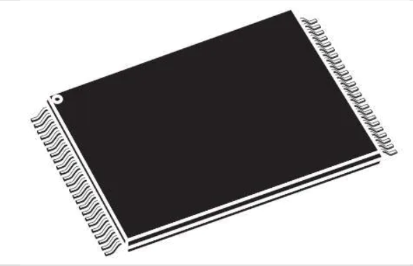
TC58NVG0S3HTA00
MOS DIGITAL INTEGRATED CIRCUIT SILICON GATE CMOS
1G BIT (128M × 8 BIT) CMOS NAND E2PROM
DESCRIPTION
The TC58NVG0S3HTA00 is a single 3.3V 1Gbit (1,140,850,688bits) NAND Electrically Erasable and
Programmable Read-Only Memory (NAND E2PROM) organized as (2048 + 128) bytes × 64 pages × 1024 blocks.
The device has a 2176-byte static registers which allow program and read data to be transferred between the register
and the memory cell array in 2176-byte increments. The Erase operation is implemented in a single block unit
(128 Kbytes + 8 Kbytes: 2176 bytes × 64 pages).
The TC58NVG0S3HTA00 is a serial-type memory device which utilizes the I/O pins for both address and data
input/output as well as for command inputs. The Erase and Program operations are automatically executed, making
the device most suitable for applications such as solid-state file storage, voice recording, image file memory for still
cameras and other systems which require high-density non-volatile memory data storage.
FEATURES
•
Organization
Memory cell array
Register
Page size
Block size
x8
2176 × 64K × 8
2176 × 8
2176 bytes
(128K + 8K) bytes
•
Modes
Read, Reset, Auto Page Program, Auto Block Erase, Status Read, Page Copy
•
Mode control
Serial input/output
Command control
•
Number of valid blocks
Min 1004 blocks
Max 1024 blocks
• Power supply
VCC = 2.7V to 3.6V
•
Access time
Cell array to register
Read Cycle Time
25 µs max
25 ns min (CL=50pF)
•
Program/Erase time
Auto Page Program
Auto Block Erase
300 µs/page typ.
2.5 ms/block typ.
•
Operating current
Read (25 ns cycle)
Program (avg.)
Erase (avg.)
Standby
30 mA max.
30 mA max
30 mA max
50 µA max
•
Package
TSOP I 48-P-1220-0.50 (Weight: 0.53 g typ.)
•
8 bit ECC for each 512Byte is required.
© 2012-2018 Toshiba Memory Corporation
1
2018-12-14C
�TC58NVG0S3HTA00
PIN ASSIGNMENT (TOP VIEW)
TC58NVG0S3HTA00
×8
×8
NC
NC
NC
NC
NC
NC
-------RY/BY
-------RE
-------CE
NC
NC
VCC
VSS
NC
NC
CLE
ALE
-------WE
-------WP
NC
NC
NC
NC
NC
1
2
3
4
5
6
7
8
9
10
11
12
13
14
15
16
17
18
19
20
21
22
23
24
48
47
46
45
44
43
42
41
40
39
38
37
36
35
34
33
32
31
30
29
28
27
26
25
NC
NC
NC
NC
I/O8
I/O7
I/O6
I/O5
NC
NC
NC
VCC
VSS
NC
NC
NC
I/O4
I/O3
I/O2
I/O1
NC
NC
NC
NC
PIN NAMES
I/O1 to I/O8
--------
CE
--------
WE
--------
Chip enable
Write enable
RE
Read enable
CLE
Command latch enable
ALE
Address latch enable
--------
WP
--------
© 2012-2018 Toshiba Memory Corporation
I/O port
Write protect
RY / BY
Ready/Busy
VCC
Power supply
VSS
Ground
NC
No Connection
2
2018-12-14C
�TC58NVG0S3HTA00
BLOCK DIAGRAM
VCC VSS
Status register
Address register
I/O1
to
Column buffer
I/O
Control circuit
Column decoder
I/O8
Command register
Data register
Sense amp
Row address buffer
decoder
CE
CLE
ALE
Logic control
--------
WE
Control circuit
--------
RE
--------
WP
Row address decoder
--------
Memory cell array
--------
RY / BY
--------
RY / BY
HV generator
ABSOLUTE MAXIMUM RATINGS
SYMBOL
RATING
VALUE
UNIT
VCC
Power Supply Voltage
−0.6 to 4.6
V
VIN
Input Voltage
−0.6 to 4.6
V
VI/O
Input / Output Voltage
−0.6 to VCC + 0.3 (≤ 4.6 V)
V
PD
Power Dissipation
0.3
W
TSTG
Storage Temperature
−55 to 150
°C
TOPR
Operating Temperature
0 to 70
°C
Note: Avoid locations where the device may be exposed to water (wet, rain, dew condensation, etc.)
CAPACITANCE *(Ta = 25°C, f = 1 MHz)
SYMBOL
PARAMETER
CONDITION
MIN
MAX
UNIT
CIN
Input
VIN = 0 V
10
pF
COUT
Output
VOUT = 0 V
10
pF
*
This parameter is periodically sampled and is not tested for every device.
© 2012-2018 Toshiba Memory Corporation
3
2018-12-14C
�TC58NVG0S3HTA00
VALID BLOCKS
SYMBOL
NVB
NOTE:
PARAMETER
Number of Valid Blocks
MIN
TYP.
MAX
UNIT
1004
1024
Blocks
The device occasionally contains unusable blocks. Refer to Application Note (13) toward the end of this document.
The first block (Block 0) is guaranteed to be a valid block at the time of shipment.
The specification for the minimum number of valid blocks is applicable over lifetime.
DC OPERATING CONDITIONS
SYMBOL
PARAMETER
MIN
TYP.
MAX
UNIT
2.7
3.6
V
VCC
Power Supply Voltage
VIH
High Level Input Voltage
VCC x 0.8
VCC + 0.3
V
VIL
Low Level Input Voltage
−0.3*
VCC x 0.2
V
*
−2 V (pulse width lower than 20 ns)
DC CHARACTERISTICS (Ta = 0 to 70°C, VCC = 2.7 to 3.6V)
SYMBOL
PARAMETER
CONDITION
MIN
TYP.
MAX
UNIT
IIL
Input Leakage Current
VIN = 0 V to VCC
±10
µA
ILO
Output Leakage Current
VOUT = 0 V to VCC
±10
µA
ICCO1
Serial Read Current
30
mA
ICCO2
Programming Current
30
mA
ICCO3
Erasing Current
30
mA
ICCS
Standby Current
50
µA
VOH
High Level Output Voltage
IOH = −0.1 mA
VCC – 0.2
V
VOL
Low Level Output Voltage
IOL = 0.1 mA
0.2
V
IOL
-------(RY / BY)
Output Current of RY / BY pin VOL = 0.2 V
4
mA
--------
CE = VIL, IOUT = 0 mA, tRC = 25 ns
--------
--------
CE = VCC − 0.2 V, WP = 0 V/VCC
--------
© 2012-2018 Toshiba Memory Corporation
4
2018-12-14C
�TC58NVG0S3HTA00
AC CHARACTERISTICS AND OPERATING CONDITIONS
(Ta = 0 to 70°C, VCC = 2.7 to 3.6V)
SYMBOL
tCLS
tCLH
tCS
PARAMETER
MIN
MAX
UNIT
CLE Setup Time
12
ns
CLE Hold Time
5
ns
20
ns
--------
CE Setup Time
--------
tCH
CE Hold Time
5
ns
tWP
Write Pulse Width
12
ns
tALS
ALE Setup Time
12
ns
tALH
ALE Hold Time
5
ns
tDS
Data Setup Time
12
ns
tDH
Data Hold Time
5
ns
tWC
Write Cycle Time
25
ns
10
ns
100
ns
20
ns
tWH
tWW
tRR
--------
WE High Hold Time
--------
--------
WP High to WE Low
--------
Ready to RE Falling Edge
--------
tRW
Ready to WE Falling Edge
20
ns
tRP
Read Pulse Width
12
ns
tRC
Read Cycle Time
25
ns
20
ns
25
ns
10
ns
10
ns
25
ns
5
ns
60
ns
20
ns
0
ns
10
ns
0
ns
30
ns
30
ns
60
ns
tREA
tCEA
tCLR
tAR
tRHOH
tRLOH
tRHZ
tCHZ
tCSD
tREH
tIR
tRHW
tWHC
tWHR
--------
RE Access Time
--------
CE Access Time
--------
CLE Low to RE Low
--------
ALE Low to RE Low
--------
RE High to Output Hold Time
--------
RE Low to Output Hold Time
--------
RE High to Output High Impedance
--------
CE High to Output High Impedance
--------
CE High to ALE or CLE Don’t Care
--------
RE High Hold Time
--------
Output-High-Impedance-to-RE Falling Edge
--------
--------
--------
--------
--------
--------
RE High to WE Low
WE High to CE Low
WE High to RE Low
--------
tWB
WE High to Busy
100
ns
tRST
Device Reset Time (Ready/Read/Program/Erase)
5/5/10/500
µs
*1: tCLS and tALS cannot be shorter than tWP
*2: tCS should be longer than tWP + 8ns.
© 2012-2018 Toshiba Memory Corporation
5
2018-12-14C
�TC58NVG0S3HTA00
AC TEST CONDITIONS
CONDITION
PARAMETER
VCC: 2.7 to 3.6V
Input level
VCC − 0.2 V, 0.2 V
Input pulse rise and fall time
3 ns
Input comparison level
VCC / 2
Output data comparison level
VCC / 2
Output load
Note:
CL (50 pF) + 1 TTL
--------
Busy to ready time depends on the pull-up resistor tied to the RY / BY pin.
(Refer to Application Note (9) toward the end of this document)
PROGRAMMING / ERASING / READING CHARACTERISTICS
(Ta = 0 to 70°C, VCC = 2.7 to 3.6V)
SYMBOL
PARAMETER
MIN
TYP.
MAX
UNIT
tPROG
Programming Time
300
700
µs
tDCBSYW2
Data Cache Busy Time in Write Cache (following 15h)
700
µs
N
Number of Partial Program Cycles in the Same Page
4
tBERASE
Block Erasing Time
2.5
5
ms
tR
Memory Cell Array to Starting Address
25
µs
tDCBSYR1
Data Cache Busy in Read Cache (following 31h and 3Fh)
25
µs
tDCBSYR2
Data Cache Busy in Page Copy (following 3Ah)
30
µs
NOTES
(2)
(1)
(1) Refer to Application Note (12) toward the end of this document.
(2) tDCBSYW2 depends on the timing between internal programming time and data in time.
Data Output
When tREH is long, output buffers are disabled by /RE=High, and the hold time of data output depends on
tRHOH (25ns MIN). Under this condition, the waveforms look like Normal Serial Read Mode.
When tREH is short, output buffers are not disabled by /RE=High, and the hold time of data output depends
on tRLOH (5ns MIN). Under this condition, output buffers are disabled by the rising edge of CLE, ALE, /CE or
the falling edge of /WE, and waveforms look like Extended Data Output Mode.
© 2012-2018 Toshiba Memory Corporation
6
2018-12-14C
�TC58NVG0S3HTA00
TIMING DIAGRAMS
Latch Timing Diagram for Command/Address/Data
CLE
ALE
-------CE
Setup Time
Hold Time
--------
WE
tDS
tDH
I/O
: VIH or VIL
Command Input Cycle Timing Diagram
CLE
tCLS
tCS
tCLH
tCH
--------
CE
tWP
--------
WE
tALS
tALH
ALE
tDS
tDH
I/O
: VIH or VIL
© 2012-2018 Toshiba Memory Corporation
7
2018-12-14C
�TC58NVG0S3HTA00
Address Input Cycle Timing Diagram
tCLS
tCLH
CLE
tCH
tCS
tCS
tWC
tCH
--------
CE
tWP
tWH
tWP
tWH
tWP
tWH
tWP
--------
WE
tALS
tALH
ALE
tDS
I/O
tDH
tDS
CA0 to 7
tDH
tDS
CA8 to 11
tDH
tDS
PA0 to 7
tDH
PA8 to 15
: VIH or VIL
Data Input Cycle Timing Diagram
tCLS
tCLH
CLE
tCH
tCS
tCS
tCH
--------
CE
tALS
tALH
tWC
ALE
tWP
tWH
tWP
tWP
--------
WE
tDS
I/O
© 2012-2018 Toshiba Memory Corporation
tDH
tDS
DIN0
tDH
DIN1
8
tDS
tDH
DIN2175
2018-12-14C
�TC58NVG0S3HTA00
Serial Read Cycle Timing Diagram
tRC
--------
CE
tRP
tREH
tRP
tCHZ
tRP
--------
RE
tRHZ
tRHOH
tREA
tREA
tRHZ
tRHZ
tRHOH
tREA
tCEA
tRHOH
tCEA
I/O
tRR
--------
RY / BY
: VIH or VIL
Status Read Cycle Timing Diagram
tCLR
CLE
tCLS
tCLH
tCS
--------
CE
tWP
tCH
tCEA
--------
WE
tCHZ
tWHC
tWHR
--------
RE
tDS
tDH
tRHOH
tIR
tREA
I/O
70h*
tRHZ
Status
output
--------
RY / BY
: VIH or VIL
*: 70h represents the hexadecimal number
© 2012-2018 Toshiba Memory Corporation
9
2018-12-14C
�TC58NVG0S3HTA00
Read Cycle Timing Diagram
CLE
tCLS
tCLH
tCS
tCH
tCLR
tCLS
tCS
tCLH
tCH
--------
CE
tWC
--------
WE
tALH tALS
tALH tALS
ALE
tRC
tR
--------
tWB
RE
tDS tDH
I/O
tDS tDH tDS tDH tDS tDH tDS tDH
CA0
to 7
00h
CA8
to 11
PA0
to 7
tDS tDH
PA8
to 15
tREA
30h
RY / BY
DOUT
N
DOUT
N+1
Data out from
Col. Add. N
Col. Add. N
--------
tCEA
tRR
--------
Read Cycle Timing Diagram: When Interrupted by CE
tCLR
CLE
tCLS
tCLH
tCS
tCH
tCLS
tCS
tCLH
tCH
--------
CE
tCSD
tWC
--------
WE
tALH
tALS
tALH
tALS
ALE
tR
--------
tWB
RE
tDS tDH
I/O
tRC
00h
tDS tDH tDS tDH tDS tDH tDS tDH
CA0
to 7
CA8
to 11
PA0
to 7
PA8
to 15
tDS tDH
30h
tRR
tCEA
tREA D
OUT
N
tCHZ
tRHZ
tRHOH
DOUT
N+1
Data out from
Col. Add. N
Col. Add. N
--------
RY / BY
© 2012-2018 Toshiba Memory Corporation
10
2018-12-14C
�TC58NVG0S3HTA00
Read Cycle with Data Cache Timing Diagram (1/2)
tCLR
CLE
tCLS
--------
tCS
tCLH
tCLS
tCH
tCS
tCLH
tCLS
tCH
tCS
tCLR
tCLH
tCLS
tCH
tCS
tCLH
tCH
CE
tWC
--------
WE
tALH tALS
tALH tALS
tRW
tCEA
tCEA
ALE
tR
--------
tWB
RE
tDS tDH
I/O
00h
tDS tDH tDS tDH tDS tDH tDS tDH
CA0
to 7
CA8
to 11
Column address
N*
PA0
to 7
tDCBSYR1
tDCBSYR1
tWB
tDS tDH
tDS tDH
30h
31h
PA8
to 15
tRC
Page address
M
tWB
tRR
tDS tDH
tREA
DOUT
0
DOUT
1
31h
DOUT
tRR
tREA
DOUT
0
Page address
M+1
Page address M
--------
RY / BY
Data out from
Col. Add. 0
* The column address will be reset to 0 by the 31h command input.
Data out from
Col. Add. 0
1
Continues to 1
© 2012-2018 Toshiba Memory Corporation
11
of next page
2018-12-14C
�TC58NVG0S3HTA00
Read Cycle with Data Cache Timing Diagram (2/2)
tCLR
CLE
tCLS
tCS
--------
tCLR
tCLH
tCLS
tCH
tCS
tCLR
tCLH
tCLS
tCH
tCS
tCLH
tCH
CE
--------
WE
tCEA
tCEA
tCEA
ALE
tDCBSYR1
tDCBSYR1
tRC
tWB
--------
RE
tDS tDH
I/O DOUT
tRC
tDCBSYR1
tWB
tRR
31h
tDS tDH
tREA
DOUT
0
DOUT
1
DOUT
tRC
tWB
tRR
tDS tDH
tREA
DOUT
0
31h
DOUT
1
Page address
M+2
Page address M + 1
DOUT
3Fh
tRR
tREA
DOUT
0
DOUT
1
DOUT
Page address M + x
--------
RY / BY
Data out from
Col. Add. 0
Data out from
Col. Add. 0
1
Data out from
Col. Add. 0
Make sure to terminate the operation with 3Fh command.
Continues from 1
© 2012-2018 Toshiba Memory Corporation
of previous page
12
2018-12-14C
�TC58NVG0S3HTA00
Column Address Change in Read Cycle Timing Diagram (1/2)
tCLR
CLE
tCLS tCLH
tCS
tCLS tCLH
tCH
tCH
tCS
--------
CE
tWC
tCEA
--------
WE
tALH tALS
tALH tALS
ALE
tRC
tR
tWB
--------
RE
I/O
tDS tDH
tDS tDH
tDS tDH
tDS tDH
tDS tDH
tDS tDH
00h
CA0
to 7
CA8
to 11
PA0
to 7
PA8
to 15
30h
Column address
A
Page address
P
tRR
tREA
DOUT DOUT
A
A+1
DOUT
A+N
Page address
P
--------
RY / BY
Data out from
Column address A
1
Continues from 1
© 2012-2018 Toshiba Memory Corporation
13
of next page
2018-12-14C
�TC58NVG0S3HTA00
Column Address Change in Read Cycle Timing Diagram (2/2)
tCLR
CLE
tCLS
tCLH
tCS
tCH
tCLS
tCLH
tCS
tCH
--------
CE
tRHW
tCEA
tWC
--------
WE
tALH tALS
tALH
tALS
ALE
tWHR
tRC
--------
RE
tDS tDH
tDS tDH
tDS tDH
tDS tDH
tREA
tIR
DOUT
A+N
I/O
05h
CA0
to 7
CA8
to 11
E0h
DOUT
B
DOUT
B+1
DOUT
B + N’
Page address
P
Column address
B
--------
RY / BY
Data out from
Column address B
1
Continues from 1
of previous page
© 2012-2018 Toshiba Memory Corporation
14
2018-12-14C
�TC58NVG0S3HTA00
Data Output Timing Diagram
CLE
tCLS
tCLH
tCS
tCH
--------
CE
--------
WE
tALH
ALE
tRC
tRP
tCHZ
tREH
tRP
tRP
tRHZ
--------
RE
tREA
tCEA
tRLOH
tREA
I/O
Dout
tRR
tREA
tDS tDH
tRLOH
Dout
tRHOH
Dout
Command
tRHOH
--------
RY / BY
© 2012-2018 Toshiba Memory Corporation
15
2018-12-14C
�TC58NVG0S3HTA00
Auto-Program Operation Timing Diagram
CLE
tCLS
tCLS tCLH
tCS
tCS
--------
CE
tCH
--------
WE
tALH
tALH
tALS
tPROG
tWB
tALS
ALE
--------
RE
I/O
tDS
tDS
tDS tDH
tDS tDH
80h
CA0
to 7
tDH
tDH
CA8
to 11
PA0
to 7
PA8
to 15
DINN
DIN
N+1
DINM*
10h
70h
Status
output
Column address
N
--------
RY / BY
: Do not input data while data is being output.
: VIH or VIL
* M: up to 2175
© 2012-2018 Toshiba Memory Corporation
16
2018-12-14C
�TC58NVG0S3HTA00
Auto-Program Operation with Data Cache Timing Diagram (1/3)
tCLS
CLE
tCLS tCLH
tCS
tCS
--------
CE
tCH
--------
WE
tALH
tALH
tDCBSYW2
tALS
tWB
tALS
ALE
--------
RE
I/O
tDS
tDS
tDS tDH
tDS tDH
80h
CA0
to 7
tDH
CA8
to 11
PA0
to 7
PA8
to 15
DINN
Column address
N
tDH
DIN
N+1
15h
80h
CA0
to 7
DINM*
--------
RY / BY
: Do not input data while data is being output.
: VIH or VIL
Continues to 1 of next page
* M: up to 2175
© 2012-2018 Toshiba Memory Corporation
1
17
2018-12-14C
�TC58NVG0S3HTA00
Auto-Program Operation with Data Cache Timing Diagram (2/3)
tCLS
CLE
tCLS tCLH
tCS
tCS
--------
CE
tCH
--------
WE
tALH
tALH
tALS
tDCBSYW2
tWB
tALS
ALE
--------
RE
tDS
tDS tDH
tDS tDH
80h
CA0
to 7
I/O
tDS
tDH
tDH
CA8
to 11
PA0
to 7
PA8
to 15
DINN
DIN
N+1
Column address
N
15h
80h
CA0
to 7
DINM*
--------
RY / BY
1
Continued from
Repeat a max of 62 times (in order to program pages 1 to 62 of a block).
2
1 of previous page
: Do not input data while data is being output.
: VIH or VIL
* M: up to 2175
© 2012-2018 Toshiba Memory Corporation
18
2018-12-14C
�TC58NVG0S3HTA00
Auto-Program Operation with Data Cache Timing Diagram (3/3)
tCLS
CLE
tCLS tCLH
tCS
tCS
--------
CE
tCH
--------
WE
tALH
tALH
tPROG (*1)
tWB
tALS
tALS
ALE
--------
RE
tDS tDH
tDS tDH
80h
CA0
to 7
I/O
tDS
tDS
tDH
CA8
to 11
PA0
to 7
PA8
to 15
DINN
DIN
N+1
Column address
N
10h
70h
tDH
Status
output
DINM*
--------
RY / BY
: Do not input data while data is being output.
2
Continued from
: VIH or VIL
2 of previous page
* M: up to 2175
(*1) tPROG: Since the last page’s programming by 10h command is initiated after the previous cache program, the tPROG during cache
programming is given by the following equation.
tPROG = tPROG of the last page + tPROG of the previous page − A
A = (command input cycle + address input cycle + data input cycle time of the last page)
If “A” exceeds the tPROG of previous page, tPROG of the last page is tPROG max.
(Note)
Make sure to terminate the operation with 80h-10h command sequence.
If the operation is terminated by 80h-15h command sequence, monitor I/O 6 (Ready / Busy) by issuing the Status Read command (70h)
and make sure the previous page program operation is completed. If the page program operation is completed, issue FFh reset before
the next operation.
© 2012-2018 Toshiba Memory Corporation
19
2018-12-14C
�TC58NVG0S3HTA00
Auto Block Erase Timing Diagram
CLE
tCLS
tCLH
tCS
tCLS
--------
CE
--------
WE
tALS
tALH
tBERASE
tWB
ALE
--------
RE
tDS tDH
I/O
--------
RY / BY
60h
PA0
to 7
PA8
to 15
D0h
Auto Block
Erase Setup
command
70h
Busy
Erase Start
command
Status
output
Status Read
command
: Do not input data while data is being output.
: VIH or VIL
© 2012-2018 Toshiba Memory Corporation
20
2018-12-14C
�TC58NVG0S3HTA00
ID Read Operation Timing Diagram
tCLS
CLE
tCLS
tCS
tCS
tCH
tCEA
--------
CE
tCH
--------
WE
tALS
tALH
tALH
tAR
ALE
--------
RE
tDH
tDS
I/O
tREA
tREA
tREA
tREA
tREA
90h
00h
98h
F1h
See
Table 5
See
Table 5
See
Table 5
ID Read
command
Address
00
Maker code
Device code
3rd Data
4th Data
5th Data
: VIH or VIL
© 2012-2018 Toshiba Memory Corporation
21
2018-12-14C
�TC58NVG0S3HTA00
PIN FUNCTIONS
The device is a serial access memory which utilizes time-sharing input of address information.
Command Latch Enable: CLE
The CLE input signal is used to control loading of the operation mode command into the internal command
register. The command is latched into the command register from the I/O port on the rising edge of the WE
signal while CLE is High.
--------
Address Latch Enable: ALE
The ALE signal is used to control loading address information into the internal address register. Address
information is latched into the address register from the I/O port on the rising edge of WE while ALE is High.
--------
--------
Chip Enable: CE
The device goes into a low-power Standby mode when CE goes High while the device is in Ready state.
The CE signal is ignored when the device is in Busy state (RY / BY= L), such as during a Program, Erase or
Read operation, and will not enter Standby mode even if the CE input goes High.
--------
--------
--------
--------
--------
Write Enable: WE
The WE signal is used to control the acquisition of data from the I/O port.
--------
--------
Read Enable: RE
The RE signal controls serial data output. Data is available tREA after the falling edge of RE.
The internal column address counter is also incremented (Address = Address + 1) on this falling edge.
--------
--------
I/O Port: I/O1 to 8
The I/O1 to 8 pins are used as a port for transferring address, command and input/output data to and from
the device.
--------
Write Protect: WP
The WP signal is used to protect the device from accidental programming or erasing. The internal voltage
regulator is reset when WP is Low. This signal is usually used to protect the data during the power-on/off
sequence when input signals are invalid.
--------
--------
-- -- - ---
Ready/Busy: RY / BY
The RY / BY output signal is used to indicate the operating condition of the device. The RY / BY signal is in
Busy state (RY / BY= L) during the Program, Erase and Read operations and will return to Ready state
(RY / BY= H) after completion of the operation. The output buffer for this signal is an open drain and has to
be pulled up to VCC with an appropriate resistor.
If RY / BY signal is not pulled up to VCC (“Open” state), device operation cannot be guaranteed.
--------
--------
--------
--------
--------
© 2012-2018 Toshiba Memory Corporation
22
2018-12-14C
�TC58NVG0S3HTA00
Schematic Cell Layout and Address Assignment
The Program operation works on page units while the Erase operation works on block units.
I/O1
Data Cache
2048
128
Page Buffer
2048
128
I/O8
A page consists of 2176 bytes in which 2048 bytes are used
for main memory storage and 128 bytes are for redundancy or
for other uses.
1 page = 2176 bytes
1 block = 2176 bytes × 64 pages = (128K + 8K) bytes
Capacity = 2176 bytes × 64 pages × 1024 blocks
64 Pages=1 block
65536
pages
1024 blocks
An address is read in via the I/O port over four consecutive
clock cycles, as shown in Table 1.
8I/O
2176
Table 1. Addressing
I/O8
I/O7
I/O6
I/O5
I/O4
I/O3
I/O2
I/O1
CA7
CA6
CA5
CA4
CA3
CA2
CA1
CA0
L
L
L
L
CA11
CA10
CA9
CA8
Third cycle
PA7
PA6
PA5
PA4
PA3
PA2
PA1
PA0
Fourth cycle
PA15
PA14
PA13
PA12
PA11
PA10
PA9
PA8
First cycle
Second cycle
© 2012-2018 Toshiba Memory Corporation
23
CA0 to CA11: Column address
PA0 to PA5: Page address in block
PA6 to PA15: Block address
2018-12-14C
�TC58NVG0S3HTA00
Operation Mode: Logic and Command Tables
The operation modes such as Program, Erase, Read and Reset are controlled by command operations
shown in Table 3. Address input, command input and data input/output are controlled by the CLE, ALE,
CE, WE, RE and WP signals, as shown in Table 2.
--------
--------
--------
--------
Table 2. Logic Table
--------
RE
WP*1
L
H
*
L
L
H
H
L
H
L
H
*
Serial Data Output
L
L
L
H
During Program (Busy)
*
*
*
*
*
H
During Erase (Busy)
*
*
*
*
*
H
*
*
H
*
*
*
*
*
L
H (*2)
H (*2)
*
Program, Erase Inhibit
*
*
*
*
*
L
Standby
*
*
H
*
*
0 V/VCC
CLE
ALE
Command Input
H
L
Data Input
L
Address Input
During Read (Busy)
--------
CE
--------
WE
--------
*
H: VIH, L: VIL, *: VIH or VIL
-------*1: When the WP signal goes Low, Program or Erase is inhibited (Refer to Application Note (10) toward end of this document).
---------------------*2: If CE is Low during Read Busy, WE and RE must be held High to avoid unintended command/address input to the device or read to
the device. Reset or Status Read command can be input during Read Busy.
© 2012-2018 Toshiba Memory Corporation
24
2018-12-14C
�TC58NVG0S3HTA00
Table 3. Command table (HEX)
First Cycle
Second Cycle
Acceptable while Busy
Serial Data Input
80
Read
00
30
Column Address Change in Serial Data Output
05
E0
Read with Data Cache
31
Read Start for Last Page in Read Cycle with Data Cache
3F
Auto Page Program
80
10
Column Address Change in Serial Data Input
85
Auto Page Program with Data Cache
80
15
Read for Page Copy (2) with Data Out
00
3A
Auto Program with Data Cache during Page Copy (2)
8C
15
Auto Program for last page during Page Copy (2)
8C
10
Auto Block Erase
60
D0
ID Read
90
Status Read
70
Reset
FF
HEX data bit assignment
(Example)
Serial Data Input: 80h
1
0
0
0
0
0
0
8
7
6
5
4
3
2 I/O1
0
Table 4. Read mode operation states
CLE
ALE
Output select
L
Output Deselect
L
--------
--------
--------
CE
WE
RE
I/O1 to I/O8
Power
L
L
H
L
Data output
Active
L
L
H
H
High impedance
Active
H: VIH, L: VIL
© 2012-2018 Toshiba Memory Corporation
25
2018-12-14C
�TC58NVG0S3HTA00
DEVICE OPERATION
Read Mode
Read mode is set when the "00h" and “30h” commands are issued to the Command register. Between the
two commands, a start address for the Read mode needs to be issued. After the initial power on sequence,
“00h” command is latched into the internal command register. Then the Read operation after the power on
sequence is executed by the setting of only four address cycles and “30h” command. The sequence and the
block diagram are shown below (Refer to the timing chart for detail).
CLE
--------
CE
--------
WE
ALE
--------
RE
--------
RY / BY
Busy
Column Address M Page Address N
I/O
00h
30h
M
M
M+2
A data transfer operation from the cell array to the Data Cache
-------via Page Buffer starts on the rising edge of WE in the 30h
command input cycle (after the address information has been
latched). The device will be in the Busy state during this transfer
period.
After the transfer period, the device returns to Ready state.
-------Serial data can be output synchronously with the RE clock from
the start address designated in the address input cycle.
m
Page Buffer
Select page
N
M+1
Page Address N
Start-address input
Data Cache
tR
Cell array
I/O1 to 8: m = 2175
Random Column Address Change in Read Cycle
CLE
--------
CE
--------
WE
ALE
--------
RE
Busy
--------
RY / BY
I/O
00h
30h
Col. M
Page N
Start-address input
M
tR
M
Col. M
M+1 M+2 M+3
Page N
Start from Col. M
E0h
05h
Col. M’
M’ M’+1 M’+2 M’+3 M’+4
Page N
Start from Col. M’
M’
Select page
N
© 2012-2018 Toshiba Memory Corporation
During the serial data output from the Data Cache, the column
address can be changed by inputting a new column address using
the 05h and E0h commands. The data is read out in serially starting
at the new column address. Random Column Address Change
operation can be done multiple times within the same page.
26
2018-12-14C
�TC58NVG0S3HTA00
Read with Data Cache
The device has a Read with Data Cache that enables the high speed read operation shown below. When the block address changes, this sequence has to be
started from the beginning.
CLE
--------
CE
--------
WE
ALE
--------
RE
--------
RY / BY
I/O
tR
00h
Data Cache
Page Buffer
Cell Array
1
30h
Col. M
tDCBSYR1
31h
Page N
2
1
30h
0
1
Column 0
1
Page N
2
tDCBSYR1
3
2
3
4
2175
0
Page Address N
1
2
3
Page N + 1
3
3
3Fh
2175
6
0
Page Address N + 1
1
7
2
3
2175
Page Address N + 2
Page N
Page N
tDCBSYR1
5
Page N + 1
Page N + 1
5
4
Page N + 2
--------
--------
31h & RE clock
31h & RE clock
5
Page N + 2
Page N + 2
6
7
--------
3Fh & RE clock
If the 31h command is issued to the device, the data content of the next page is transferred to the Page Buffer during serial data out from the Data Cache, reducing the tR (Data transfer from memory cell to data
register).
1.
2.
3.
4.
5.
6.
7.
Normal read. Data is transferred from Page N to Data Cache through Page Buffer. During this time period, the device outputs Busy state for tR max.
After the Ready/Busy signal returns to Ready, 31h command is issued and data is transferred to Data Cache from Page Buffer again. This data transfer takes tDCBSYR1 max and the completion of this time
period can be detected by Ready/Busy signal.
Data of Page N + 1 is transferred to Page Buffer from cell while the data of Page N in Data Cache can be read out by /RE clock simultaneously.
The 31h command makes data of Page N + 1 transfer to Data Cache from Page Buffer after the completion of the transfer from cell to Page Buffer. The device outputs Busy state for tDCBSYR1 max. This
Busy period depends on the combination of the internal data transfer time from cell to Page Buffer and the serial data out time.
Data of Page N + 2 is transferred to Page Buffer from cell while the data of Page N + 1 in Data Cache can be read out by /RE clock simultaneously.
The 3Fh command makes the data of Page N + 2 transfer to the Data Cache from the Page Buffer after the completion of the transfer from cell to Page Buffer. The device outputs Busy state for tDCBSYR1
max. This Busy period depends on the combination of the internal data transfer time from cell to Page Buffer and the serial data out time.
Data of Page N + 2 in Data Cache can be read out, but since the 3Fh command does not transfer the data from the memory cell to Page Buffer, the device can accept new command input immediately after
the completion of serial data out.
© 2012-2018 Toshiba Memory Corporation
27
2018-12-14C
�TC58NVG0S3HTA00
Auto Page Program Operation
The device carries out an Auto Page Program operation when it receives a "10h" Program command after
the address and data have been input. The sequence of command, address and data input is shown below
(Refer to the detailed timing chart).
CLE
--------
CE
--------
WE
ALE
--------
RE
--------
RY / BY
I/O
80h
Din Din Din
Col. M
Page P
Din
10h
10h
Status
output
Data
Data input
Program
The data is transferred (programmed) from the Data Cache via the
-------Page Buffer to the selected page on the rising edge of WE following
input of the “10h” command. After programming, the programmed
data is transferred back to the register to be automatically verified by
the device. If the programming does not succeed, the Program/Verify
operation is repeated by the device until success is achieved or until
the maximum loop number set in the device is reached.
Read & verification
Selected
page
Random Column Address Change in Auto Page Program Operation
The column address can be changed by the 85h command during the data input sequence of the Auto Page
Program operation.
Two address input cycles after the 85h command are recognized as a new column address for the data input.
After the new data is input to the new column address, the 10h command initiates the actual data program
into the selected page automatically. The Random Column Address Change operation can be repeated
multiple times within the same page.
80h
Din
Col. M
Din
Din
Din
85h
Din
Col. M’
Page N
Col. M
Din
Din
Din
10h
70h
Status
BUSY
90h
Col. M’
Data input
Program
Read & verification
Selected
page
© 2012-2018 Toshiba Memory Corporation
28
2018-12-14C
�TC58NVG0S3HTA00
Auto Page Program Operation with Data Cache
The device has an Auto Page Program with Data Cache operation enabling the high speed program operation shown below. When the block address
changes, this sequence has to be started from the beginning.
CLE
--------
CE
--------
WE
ALE
--------
RE
--------
RY / BY
I/O
tDCBSYW2
80h
Add
Add Add
Din Din
Page N
Data Cache
Page Buffer
Cell Array
Data for Page N
1
Din
15h
1
70h
2
2
Data for Page N
80h
Add Add Add Add
Status Output
3
tPROG (NOTE)
tDCBSYW2
Din Din
Page N + 1
Din
15h
3
Data for Page N + 1
4
70h
4
80h
Add Add Add Add
Status Output
5
Din Din
Page N + P
Din
5
70h
10h
6
Status Output
Data for Page N + P
Data for Page N + 1
3
Page N
5
6
Page N + 1
Page N + P − 1
Page N + P
Issuing the 15h command to the device after serial data input initiates the program operation with Data Cache.
1.
2.
3.
4.
Data for Page N is input to Data Cache.
Data is transferred to the Page Buffer by the 15h command. During the transfer the Ready/Busy signal outputs Busy state (tDCBSYW2).
Data is programmed to the selected page while the data for Page N + 1 is input to the Data Cache.
By the 15h command, the data in the Data Cache is transferred to the Page Buffer after the programming of Page N is completed. The device outputs Busy state from the 15h command until the Data Cache
becomes empty. The duration of this period depends on timing between the internal programming of Page N and serial data input for Page N + 1 (tDCBSYW2).
5. Data for Page N + P is input to the Data Cache while the data of the Page N + P − 1 is being programmed.
6. The programming with Data Cache is terminated by the 10h command. When the device becomes Ready state, it shows that the internal programming of the Page N + P is completed.
NOTE: Since the last page’s programming by the 10h command is initiated after the previous cache program, the tPROG during cache programming is given by the following:
tPROG = tPROG for the last page + tPROG of the previous page − ( command input cycle + address input cycle + data input cycle time of the previous page)
© 2012-2018 Toshiba Memory Corporation
29
2018-12-14C
�TC58NVG0S3HTA00
Pass/Fail status for each page programmed by the Auto Page Program with Data Cache operation can be detected by the Status Read operation.
I/O1: Pass/Fail of the current page program operation.
I/O2: Pass/Fail of the previous page program operation.
The Pass/Fail status on I/O1 and I/O2 are valid under the following conditions.
Status on I/O1: Page Buffer Ready/Busy is Ready.
The Page Buffer Ready/Busy is output on I/O6 by Status Read operation or RY / BY pin after the 10h command.
Status on I/O2: Data Cache Read/Busy is Ready.
The Data Cache Ready/Busy is output on I/O7 by Status Read operation or RY / BY pin after the 15h command.
--------
--------
Example)
I/O2=>
I/O1=>
80h…15h
Invalid
Invalid
70h
Status
Out
Page 1
Page 1
Invalid
80h…15h
70h
Status
Out
Page 1
Page 2
70h
Status
Out
Page N − 2
Invalid
80h…15h
70h
Status
Out
Page N − 1
Page 2
Invalid
Invalid
80h…10h
70h
Status
Out
Page N − 1
Page N
70h
Status
Out
Page N
--------
RY / BY pin
Data Cache Busy
Page Buffer Busy
Page 1
Page 2
Page N − 1
Page N
If the Page Buffer Busy returns to Ready before the next 80h command input and Status Read is done during this Ready
period, the Status Read provides the Pass/Fail result for Page 2 on I/O1 and the Pass/Fail result for Page1 on I/O2.
© 2012-2018 Toshiba Memory Corporation
30
2018-12-14C
�TC58NVG0S3HTA00
Page Copy (2)
By using Page Copy (2), data in a page can be copied to another page after the data has been read out.
When the block address changes (increments) this sequence has to be started from the beginning.
Command
input
00
2
Address input
Data output
30
Address
CA0 to CA11, PA0 to PA15
(Page N)
--------
RY / BY
3
8C
Col = 0 start
1
Address input
Data input
Address
CA0 to CA11, PA0 to PA15
(Page M)
15
00
When changing data,
changed data is
input.
4
Data for Page N
3A
Address
CA0 to CA11, PA0 to PA15
(Page N+P1)
tDCBSYW2
tR
1
Address input
2
Data for Page N
3
Data for Page M
Data output
5
tDCBSYR2
4
5
A
Col = 0 start
A
Data for Page N + P1
Data Cache
Page Buffer
Cell Array
Page M
Page N + P1
Page N
Page Copy (2) operation is as follows.
1.
Data for Page N is transferred to the Data Cache.
2.
Data for Page N is read out.
3.
Address for Page M is input. If the data needs to be changed, changed data is input.
4.
Data Cache for Page M is transferred to the Page Buffer.
5.
After the Ready state, Data for Page N + P1 is output from the Data Cache while the data of Page M is being programmed.
© 2012-2018 Toshiba Memory Corporation
31
2018-12-14C
�TC58NVG0S3HTA00
Command
input
A
6
Address input
8C
Address
CA0 to CA11, PA0 to PA15
(Page M+R1)
--------
RY / BY
Data input
15
When changing data,
changed data is
input.
Address input
00
7
Data output
3A
Address
CA0 to CA11, PA0 to PA15
(Page N+P2)
Col = 0 start
8
00
Address input
Data output
3A
Address
CA0 to CA11, PA0 to PA15
(Page N+Pn)
B
Col = 0 start
9
A
B
tDCBSYW2
6
Data for Page M + R1
7
Data for Page M + R1
tDCBSYR2
8
tDCBSYR2
9
Data for Page N + P2
Data for Page N + Pn
Data Cache
Page Buffer
Cell Array
Page M
Page M + Rn − 1
Page M + R1
Page M + Rn − 1
Page N + Pn
Page N + P1
6.
7.
8.
9.
Page N + P2
Address for Page (M + R1) is input. If the data needs to be changed, changed data is input.
After programming of page M is completed, Data Cache for Page M + R1 is transferred to the Page Buffer.
By the 15h command, the data in the Page Buffer is programmed to Page M + R1. Data for Page N + P2 is transferred to the Data cache.
The data in the Page Buffer is programmed to Page M + Rn − 1. Data for Page N + Pn is transferred to the Data Cache.
© 2012-2018 Toshiba Memory Corporation
32
2018-12-14C
�TC58NVG0S3HTA00
Command
input
B
10
Address input
8C
Data input
Address
CA0 to CA11, PA0 to PA15
(Page M+Rn)
--------
RY / BY
10
Status
70
11
B
tPROG (*1)
Data Cache
Page Buffer
10
Data for Page M + Rn
11
Data for Page M + Rn
Page M + Rn
Page M + Rn − 1
10. Address for Page (M + Rn) is input. If the data needs to be changed, changed data is input.
11. By issuing the 10h command, the data in the Page Buffer is programmed to Page M + Rn.
(*1) Since the last page’s programming by the 10h command is initiated after the previous cache program, the tPROG here will be expected as the following:
tPROG = tPROG of the last page + tPROG of the previous page − ( command input cycle + address input cycle + data output/input cycle time of the last page)
NOTE) Data input is required only if previous data output needs to be altered.
If the data has to be changed, locate the desired address with the column and page address input after the 8Ch command, and change only the data that needs be changed.
If the data does not have to be changed, data input cycles are not required.
--------
Make sure WP is held to High when the Page Copy (2) operation is performed.
Also make sure the Page Copy operation is terminated with 8Ch-10h command sequence.
© 2012-2018 Toshiba Memory Corporation
33
2018-12-14C
�TC58NVG0S3HTA00
Auto Block Erase
The Auto Block Erase operation starts on the rising edge of WE after the Erase Start command “D0h”
which follows the Erase Setup command “60h”. This two-cycle process for Erase operations acts as an
extra layer of protection from accidental erasure of data due to external noise. The device automatically
executes the Erase and Verify operations.
--------
60
D0
Block Address
input: 2 cycles
--------
RY / BY
© 2012-2018 Toshiba Memory Corporation
70
Status Read
command
Erase Start
command
I/O
Pass
Fail
Busy
34
2018-12-14C
�TC58NVG0S3HTA00
ID Read
The device contains ID codes which can be used to identify the device type, the manufacturer, and
features of the device. The ID codes can be read out under the following timing conditions:
CLE
tCEA
--------
CE
--------
WE
tAR
ALE
--------
RE
I/O
tREA
90h
00h
98h
F1h
See
table 5
See
table 5
See
table 5
ID Read
command
Address 00
Maker code
Device code
3rd Data
4th Data
5th Data
Table 5. Code table
Description
I/O8
I/O7
I/O6
I/O5
I/O4
I/O3
I/O2
I/O1
Hex Data
1st Data
Maker Code
1
0
0
1
1
0
0
0
98h
2nd Data
Device Code
1
1
1
1
0
0
0
1
F1h
3rd Data
Chip Number, Cell Type
1
0
0
0
0
0
0
0
80h
4th Data
Page Size, Block Size,
0
0
0
1
0
1
0
1
15h
5th Data
District Number
0
1
1
1
0
0
1
0
72h
3rd Data
Description
Internal Chip Number
Cell Type
I/O8
I/O6
I/O5
I/O4
I/O3
1
2
4
8
0
0
1
1
2 level cell
4 level cell
8 level cell
16 level cell
Reserved
© 2012-2018 Toshiba Memory Corporation
I/O7
1
35
0
0
I/O2
I/O1
0
0
1
1
0
1
0
1
0
1
0
1
0
2018-12-14C
�TC58NVG0S3HTA00
4th Data
Description
Page Size
(without redundant area)
1 KB
2 KB
4 KB
8 KB
Block Size
(without redundant area)
64 KB
128 KB
256 KB
512 KB
I/O Width
I/O8
I/O7
I/O6
0
0
1
1
I/O5
I/O4
I/O3
I/O2
I/O1
0
0
1
1
0
1
0
1
I/O2
I/O1
1
0
0
1
0
1
0
1
x8
x16
Reserved
0
0
1
I/O4
I/O3
0
0
1
1
0
1
0
1
5th Data
Description
District Number
I/O8
I/O6
I/O5
1 District
2 Districts
4 Districts
8 Districts
Reserved
© 2012-2018 Toshiba Memory Corporation
I/O7
0
36
1
1
1
2018-12-14C
�TC58NVG0S3HTA00
Status Read
The device automatically implements the execution and verification of the Program and Erase
operations. The Status Read function is used to monitor the Ready/Busy status of the device, determine
the result (pass /fail) of a Program or Erase operation, and determine whether the device is in Protect
mode. The device status is output via the I/O port using RE after a “70h” command input. The Status Read
command can also be used during a Read operation to monitor the Ready/Busy status.
The resulting information is outlined in Table 6.
--------
Table 6. Status output table
Definition
Page Program
Block Erase
Cache Program
Read
Cache Read
Pass/Fail
Pass/Fail
Invalid
Invalid
Pass/Fail
Invalid
I/O1
Chip Status1
Pass: 0
Fail: 1
I/O2
Chip Status 2
Pass: 0
Fail: 1
I/O3
Not Used
0
0
0
I/O4
Not Used
0
0
0
I/O5
Not Used
0
0
0
I/O6
Page Buffer Ready/Busy
Ready: 1
Busy: 0
Ready/Busy
Ready/Busy
Ready/Busy
I/O7
Data Cache Ready/Busy
Ready: 1
Busy: 0
Ready/Busy
Ready/Busy
Ready/Busy
I/O8
Write Protect
Not Protected :1
Not Protected/Protected
Not Protected/Protected
Not Protected/Protected
Protected: 0
The Pass/Fail status on I/O1 and I/O2 is only valid during a Program/Erase operation when the device is in the Ready state.
Chip Status 1:
During an Auto Page Program or Auto Block Erase operation this bit indicates the Pass/Fail result.
During an Auto Page Program with Data Cache operation, this bit shows the Pass/Fail results of the
current page program operation and therefore this bit is only valid when I/O6 shows the Ready state.
Chip Status 2:
This bit shows the Pass/Fail result of the previous page program operation during Auto Page Program
with Data Cache. This status is valid when I/O7 shows the Ready State.
The status output on I/O6 is the same as that of I/O7 if the command input just before 70h is not 15h or
31h.
© 2012-2018 Toshiba Memory Corporation
37
2018-12-14C
�TC58NVG0S3HTA00
An application example with multiple devices is shown in the figure below.
--------
--------
CE1
CLE
ALE
-------WE
-------RE
CE2
Device
1
Device
2
--------
--------
CE3
CEN
Device
3
--------
CEN+1
Device
N
Device
N+1
I/O1
to I/O8
-------RY / BY
--------
RY / BY
Busy
CLE
ALE
--------
WE
--------
CE1
--------
CEN
--------
RE
I/O
70h
70h
Status on Device 1
Status on Device N
System Design Note:
If the RY / BY pin signals from multiple devices are wired together as shown in the diagram, the Status
Read function can be used to determine the status of each individual device.
--------
Reset
The Reset mode stops all operations. For example, in case of a Program or Erase operation, the
internally generated voltage is discharged to 0 volts and the device enters the Wait state.
Reset during a Cache Program/Page Copy may not just stop the most recent page program but it may
also stop the previous program at a page depending on when the FF reset is input.
The response to a “FFh” Reset command input during the various device operations is as follows:
When a Reset (FFh) command is input during Program operation
80
10
FF
00
Internal
generated voltage
--------
RY / BY
tRST (max 10 µs)
© 2012-2018 Toshiba Memory Corporation
38
2018-12-14C
�TC58NVG0S3HTA00
When a Reset (FFh) command is input during Erase operation
D0
FF
00
Internal
generated voltage
--------
RY / BY
tRST (max 500 µs)
When a Reset (FFh) command is input during Read operation
00
30
FF
00
--------
RY / BY
tRST (max 5 µs)
When a Reset (FFh) command is input during Ready
FF
00
--------
RY / BY
tRST (max 5 µs)
When a Status Read command (70h) is input after a Reset
FF
70
I/O status: Pass/Fail → Pass
: Ready/Busy → Ready
--------
RY / BY
When two or more Reset commands are input in succession
10
(1)
(2)
(3)
FF
FF
FF
--------
RY / BY
The second
© 2012-2018 Toshiba Memory Corporation
FF
command is invalid, but the third
39
FF
command is valid.
2018-12-14C
�TC58NVG0S3HTA00
APPLICATION NOTES AND COMMENTS
(1)
Power-on/off sequence
The timing sequence shown in the figure below is necessary for the power-on/off sequence.
The device’s internal initialization starts after the power supply reaches an appropriate level during the
power-on sequence. During the initialization the device Ready/Busy signal indicates the Busy state as
shown in the figure below. In this time period, the acceptable commands are FFh or 70h.
The WP signal is useful for protecting against data corruption at power-on/off.
--------
VCC
0 V
--------
--------
--------
2.7 V
2.5 V
≥ 1ms
0.5 V
--------
0.5 V
Don’t
care
Don’t
care
CE, WE, RE
CLE, ALE
WP
2.7 V
2.5 V
Don’t
care
VIH
VIL
VIL
1 ms max
Operation
100 µs max
Invalid
Invalid
1 ms max
100 µs max
Invalid
--------
RY / BY
(2)
Power-on Reset
The following sequence is necessary because some input signals may not be stable at power-on.
Power on
FF
Reset
(3)
Prohibition of unspecified commands
The operation commands are listed in Table 3. Input of a command other than those specified in
Table 3 is prohibited. Stored data may be corrupted if an unknown command is entered during the
command cycle.
(4)
Restriction of commands while in the Busy state
During the Busy state, do not input any command except 70h and FFh.
© 2012-2018 Toshiba Memory Corporation
40
2018-12-14C
�TC58NVG0S3HTA00
(5)
Acceptable commands after Serial Data Input command “80h”
Once the Serial Data Input command “80h” has been input, do not input any command other than the
Column Address Change in Serial Data Input command “85h”, Auto Page Program command “10h”,
Auto Page Program with Data Cache Command “15h”, or the Reset command “FFh”.
80
FF
--------
WE
Address input
--------
RY / BY
If a command other than “85h”, “10h”, “15h” or “FFh” is input, the Program operation is not performed
and the device operation is set to the mode that the input command specifies.
80
XX
10
Mode specified by the command.
Programming cannot be executed.
Command other than
“85h”, “10h”, “15h” or “FFh”
(6)
Addressing for program operation
Within a block, the pages must be programmed consecutively from the LSB (least significant bit) page
of the block to the MSB (most significant bit) page of the block. Random page address programming is
prohibited.
From the LSB page to MSB page
DATA IN: Data (1)
Data (64)
e.g.) Random page program (Prohibition)
DATA IN: Data (1)
Data register
Data (64)
Data register
Page 0
Page 1
Page 2
(1)
(2)
(3)
Page 0
Page 1
Page 2
(2)
(32)
(3)
Page 31
(32)
Page 31
(1)
Page 63
(64)
Page 63
(64)
© 2012-2018 Toshiba Memory Corporation
41
2018-12-14C
�TC58NVG0S3HTA00
(7)
Status Read during a Read operation
00
Command
00
30
[A]
70
--------
CE
--------
WE
--------
RY / BY
--------
RE
Address N
Status Read
command input
Status output
Status Read
The device status can be read out by inputting the Status Read command “70h” in Read mode. Once
the device has been set to Status Read mode by a “70h” command, the device will not return to Read
mode unless the Read command “00h” is input during [A]. If the Read command “00h” is input during
[A], Status Read mode is reset, and the device returns to Read mode. In this case, data output starts
automatically from address N and address input is unnecessary
(8)
Auto programming failure
80
10
70
I/O
Fail
80
Address Data
M
input
10
Address Data
N
input
80
10
If the programming result for page address M is Fail, do not try to program the
page to address N in another block without the data input sequence.
Because the previous input data has been lost in the Data Cache, the same input
sequence of 80h command, address and data have to be executed.
M
N
(9)
--------
--------
RY / BY: termination for the Ready/Busy pin (RY / BY)
--------
A pull-up resistor needs to be used for termination because the RY / BY buffer consists of an open
drain circuit.
VCC
VCC
Ready
VCC
R
Device
Busy
--------
RY / BY
CL
tr
tf
VSS
1.5 µs
This data may vary from device to device.
We recommend to use this data as a
reference for selecting a resistor value.
tr
tf
1.0 µs
1 KΩ
15 ns
10 ns
tr
0.5 µs
0
VCC = 3.3 V
Ta = 25°C
CL = 50 pF
tf
5 ns
2 KΩ
3 KΩ
4 KΩ
R
© 2012-2018 Toshiba Memory Corporation
42
2018-12-14C
�TC58NVG0S3HTA00
(10)
--------
Note regarding the WP signal
--------
The Erase and Program operations are automatically reset when WP goes Low. The operations are
enabled and disabled as follows:
Enable Programming
--------
WE
DIN
80
10
--------
WP
--------
RY / BY
tWW (100 ns MIN)
Disable Programming
--------
WE
DIN
80
10
--------
WP
--------
RY / BY
tWW (100 ns MIN)
Enable Erasing
--------
WE
DIN
60
D0
--------
WP
--------
RY / BY
tWW (100 ns MIN)
Disable Erasing
--------
WE
DIN
60
D0
--------
WP
--------
RY / BY
tWW (100 ns MIN)
© 2012-2018 Toshiba Memory Corporation
43
2018-12-14C
�TC58NVG0S3HTA00
(11)
When five address cycles are input
Although the device may read in a fifth address, it is ignored inside the chip.
Read operation
CLE
--------
CE
--------
WE
ALE
I/O
00h
30h
Ignored
Address input
--------
RY / BY
Program operation
CLE
--------
CE
--------
WE
ALE
I/O
80h
Address input
© 2012-2018 Toshiba Memory Corporation
Ignored
44
Data input
2018-12-14C
�TC58NVG0S3HTA00
(12)
Several programming cycles on the same page (Partial Page Program)
Each segment can be programmed individually as follows:
1st programming
All 1 s
2nd programming
4th programming
Result
All 1 s
Data Pattern 1
Data Pattern 2
All 1 s
All 1 s
Data Pattern 1
Data Pattern 2
Data Pattern 4
Data Pattern 4
Number of partial program cycles in the same page must not exceed 4.
© 2012-2018 Toshiba Memory Corporation
45
2018-12-14C
�TC58NVG0S3HTA00
(13)
Invalid blocks (bad blocks)
The device occasionally contains unusable blocks. Therefore, the following issues must be recognized:
Bad Block
Bad Block
Please do not perform an erase operation to bad blocks. It may be
impossible to recover the bad block’s information if the information is
erased.
Check if the device has any bad blocks after installation into the
system. Refer to the test flow for bad block detection. Bad blocks which
are detected by the test flow must be managed as unusable blocks by
the system.
A bad block does not affect the performance of good blocks because it
is isolated from the bit lines by select gates.
The number of valid blocks over the device lifetime is as follows:
Valid (Good) Block Number
MIN
TYP.
MAX
UNIT
1004
1024
Blocks
Bad Block Test Flow
Regarding invalid blocks, bad block mark is in whole pages. Please read one column of any page in each
block. If the data of the column is 00 (Hex), define the block as a bad block.
Start
Block No = 1
Fail
Read Check
Block No. = Block No. + 1
No
Pass
Bad Block *1
Last Block
Yes
END
*1: No erase operation is allowed to detected bad blocks
© 2012-2018 Toshiba Memory Corporation
46
2018-12-14C
�TC58NVG0S3HTA00
(14)
Failure phenomena for Program, Erase and Read operations
The device may fail during a Program or Erase operation.
The following possible failure modes should be considered when implementing a highly reliable system.
FAILURE MODE
DETECTION AND COUNTERMEASURE SEQUENCE
Block
Erase Failure
Status Read after Erase → Block Replacement
Page
Programming Failure
Status Read after Program → Block Replacement
Read
Bit Error
Check the ECC status at host controller and take appropriate measures such as rewrite in
consideration of Wear Leveling before uncorrectable ECC error occurs.
• ECC:
Error Correction Code. 8 bit correction per 512 Bytes is necessary.
• Block Replacement
Program
Error occurs
Buffer
memory
Block A
When an error happens in Block A, try to reprogram the
data into another Block (Block B) by loading from an
external buffer. Then, prevent further system accesses
to Block A (by creating a bad block table or by using
another appropriate scheme).
Block B
Erase
When an error occurs during an Erase operation, prevent future accesses to this bad block
(by creating a table within the system or by using another appropriate scheme).
(15)
Do not turn off the power before the Write/Erase operation is complete. Avoid using the device when the
battery is low. Power shortage and/or power failure before the Write/Erase operation is complete will
cause loss of data and/or damage to data.
(16)
Please refer to Toshiba Memory soldering temperature profile for details.
© 2012-2018 Toshiba Memory Corporation
47
2018-12-14C
�TC58NVG0S3HTA00
(17)
Reliability Guidance
This reliability guidance is intended to provide some guidance related to using NAND Flash with 8 bit ECC
for each 512 bytes. NAND Flash memory cells are gradually worn out and the reliability level of memory
cells is degraded by repeating Write and Erase operation of ‘0’ data in each block. For detailed reliability
data, please refer to the reliability note for each product.
Although random bit errors may occur during use, it does not necessarily mean that a block is bad.
Generally, a block should be marked as bad when a program status failure or erase status failure is
detected.
The reliability of NAND Flash memory cells during the actual usage on system level depends on the usage
and environmental conditions. Toshiba Memory adopts the checker pattern data, 0x55 & 0xAA for
alternative Write/Erase cycles, for the reliability test.
Write/Erase Endurance
Write/Erase endurance failures may occur in a cell, page, or block, and are detected by doing a Status
Read after either an Auto Page Program or Auto Block Erase operation. The cumulative bad block count
will increase along with the number of Write/Erase cycles.
Data Retention
The data in NAND Flash memory may change after a certain amount of storage time. This is due to
charge loss or charge gain. After block erasure and reprogramming, the block may become usable
again. Data Retention time is generally influenced by the number of Write/Erase cycles and
temperature.
Data Retention
[Years]
Here is a graph plotting the relationship between Write/Erase Endurance and Data Retention.
Write/Erase Endurance [Cycles]
Read Disturb
A Read operation may disturb the data in NAND Flash memory. The data may change due to charge
gain. Usually, bit errors occur on other pages in the block, not the page being read. After a large number
of read cycles (between block erases), a tiny charge may build up and can cause a cell to be soft
programmed to another state. After block erasure and reprogramming, the block may become usable
again. Read Disturb capability is generally influenced by the number of Write/Erase cycles.
© 2012-2018 Toshiba Memory Corporation
48
2018-12-14C
�TC58NVG0S3HTA00
(18)
NAND Management
NAND Management such as Bad Block Management, ECC treatment and Wear Leveling, but not limited to
these treatments, should be recognized and incorporated in the system design.
ECC treatment for read data is mandatory against random bit errors, and host should monitor ECC status
to take appropriate measures such as rewrite in consideration of Wear Leveling before uncorrectable Error
occurs. To realize robust system design generally it is necessary to prevent the concentration of Write/Erase
cycles at the specific blocks by adopting Wear Leveling which manages to distribute Write/Erase cycles
evenly among NAND Flash memory. And also it is necessary to avoid dummy ‘0’ data write, e.g. ‘0’ data
padding, which accelerate block endurance degradation.
Continuous Write and Erase cycling with high percentage of '0' bits in data pattern can lead to faster block
endurance degradation.
Example: NAND cell array with ‘0’ data padding
0 : “0” data cell
1 : “1” data cell
0
0
1
1
0
1
0
1
1
1
0
1
0
0
1
0
0
0
1
0
1
1
0
1
0
1
0
0
1
0
1
0
1
1
0
1
0
1
0
1
0
0
0
0
0
0
0
0
User data area
0
0
0
0
0
0
0
0
0
0
0
0
0
0
0
0
0
0
0
0
0
0
0
0
0
0
0
0
0
0
0
0
0
0
0
0
0
0
0
0
0
0
0
0
0
0
0
0
1
1
0
1
0
0
1
0
0
0
1
0
1
1
0
1
0
1
0
0
1
0
1
0
1
1
0
1
0
1
0
1
User data area
Remaining area
(a) Accelerate block endurance degradation
by fixed dummy “0” data write
© 2012-2018 Toshiba Memory Corporation
0
0
1
1
0
1
0
1
49
1
1
1
1
1
1
1
1
1
1
1
1
1
1
1
1
1
1
1
1
1
1
1
1
1
1
1
1
1
1
1
1
1
1
1
1
1
1
1
1
1
1
1
1
1
1
1
1
1
1
1
1
1
1
1
1
Remaining area
(b) “1” data for Remaining area
(Recommended)
2018-12-14C
�TC58NVG0S3HTA00
Package Dimensions
Weight: 0.53g (typ.)
© 2012-2018 Toshiba Memory Corporation
50
2018-12-14C
�TC58NVG0S3HTA00
Revision History
Date
2012-02-17
2012-07-06
Rev.
0.10
0.20
2012-08-31
2018-12-14
1.00
1.10
Description
Initial Release
Described ECC bit number: 8, Changed tBERASE, Revised ID Table,
Corrected typo.
Deleted TENTATIVE/TBD notation.
Corrected typo, and described some notes.
Removed Soldering Temperature and added note in ABSOLUTE MAXIMUM
RATINGS, and added comments in APPLICATION NOTES AND
COMMENTS.
Removed the word "Recommended" from the title of DC OPERATING
CONDITIONS and AC CHARACTERISTICS AND OPERATING
CONDITIONS.
Renewed Reliability Guidance and added NAND Management.
Changed “RESTRICTIONS ON PRODUCT USE”.
© 2012-2018 Toshiba Memory Corporation
51
2018-12-14C
�TC58NVG0S3HTA00
RESTRICTIONS ON PRODUCT USE
Toshiba Memory Corporation and its subsidiaries and affiliates are collectively referred to as “TOSHIBA”.
Hardware, software and systems described in this document are collectively referred to as “Product”.
• TOSHIBA reserves the right to make changes to the information in this document and related Product without notice.
• This document and any information herein may not be reproduced without prior written permission from TOSHIBA. Even with TOSHIBA's
written permission, reproduction is permissible only if reproduction is without alteration/omission.
• Though TOSHIBA works continually to improve Product's quality and reliability, Product can malfunction or fail. Customers are responsible for
complying with safety standards and for providing adequate designs and safeguards for their hardware, software and systems which
minimize risk and avoid situations in which a malfunction or failure of Product could cause loss of human life, bodily injury or damage to
property, including data loss or corruption. Before customers use the Product, create designs including the Product, or incorporate the
Product into their own applications, customers must also refer to and comply with (a) the latest versions of all relevant TOSHIBA information,
including without limitation, this document, the specifications, the data sheets and application notes for Product and the precautions and
conditions set forth in the " Reliability Information” in Toshiba Memory Corporation’s website and (b) the instructions for the application with
which the Product will be used with or for. Customers are solely responsible for all aspects of their own product design or applications,
including but not limited to (a) determining the appropriateness of the use of this Product in such design or applications; (b) evaluating and
determining the applicability of any information contained in this document, or in charts, diagrams, programs, algorithms, sample application
circuits, or any other referenced documents; and (c) validating all operating parameters for such designs and applications. TOSHIBA
ASSUMES NO LIABILITY FOR CUSTOMERS' PRODUCT DESIGN OR APPLICATIONS.
• PRODUCT IS NEITHER INTENDED NOR WARRANTED FOR USE IN EQUIPMENTS OR SYSTEMS THAT REQUIRE
EXTRAORDINARILY HIGH LEVELS OF QUALITY AND/OR RELIABILITY, AND/OR A MALFUNCTION OR FAILURE OF WHICH MAY
CAUSE LOSS OF HUMAN LIFE, BODILY INJURY, SERIOUS PROPERTY DAMAGE AND/OR SERIOUS PUBLIC IMPACT
("UNINTENDED USE"). Except for specific applications as expressly stated in this document, Unintended Use includes, without limitation,
equipment used in nuclear facilities, equipment used in the aerospace industry, lifesaving and/or life supporting medical equipment,
equipment used for automobiles, trains, ships and other transportation, traffic signaling equipment, equipment used to control combustions or
explosions, safety devices, elevators and escalators, and devices related to power plant. IF YOU USE PRODUCT FOR UNINTENDED USE,
TOSHIBA ASSUMES NO LIABILITY FOR PRODUCT. For details, please contact your TOSHIBA sales representative or contact us via our
website.
• Do not disassemble, analyze, reverse-engineer, alter, modify, translate or copy Product, whether in whole or in part.
• Product shall not be used for or incorporated into any products or systems whose manufacture, use, or sale is prohibited under any
applicable laws or regulations.
• The information contained herein is presented only as guidance for Product use. No responsibility is assumed by TOSHIBA for any
infringement of patents or any other intellectual property rights of third parties that may result from the use of Product. No license to any
intellectual property right is granted by this document, whether express or implied, by estoppel or otherwise.
• ABSENT A WRITTEN SIGNED AGREEMENT, EXCEPT AS PROVIDED IN THE RELEVANT TERMS AND CONDITIONS OF SALE FOR
PRODUCT, AND TO THE MAXIMUM EXTENT ALLOWABLE BY LAW, TOSHIBA (1) ASSUMES NO LIABILITY WHATSOEVER,
INCLUDING WITHOUT LIMITATION, INDIRECT, CONSEQUENTIAL, SPECIAL, OR INCIDENTAL DAMAGES OR LOSS, INCLUDING
WITHOUT LIMITATION, LOSS OF PROFITS, LOSS OF OPPORTUNITIES, BUSINESS INTERRUPTION AND LOSS OF DATA, AND (2)
DISCLAIMS ANY AND ALL EXPRESS OR IMPLIED WARRANTIES AND CONDITIONS RELATED TO SALE, USE OF PRODUCT, OR
INFORMATION, INCLUDING WARRANTIES OR CONDITIONS OF MERCHANTABILITY, FITNESS FOR A PARTICULAR PURPOSE,
ACCURACY OF INFORMATION, OR NONINFRINGEMENT.
• Do not use or otherwise make available Product or related software or technology for any military purposes, including without limitation, for
the design, development, use, stockpiling or manufacturing of nuclear, chemical, or biological weapons or missile technology products (mass
destruction weapons). Product and related software and technology may be controlled under the applicable export laws and regulations
including, without limitation, the Japanese Foreign Exchange and Foreign Trade Law and the U.S. Export Administration Regulations. Export
and re-export of Product or related software or technology are strictly prohibited except in compliance with all applicable export laws and
regulations.
• Please contact your TOSHIBA sales representative for details as to environmental matters such as the RoHS compatibility of Product. Please
use Product in compliance with all applicable laws and regulations that regulate the inclusion or use of controlled substances, including
without limitation, the EU RoHS Directive. TOSHIBA ASSUMES NO LIABILITY FOR DAMAGES OR LOSSES OCCURRING AS A RESULT
OF NONCOMPLIANCE WITH APPLICABLE LAWS AND REGULATIONS.
© 2012-2018 Toshiba Memory Corporation
52
2018-12-14C
�