0
登录后你可以
  • 下载海量资料
  • 学习在线课程
  • 观看技术视频
  • 写文章/发帖/加入社区
会员中心
创作中心
发布
  • 发文章

  • 发资料

  • 发帖

  • 提问

  • 发视频

创作活动
TC74AC14FT

TC74AC14FT

  • 厂商:

    TOSHIBA(东芝)

  • 封装:

    TSSOP-14

  • 描述:

    CMOS数字集成电路硅单片

  • 详情介绍
  • 数据手册
  • 价格&库存
TC74AC14FT 数据手册
TC74AC14P/F/FN/FT TOSHIBA CMOS Digital Integrated Circuit Silicon Monolithic TC74AC14P,TC74AC14F,TC74AC14FN,TC74AC14FT Hex Schmitt Inverter The TC74AC14 is an advanced high speed CMOS SCHMITT INVERTER fabricated with silicon gate and double-layer metal wiring C2MOS technology. It achieves the high speed operation similar to equivalent Bipolar Schottky TTL while maintaining the CMOS low pwer dissipation. Pin configuration and function are the same as the TC74AC04 but the inputs have hysteresis and with its schmitt trigger function, the TC74AC14 can be used as a line receivers which will receive slow input signals. All inputs are equipped with protection circuits against static discharge or transient excess voltage. Note: xxxFN (JEDEC SOP) is not available in Japan. TC74AC14P TC74AC14F Features • • • High speed: tpd = 5.3 ns (typ.) at VCC = 5 V Low power dissipation: ICC = 4 μA (max) at Ta = 25°C Symmetrical output impedance: |IOH| = IOL = 24 mA (min) Capability of driving 50 Ω transmission lines. Balanced propagation delays: tpLH ∼ tpHL − Wide operating voltage range: VCC (opr) = 2 to 5.5 V Pin and function compatible with 74F14 • • • TC74AC14FN TC74AC14FT Weight DIP14-P-300-2.54 SOP14-P-300-1.27A SOL14-P-150-1.27 TSSOP14-P-0044-0.65A : 0.96 g (typ.) : 0.18 g (typ.) : 0.12 g (typ.) : 0.06 g (typ.) 1 2007-10-01 TC74AC14P/F/FN/FT Pin Assignment 1A 1Y 2A 2Y 3A 3Y GND 1 2 3 4 5 6 7 (top view) 14 13 12 11 10 9 8 VCC 6A 6Y 5A 5Y 4A 4Y IEC Logic Symbol 1A 2A 3A 4A (1) (3) (5) (9) (2) (4) (6) (8) 1Y 2Y 3Y (11) 5A (13) 6A 4Y (10) 5Y (12) 6Y Truth Table A L H Y H L System Diagram, Waveform A Y VH VIN (A) VP VN VOUT (Y) Absolute Maximum Ratings (Note 1) Characteristics Supply voltage range DC input voltage DC output voltage Input diode current Output diode current DC output current DC VCC/ground current Power dissipation Storage temperature Symbol VCC VIN VOUT IIK IOK IOUT ICC PD Tstg Rating −0.5 to 7.0 −0.5 to VCC + 0.5 −0.5 to VCC + 0.5 ±20 ±50 ±50 ±150 500 (DIP) (Note 2)/180 (SOP/TSSOP) −65 to 150 Unit V V V mA mA mA mA mW °C Note 1: Exceeding any of the absolute maximum ratings, even briefly, lead to deterioration in IC performance or even destruction. Using continuously under heavy loads (e.g. the application of high temperature/current/voltage and the significant change in temperature, etc.) may cause this product to decrease in the reliability significantly even if the operating conditions (i.e. operating temperature/current/voltage, etc.) are within the absolute maximum ratings and the operating ranges. Please design the appropriate reliability upon reviewing the Toshiba Semiconductor Reliability Handbook (“Handling Precautions”/Derating Concept and Methods) and individual reliability data (i.e. reliability test report and estimated failure rate, etc). Note 2: 500 mW in the range of Ta = −40 to 65°C. From Ta = 65 to 85°C a derating factor of −10 mW/°C should be applied up to 300 mW. 2 2007-10-01 TC74AC14P/F/FN/FT Operating Ranges (Note) Characteristics Supply voltage Input voltage Output voltage Operating temperature Symbol VCC VIN VOUT Topr Rating 2.0 to 5.5 0 to VCC 0 to VCC −40 to 85 Unit V V V °C Note: The operating ranges must be maintained to ensure the normal operation of the device. Unused inputs must be tied to either VCC or GND. Electrical Characteristics DC Characteristics Test Condition Characteristics Symbol VCC (V) 3.0 Positive threshold voltage VP ― 4.5 5.5 3.0 Negative threshold voltage VN ― 4.5 5.5 3.0 Hysteresis voltage VH ― 4.5 5.5 2.0 IOH = −50 μA High-level output voltage VOH VIN = VIL 3.0 4.5 IOH = −4 mA IOH = −24 mA IOH = −75 mA (Note) 3.0 4.5 5.5 2.0 IOL = 50 μA Low-level output voltage VOL VIN = VIH 3.0 4.5 IOL = 12 mA IOL = 24 mA IOL = 75 mA Input leakage current Quiescent supply current IIN ICC VIN = VCC or GND VIN = VCC or GND (Note) 3.0 4.5 5.5 5.5 5.5 Min ― ― ― 0.5 0.9 1.1 0.3 0.4 0.5 1.9 2.9 4.4 2.58 3.94 ― ― ― ― ― ― ― ― ― Ta = 25°C Typ. ― ― ― ― ― ― ― ― ― 2.0 3.0 4.5 ― ― ― 0.0 0.0 0.0 ― ― ― ― ― Max 2.2 3.2 3.9 ― ― ― 1.2 1.4 1.6 ― ― ― ― ― ― 0.1 0.1 0.1 0.36 0.36 ― ±0.1 4.0 Ta = −40 to 85°C Min ― ― ― 0.5 0.9 1.1 0.3 0.4 0.5 1.9 2.9 4.4 2.48 3.80 3.85 ― ― ― ― ― ― ― ― Max 2.2 3.2 3.9 ― ― ― 1.2 1.4 1.6 ― ― ― ― ― ― 0.1 0.1 0.1 0.44 0.44 1.65 ±1.0 40.0 μA μA V V V V V Unit Note: This spec indicates the capability of driving 50 Ω transmission lines. One output should be tested at a time for a 10 ms maximum duration. 3 2007-10-01 TC74AC14P/F/FN/FT AC Characteristics (CL = 50 pF, RL = 500 Ω, input: tr = tf = 3 ns) Characteristics Symbol tpLH tpHL CIN CPD Test Condition VCC (V) Propagation delay time Input capacitance Power dissipation capacitance ― ― (Note) 3.3 ± 0.3 5.0 ± 0.5 Min ― ― ― ― Ta = 25°C Typ. 8.1 6.0 5 29 Max 13.2 9.7 10 ― Ta = −40 to 85°C Min 1.0 1.0 ― ― Max 15.0 11.0 10 ― ns pF pF Unit Note: CPD is defined as the value of the internal equivalent capacitance which is calculated from the operating current consumption without load. Average operating current can be obtained by the equation: ICC (opr) = CPD·VCC·fIN + ICC/6 (per gate) 4 2007-10-01 TC74AC14P/F/FN/FT Package Dimensions Weight: 0.96 g (typ.) 5 2007-10-01 TC74AC14P/F/FN/FT Package Dimensions Weight: 0.18 g (typ.) 6 2007-10-01 TC74AC14P/F/FN/FT Package Dimensions (Note) Note: This package is not available in Japan. Weight: 0.12 g (typ.) 7 2007-10-01 TC74AC14P/F/FN/FT Package Dimensions Weight: 0.06 g (typ.) 8 2007-10-01 TC74AC14P/F/FN/FT RESTRICTIONS ON PRODUCT USE • The information contained herein is subject to change without notice. 20070701-EN GENERAL • TOSHIBA is continually working to improve the quality and reliability of its products. Nevertheless, semiconductor devices in general can malfunction or fail due to their inherent electrical sensitivity and vulnerability to physical stress. It is the responsibility of the buyer, when utilizing TOSHIBA products, to comply with the standards of safety in making a safe design for the entire system, and to avoid situations in which a malfunction or failure of such TOSHIBA products could cause loss of human life, bodily injury or damage to property. In developing your designs, please ensure that TOSHIBA products are used within specified operating ranges as set forth in the most recent TOSHIBA products specifications. Also, please keep in mind the precautions and conditions set forth in the “Handling Guide for Semiconductor Devices,” or “TOSHIBA Semiconductor Reliability Handbook” etc. • The TOSHIBA products listed in this document are intended for usage in general electronics applications (computer, personal equipment, office equipment, measuring equipment, industrial robotics, domestic appliances, etc.).These TOSHIBA products are neither intended nor warranted for usage in equipment that requires extraordinarily high quality and/or reliability or a malfunction or failure of which may cause loss of human life or bodily injury (“Unintended Usage”). Unintended Usage include atomic energy control instruments, airplane or spaceship instruments, transportation instruments, traffic signal instruments, combustion control instruments, medical instruments, all types of safety devices, etc.. Unintended Usage of TOSHIBA products listed in his document shall be made at the customer’s own risk. • The products described in this document shall not be used or embedded to any downstream products of which manufacture, use and/or sale are prohibited under any applicable laws and regulations. • The information contained herein is presented only as a guide for the applications of our products. No responsibility is assumed by TOSHIBA for any infringements of patents or other rights of the third parties which may result from its use. No license is granted by implication or otherwise under any patents or other rights of TOSHIBA or the third parties. • Please contact your sales representative for product-by-product details in this document regarding RoHS compatibility. Please use these products in this document in compliance with all applicable laws and regulations that regulate the inclusion or use of controlled substances. Toshiba assumes no liability for damage or losses occurring as a result of noncompliance with applicable laws and regulations. 9 2007-10-01
TC74AC14FT
1. 物料型号: - TC74AC14P、TC74AC14F、TC74AC14FN、TC74AC14FT

2. 器件简介: - TC74AC14是一款高速CMOS施密特反相器,采用硅门和双层金属C2MOS技术制造。它在保持CMOS低功耗的同时,实现了类似于双极型肖特基TTL的高速运行。所有输入都配备了防静电放电或瞬态过电压的保护电路。

3. 引脚分配: - 引脚配置和功能与TC74AC04相同,但输入具有滞后特性,并且具有施密特触发功能,可以作为线路接收器接收慢速输入信号。

4. 参数特性: - 高速:在5V供电时,传播延迟时间为5.3纳秒。 - 对称的输出阻抗:|I_{OH}|=I_{OL}=24毫安(最小值)。 - 能够驱动50欧姆的传输线。 - 平衡的传播延迟:t_{pLH} ≈ t_{pHI}。 - 宽工作电压范围:V_{CC(opr)} = 2至5.5V。 - 引脚和功能与74F14兼容。

5. 功能详解: - 该器件包含六个施密特反相器,每个反相器的输入都有滞后特性,使其可以作为线路接收器接收慢速输入信号。所有输入都配备了防静电放电或瞬态过电压的保护电路。

6. 应用信息: - 该产品适用于一般电子应用,如计算机、个人设备、办公设备、测量设备、工业机器人、家电等。不适用于需要极高质量和/或可靠性的设备,或其故障可能导致人员伤亡的设备(如原子能控制仪器、飞机或宇宙飞船仪器等)。
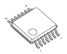
7. 封装信息: - 提供了DIP14、SOP14、SOL14和TSSOP14四种封装方式,每种封装都有对应的尺寸和重量信息。例如,DIP14的重量为0.96克(典型值)。
TC74AC14FT 价格&库存

很抱歉,暂时无法提供与“TC74AC14FT”相匹配的价格&库存,您可以联系我们找货

免费人工找货