TOSHIBA CCD Linear Image Sensor
CCD (Charge Coupled Device)
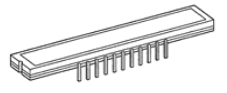
TCD1209DG
�TCD1209DG
TOSHIBA CCD Linear Image Sensor
CCD (Charge Coupled Device)
TCD1209DG
The TCD1209DG is a high sensitive and low dark current 2048
elements CCD linear image sensor.
The device contains a row of 2048 elements photodiodes which
provide 8 lines/mm across a B4 size paper. The device is operated
by 5.0 V pulse and 12 V power supply.
Features
Number of Image Sensing Elements: 2048 elements
Image Sensing Element Size: 14μm by 14μm on 14μm center
Photo Sensing Region: High sensitive PN photodiode
Clock: 2-phase (5 V)
Power Supply Voltage: 12 V (typ.)
Package: 22 pin CERDIP
WDIP22-G-400-2.54H
ABSOLUTE MAXIMUM RATINGS (Note 1)
Characteristic
Symbol
Pin Connections (top view)
Rating
Unit
−0.3 to +8.0
V
Clock pulse voltage
V
Shift pulse voltage
VSH
Reset pulse voltage
VRS
Clamp pulse voltage
VCP
Power supply voltage
VOD
-0.3 to +15.0
V
Operating temperature
Topr
−25 to +60
°C
Storage temperature
Tstg
−40 to +100
°C
Note 1: All voltages are with respect to SS terminals (ground).
None of the ABSOLUTE MAXIMUM RATINGS must be exceeded,
even instantaneously.
If any one of the ABSOLUTE MAXIMUM RATINGS is exceeded,
the electrical characteristics, reliability and life time of the device
cannot be guaranteed. If the ABSOLUTE MAXIMUM RATINGS are
exceeded, the device can be permanently damaged or degraded.
Create a system design in such a manner that any of the
ABSOLUTE MAXIMUM RATINGS will not be exceeded under any
circumstances.
© 2018
Toshiba Electronic Devices & Storage Corporation
1
Rev.2.2 2019-01-08
�TCD1209DG
Circuit Diagram
Photodiode
Pin Names
Pin No.
Symbol
1
OS
2
SS
3
Name
Pin No.
Symbol
Output signal
22
SH
Shift gate
Ground
21
CP
Clamp gate
OD
Power supply
20
NC
Non connection
4
NC
Non connection
19
NC
Non connection
5
1
Transfer clock (phase 1)
18
RS
Reset gate
6
2
Transfer clock (phase 2)
17
2B
Last stage transfer clock (phase 2)
7
NC
Non connection
16
NC
Non connection
8
NC
Non connection
15
NC
Non connection
9
NC
Non connection
14
NC
Non connection
10
NC
Non connection
13
NC
Non connection
11
NC
Non connection
12
NC
Non connection
© 2018
Toshiba Electronic Devices & Storage Corporation
2
Name
Rev.2.2 2019-01-08
�TCD1209DG
Optical/Electrical Characteristics
Ta 25°C, VOD 12 V, V VSH VRS VCP 5 V (pulse), f 1.0 MHz,
tINT (integration time) 10 ms, light source daylight fluorescent lamp
Characteristic
Symbol
Min
Typ.
Max
Unit
Note
R
25
31
37
V/lxs
―
PRNU (1)
―
3
10
%
(Note 2)
PRNU (3)
―
4
10
mV
(Note 8)
Sensitivity
Photo response non uniformity
VSAT
1.5
2.0
―
V
(Note 3)
Saturation exposure
SE
0.04
0.06
―
lxs
(Note 4)
Dark signal voltage
VDRK
―
1.0
2.5
mV
(Note 5)
Dark signal non uniformity
DSNU
―
1.0
2.5
mV
(Note 5)
DC power dissipation
PD
―
160
400
mW
―
Total transfer efficiency
TTE
92
98
―
%
―
Output impedance
ZO
―
0.2
1.0
kΩ
―
Dynamic range
DR
―
2000
―
―
(Note 6)
DC output signal voltage
VOS
4.0
5.5
7.0
V
(Note 7)
Random noise
NDσ
―
0.6
―
mV
(Note 9)
Saturation output voltage
Note 2: PRNU (1) is defined on a single chip by the expressions below when the photosensitive surface is applied
with the light of uniform illumination and uniform color temperature, where measured approximately 500 mV
of signal output.
PRNU(1)
X
X
100 (%)
X : Average of total signal outputs
X: The maximum deviation from X
Note 3: VSAT is defined as the minimum saturation output voltage of all effective pixels.
Note 4: Definition of SE:
VSAT
SE
R
Note 5: VDRK is defined as average dark signal voltage of all effective pixels.
DSNU is defined by the difference between average value (VDRK) and the maximum value of the dark
voltage.
OS
VDRK
DSNU
Note 6: Definition of DR:
VSAT
DR
VDRK
VDRK is proportional to tINT (integration time). So the shorter integration time makes wider dynamic range.
© 2018
Toshiba Electronic Devices & Storage Corporation
3
Rev.2.2 2019-01-08
�TCD1209DG
Note 7: DC output signal voltage is defined as follows.
OS
VOS
SS
Note 8: PRNU (3) is defined as the maximum voltage with next pixel, where measured approximately 50 mV of signal
output.
Note 9: Random noise is defined as the standard deviation (sigma) of the output level difference between two
adjacent effective pixels under no illumination (i.e. dark condition) calculated by the following procedure.
Video output
period
Video output
period
200 ns
200 ns
Output waveform
(effective pixels under dark condition)
V
Pixel n+1
Pixel n
1)
2)
3)
4)
Two adjacent pixels (pixel n and n1) in one reading are fixed as measurement points.
Each of the output levels at video output periods averaged over 200 ns period to get V(n) and V(n1).
V(n1) is subtracted from V(n) to get V.
V V(n) V(n1)
The standard deviation of V is calculated after procedure 2) and 3) are repeated 30 times (30 readings).
ΔV
5)
6)
1 30
2
| Vi| V
30 i 1
Procedure 2), 3) and 4) are repeated 10 times to get sigma value.
10 sigma values are averaged.
7)
1 30
ΔVi
30 i1
1 10
j
10 j1
value calculated using the above procedure is observed
2 times larger than that measured relative
to the ground level. So we specify the random noise as follows.
ND
1
2
© 2018
Toshiba Electronic Devices & Storage Corporation
4
Rev.2.2 2019-01-08
�TCD1209DG
Recommended Operating Conditions (Ta 25°C)
For best performance, the device should be used within the Recommended Operating Conditions.
Characteristics
Clock pulse voltage
Symbol
Min
Typ.
Max
“H” level
V1
4.5
5.0
5.5
“L” level
V2
0
0
0.5
4.5
5.0
5.5
0
0
0.5
4.5
5.0
5.5
0
0
0.5
4.5
5.0
5.5
0
0
0.5
4.5
5.0
5.5
0
0
0.5
11.4
12.0
13.0
“H” level
Last stage clock pulse voltage
V2B
“L” level
“H” level
Shift pulse voltage
VSH
“L” level
“H” level
Reset pulse voltage
VRS
“L” level
“H” level
Clamp pulse voltage
VCP
“L” level
Power supply voltage
VOD
Unit
V
V
V
V
V
V
Clock Characteristics (Ta 25°C)
For best performance, the device should be used within the Recommended Operating Conditions.
Characteristic
Symbol
Min
Typ.
Max
Unit
Clock pulse frequency
f
1
20
MHz
Reset pulse frequency
fRS
1
20
MHz
C1
200
pF
Clock capacitance
(Note 10)
C2
200
pF
Last stage clock capacitance
C2B
10
20
pF
Shift gate capacitance
CSH
30
pF
Reset gate capacitance
CRS
10
20
pF
Clamp gate capacitance
CCP
10
20
pF
Note 10: VOD 12 V
© 2018
Toshiba Electronic Devices & Storage Corporation
5
Rev.2.2 2019-01-08
�TCD1209DG
Timing Chart
*1: Keep the RS pin “L” level.
*2: Keep the CP pin “L” level.
© 2018
Toshiba Electronic Devices & Storage Corporation
6
Rev.2.2 2019-01-08
�TCD1209DG
Timing Requirements
2B, RS, CP Timing
SH,1 Timing
t2
t4
t3
4.5 V
2B
SH
0.5 V
4.5 V 4.5 V
t6
0.5 V
0.5 V
0.5 V
t7
t9
t15
0.5 V
t1
1
4.5 V
t5
4.5 V
RS
4.5 V
4.5 V
0.5 V
4.5 V
0.5 V
t8
CP
t10
t13
4.5 V
t16
4.5 V
0.5 V
0.5 V
t12
t14
t11
OS
0.5 V
SH,RS,CP Timing
SH
0.5 V
0.5 V
t18
t19
4.5 V
RS
0. 5V
0.5 V
t17
t16
(Note 11)
4.5 V
CP
0.5 V
0.5 V
Note 11: Keep the RS and CP pins “L” level.
1, 2 Cross point
1
t20
t20
4.0 V
(min)
4.0 V
(min)
1.5 V (min)
1.5 V (min)
2
SS
© 2018
Toshiba Electronic Devices & Storage Corporation
7
Rev.2.2 2019-01-08
�TCD1209DG
Symbol
Min
Typ.
(Note 12)
Max
Unit
Pulse timing of SH and 1
t1, t5
200
+t8+t12+t13+t14
+t16
500
ns
SH pulse rise time, fall time
t2, t4
0
50
ns
t3
1000
1500
ns
2B pulse rise time, fall time
t6, t7
0
100
ns
RS pulse rise time, fall time
t8, t10
0
20
ns
RS pulse width
t9
10
100
ns
Video data delay time
t11
15
ns
t12, t14
0
20
ns
CP pulse width
t13
10
100
ns
Pulse timing of2B and CP
t15
0
50
ns
t16
0
100
ns
t17
10
100
ns
Pulse timing of SH and CP
t18
200
ns
Pulse timing of SH and RS
t19
200
ns
Pulse timing of 1 and 2
t20
17
ns
Characteristic
SH pulse width
CP pulse rise time, fall time
Pulse timing of RS and CP
Note 12: Measured with f 1 MHz.
© 2018
Toshiba Electronic Devices & Storage Corporation
8
Rev.2.2 2019-01-08
�TCD1209DG
Cautions
1.
Electrostatic Breakdown
Store in shorting clip or in conductive foam to avoid electrostatic breakdown.
CCD Image Sensor is protected against static electricity, but inferior puncture mode device due to static
electricity is sometimes detected. In handing the device, it is necessary to execute the following static electricity
preventive measures, in order to prevent the trouble rate increase of the manufacturing system due to static
electricity.
a.
b.
c.
d.
Prevent the generation of static electricity due to friction by making the work with bare hands or by putting
on cotton gloves and non-charging working clothes.
Discharge the static electricity by providing earth plate or earth wire on the floor, door or stand of the work
room.
Ground the tools such as soldering iron, radio cutting pliers of or pincer.
Ionized air is recommended for discharge when handling CCD image sensors.
It is not necessarily required to execute all precaution items for static electricity.
It is all right to mitigate the precautions by confirming that the trouble rate within the prescribed range.
2.
Window Glass
The dust and stain on the glass window of the package degrade optical performance of CCD sensor.
Keep the glass window clean by saturating a cotton swab in alcohol and lightly wiping the surface, and allow the
glass to dry, by blowing with filtered dry N2. Care should be taken to avoid mechanical or thermal shock because
the glass window is easily to damage.
3.
Incident Light
CCD sensor is sensitive to infrared light. Note that infrared light component degrades resolution and PRNU of
CCD sensor.
4.
Mounting on a PCB
This package is sensitive to mechanical stress.
TOSHIBA recommends using IC inserters for mounting, instead of using lead forming equipment.
Since this package is not strong against mechanical stress, you should not reform the lead frame.
We recommend to use an IC-inserter when you assemble to PCB.
5.
Soldering
Soldering by the solder flow method cannot be guaranteed because this method may have deleterious effects
on prevention of window glass soiling and heat resistance.
Using a soldering iron, complete soldering within three seconds for lead temperatures of up to 350°C.
© 2018
Toshiba Electronic Devices & Storage Corporation
9
Rev.2.2 2019-01-08
�TCD1209DG
Package Dimensions
WDIP22-G-400-2.54H
Unit: mm
Note 1: Distance between the edge of the package and the first pixel (S1)
Note 2: Distance between the top of chip and bottom of the package
Note 3: Glass thickness (n = 1.5)
© 2018
Toshiba Electronic Devices & Storage Corporation
10
Rev.2.2 2019-01-08
�TCD1209DG
RESTRICTIONS ON PRODUCT USE
Toshiba Corporation and its subsidiaries and affiliates are collectively referred to as “TOSHIBA”.
Hardware, software and systems described in this document are collectively referred to as “Product”.
TOSHIBA reserves the right to make changes to the information in this document and related Product without notice.
This document and any information herein may not be reproduced without prior written permission from TOSHIBA. Even with
TOSHIBA's written permission, reproduction is permissible only if reproduction is without alteration/omission.
Though TOSHIBA works continually to improve Product's quality and reliability, Product can malfunction or fail. Customers are
responsible for complying with safety standards and for providing adequate designs and safeguards for their hardware, software and
systems which minimize risk and avoid situations in which a malfunction or failure of Product could cause loss of human life, bodily
injury or damage to property, including data loss or corruption. Before customers use the Product, create designs including the
Product, or incorporate the Product into their own applications, customers must also refer to and comply with (a) the latest versions of
all relevant TOSHIBA information, including without limitation, this document, the specifications, the data sheets and application
notes for Product and the precautions and conditions set forth in the "TOSHIBA Semiconductor Reliability Handbook" and (b) the
instructions for the application with which the Product will be used with or for. Customers are solely responsible for all aspects of their
own product design or applications, including but not limited to (a) determining the appropriateness of the use of this Product in such
design or applications; (b) evaluating and determining the applicability of any information contained in this document, or in charts,
diagrams, programs, algorithms, sample application circuits, or any other referenced documents; and (c) validating all operating
parameters for such designs and applications. TOSHIBA ASSUMES NO LIABILITY FOR CUSTOMERS' PRODUCT DESIGN OR
APPLICATIONS.
PRODUCT IS NEITHER INTENDED NOR WARRANTED FOR USE IN EQUIPMENTS OR SYSTEMS THAT REQUIRE
EXTRAORDINARILY HIGH LEVELS OF QUALITY AND/OR RELIABILITY, AND/OR A MALFUNCTION OR FAILURE OF WHICH
MAY CAUSE LOSS OF HUMAN LIFE, BODILY INJURY, SERIOUS PROPERTY DAMAGE AND/OR SERIOUS PUBLIC IMPACT
("UNINTENDED USE"). Except for specific applications as expressly stated in this document, Unintended Use includes, without
limitation, equipment used in nuclear facilities, equipment used in the aerospace industry, lifesaving and/or life supporting medical
equipment, equipment used for automobiles, trains, ships and other transportation, traffic signaling equipment, equipment used to
control combustions or explosions, safety devices, elevators and escalators, and devices related to power plant. IF YOU USE
PRODUCT FOR UNINTENDED USE, TOSHIBA ASSUMES NO LIABILITY FOR PRODUCT. For details, please contact your
TOSHIBA sales representative or contact us via our website.
Do not disassemble, analyze, reverse-engineer, alter, modify, translate or copy Product, whether in whole or in part.
Product shall not be used for or incorporated into any products or systems whose manufacture, use, or sale is prohibited under any
applicable laws or regulations.
The information contained herein is presented only as guidance for Product use. No responsibility is assumed by TOSHIBA for any
infringement of patents or any other intellectual property rights of third parties that may result from the use of Product. No license to
any intellectual property right is granted by this document, whether express or implied, by estoppel or otherwise.
ABSENT A WRITTEN SIGNED AGREEMENT, EXCEPT AS PROVIDED IN THE RELEVANT TERMS AND CONDITIONS OF
SALE FOR PRODUCT, AND TO THE MAXIMUM EXTENT ALLOWABLE BY LAW, TOSHIBA (1) ASSUMES NO LIABILITY
WHATSOEVER, INCLUDING WITHOUT LIMITATION, INDIRECT, CONSEQUENTIAL, SPECIAL, OR INCIDENTAL DAMAGES
OR LOSS, INCLUDING WITHOUT LIMITATION, LOSS OF PROFITS, LOSS OF OPPORTUNITIES, BUSINESS INTERRUPTION
AND LOSS OF DATA, AND (2) DISCLAIMS ANY AND ALL EXPRESS OR IMPLIED WARRANTIES AND CONDITIONS RELATED
TO SALE, USE OF PRODUCT, OR INFORMATION, INCLUDING WARRANTIES OR CONDITIONS OF MERCHANTABILITY,
FITNESS FOR A PARTICULAR PURPOSE, ACCURACY OF INFORMATION, OR NONINFRINGEMENT.
Do not use or otherwise make available Product or related software or technology for any military purposes, including without
limitation, for the design, development, use, stockpiling or manufacturing of nuclear, chemical, or biological weapons or missile
technology products (mass destruction weapons). Product and related software and technology may be controlled under the
applicable export laws and regulations including, without limitation, the Japanese Foreign Exchange and Foreign Trade Law and the
U.S. Export Administration Regulations. Export and re-export of Product or related software or technology are strictly prohibited
except in compliance with all applicable export laws and regulations.
Please contact your TOSHIBA sales representative for details as to environmental matters such as the RoHS compatibility of Product.
Please use Product in compliance with all applicable laws and regulations that regulate the inclusion or use of controlled substances,
including without limitation, the EU RoHS Directive. TOSHIBA ASSUMES NO LIABILITY FOR DAMAGES OR LOSSES
OCCURRING AS A RESULT OF NONCOMPLIANCE WITH APPLICABLE LAWS AND REGULATIONS.
https://toshiba.semicon-storage.com/
© 2018
Toshiba Electronic Devices & Storage Corporation
11
Rev.2.2 2019-01-08
�


 工商网监
湘ICP备2023018690号
工商网监
湘ICP备2023018690号

