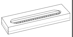
TOSHIBA CCD Linear Image Sensor
CCD (Charge Coupled Device)
TCD1254GFG
�TCD1254GFG
TOSHIBA CCD Linear Image Sensor
CCD (Charge Coupled Device)
TCD1254GFG
The TCD1254GFG is a high sensitive and low dark current 2500
elements CCD linear image sensor.
This device consists of sensitivity CCD chip.
The TCD1254GFG has electronic shutter function (ICG).
Electronic shutter function can keep always output voltage constant
that vary with intensity of lights.
Features
WQFN16X-240A
Number of Image Sensing Elements: 2500 elements
Image Sensing Element Size: 5.25m by 64m on 5.25 m
Photo Sensing Region: High sensitive PN photodiode
Power Supply Voltage: 3.0 V (min)
Internal Circuit: CCD drive circuit
Package: 16 pin GLCC
Function: Electronic shutter, Sample and hold circuit
center
ABSOLUTE MAXIMUM RATINGS (Note 1)
Characteristic
Symbol
Pin Connections (top view)
Rating
Unit
-0.3 to +7.0
V
Information in this datasheet is preliminary and should not be relied on in undertaking system design.
Master clock pulse voltage
VM
Shift pulse voltage
VSH
Integration clear pulse voltage
VICG
Digital power supply voltage
VDD
Analog power supply voltage
VAD
Operating temperature
Topr
-25 to +60
°C
Storage temperature
Tstg
-40 to +85
°C
Note 1: All voltages are with respect to SS terminals (ground).
None of the ABSOLUTE MAXIMUM RATINGS must be exceeded,
even instantaneously.
If any one of the ABSOLUTE MAXIMUM RATINGS is exceeded,
the electrical characteristics, reliability and life time of the device
cannot be guaranteed. If the ABSOLUTE MAXIMUM RATINGS are
exceeded, the device can be permanently damaged or degraded.
Create a system design in such a manner that any of the
ABSOLUTE MAXIMUM RATINGS will not be exceeded under any
circumstances.
© 2017
Toshiba Electronic Devices & Storage Corporation
1
Rev.1.3 2019-01-24
�TCD1254GFG
Circuit Diagram
CCD analog shift register 2
Shift gate 2
Integration clear gate 2
Signal
output
buffer
Photodiode
Integration clear gate 1
Shift gate 1
CCD analog shift register 1
Logic circuit
Pin Names
Information in this datasheet is preliminary and should not be relied on in undertaking system design.
Pin No.
Symbol
1
OS
2
SS
3
4
Name
Pin No.
Symbol
Name
Output signal
16
NC
Non connection*
Ground
15
NC
Non connection*
VAD
Power supply (Analog)
14
NC
Non connection*
VDD
Power supply (Digital)
13
NC
Non connection*
5
M
Master clock
12
NC
Non connection*
6
ICG
Integration clear gate
11
NC
Non connection*
7
SH
Shift gate
10
NC
Non connection*
8
NC
Non connection*
9
NC
Non connection*
* All NC pins should be kept open, or connected to ground on PCB.
© 2017
Toshiba Electronic Devices & Storage Corporation
2
Rev.1.3 2019-01-24
�TCD1254GFG
Optical/Electrical Characteristics
Ta 25°C, VAD VDD 4.0 V, V 4.0 V (pulse), fM 2.0 MHz (data rate 1.0 MHz),
tINT (integration time) 10 ms, light source daylight fluorescent lamp
Characteristics
Sensitivity
Photo response non uniformity
Register imbalance
Symbol
Min
Typ.
Max
Unit
Note
R
72
103
V/lxs
(Note 2)
PRNU
10
%
(Note 3)
RI
1.5
3
%
(Note 4)
VSAT
0.7
1.0
V
(Note 5)
Saturation exposure
SE
0.01
lxs
(Note 6)
Dark signal voltage
VMDK
2.5
15
mV
(Note 7)
DC power dissipation
PD
24
60
mW
Total transfer efficiency
TTE
92
95
%
(Note 8)
92
95
%
(Note 9)
83
88
%
(Note 10)
ZO
0.5
1.0
k
DC output signal voltage
VOS
1.5
2.3
3.0
V
(Note 11)
Dynamic range
DR
400
(Note 12)
Saturation output voltage
Low voltage total transfer efficiency
Output impedance
LVTTE
Note 2: Sensitivity is defined for signal outputs average when the photosensitive surface is applied with the light of
uniform illumination and uniform color temperature.
Note 3: PRNU is defined for a single chip by the expressions below when the photosensitive surface is applied with
the light of uniform illumination and uniform color temperature, where measured approximately 500 mV of
signal output.
X
PRNU
100 (%)
X
Information in this datasheet is preliminary and should not be relied on in undertaking system design.
X : Average of total signal outputs
X: The maximum deviation from X
Note 4: Register imbalance is defined as follows.
Y
×100 (%)
RI
X
X : Average of total signal outputs
Y: | average of odd effective signal outputs average of even effective signal outputs |
Note 5: VSAT is defined as the minimum saturation output voltage of all effective pixels.
Note 6: Definition of SE:
VSAT
SE
R
Note 7: VMDK is defined as the maximum dark signal voltage of all effective pixels.
OS
VMDK
© 2017
Toshiba Electronic Devices & Storage Corporation
3
Rev.1.3 2019-01-24
�TCD1254GFG
Note 8: Total transfer efficiency is defined as follows.
* Q0 500 mV
Average of dummy outputs
Q1’
Q0’
Q0
Q1
TTE
Q0
100
Q0 Q1
Use Q0’ and Q1’ instead of Q0 and Q1 if Q1’ Q1.
Note 9: Definition of low voltage total transfer efficiency is the same as Note 8 without power supply and Q0.
* 4 V Power supply 5 V
* Q0 50 mV
Note 10: Definition is the same as Note 9 without power supply as follows.
* 3 V Power supply 4 V
Note 11: DC output signal voltage is defined as follows.
OS
VOS
SS
Information in this datasheet is preliminary and should not be relied on in undertaking system design.
Note 12: Definition of DR:
VSAT
DR
VMDK
VMDK is proportional to tINT (integration time). So the shorter integration time makes wider dynamic range.
© 2017
Toshiba Electronic Devices & Storage Corporation
4
Rev.1.3 2019-01-24
�TCD1254GFG
Recommended Operating Conditions (Ta 25°C)
For best performance, the device should be used within the Recommended Operating Conditions.
Characteristics
Symbol
“H” level
Master clock pulse voltage
VM
“L” level
“H” level
Shift pulse voltage
VSH
“L” level
“H” level
Integration clear pulse voltage
VICG
“L” level
Min
Typ.
Max
3.0
4.0
5.0
0
0
0.44
3.0
4.0
5.0
0
0
0.44
3.0
4.0
5.0
0
0
0.44
Unit
Note
V
(Note 13)
V
(Note 13)
V
(Note 13)
Power supply voltage (Digital)
VDD
3.0
4.0
5.0
V
(Note 14)
Power supply voltage (Analog)
VAD
3.0
4.0
5.0
V
(Note 14)
Note 13: “H” level of the maximum pulse voltage VDD VDD 0.5 V “H” level of the minimum pulse voltage.
Note 14: VAD VDD
Clock Characteristics (Ta 25°C) (3.0 V VAD VDD 5.0 V)
For best performance, the device should be used within the Recommended Operating Conditions.
Characteristics
Symbol
Min
Typ.
Max
Unit
fM
0.4
2.0
4.0
MHz
fDATA
0.2
1.0
2.0
MHz
10
pF
Master clock pulse frequency
Data rate
Master clock capacitance
CM
Shift gate capacitance
CSH
200
pF
Integration clear gate capacitance
CICG
50
pF
Information in this datasheet is preliminary and should not be relied on in undertaking system design.
Power-on Characteristics
CCD sensor has the characteristics that a correct output signal will be appeared after power supply reached to regular
voltage. It is required to 10 cycles of read out time at least after power supply reached to regular voltage. This
characteristics should be considered, when circuit designs.
© 2017
Toshiba Electronic Devices & Storage Corporation
5
Rev.1.3 2019-01-24
�TCD1254GFG
Timing Chart 1
tINT(integration time)
SH
ICG
M
Dummy outputs
(16 elements)
D45
D46
D44
D43
D41
D42
S2498
S2499
S2500
D32
D33
D34
D35
D36
D37
S2496
S2497
D25
D26
D27
D28
D29
D30
D31
S1
S2
S3
D13
D14
D15
D16
D17
D18
D19
OS
D0
D1
D2
D3
Information in this datasheet is preliminary and should not be relied on in undertaking system design.
Light shielded outputs
(13 elements)
(3 elements)
Dummy outputs (32 elements)
Effective outputs
(2500 elements)
Dummy outputs (15 elements)
1 line readout period (2547 elements)
© 2017
Toshiba Electronic Devices & Storage Corporation
6
Rev.1.3 2019-01-24
�TCD1254GFG
Timing Chart 2 (Use Electronic Shutter Function)
tINT (integration time)
Readout time
SH
ICG
M
Dummy outputs
(16 elements)
D45
D46
D44
D43
D41
D42
S2498
S2499
S2500
D32
D33
D34
D35
D36
D37
S2496
S2497
D25
D26
D27
D28
D29
D30
D31
S1
S2
S3
D13
D14
D15
D16
D17
D18
D19
OS
D0
D1
D2
D3
Information in this datasheet is preliminary and should not be relied on in undertaking system design.
Light shielded outputs
(13 elements)
(3 elements)
Dummy outputs (32 elements)
Effective outputs
(2500 elements)
Dummy outputs (15 elements)
1 line readout period (2547 elements)
© 2017
Toshiba Electronic Devices & Storage Corporation
7
Rev.1.3 2019-01-24
�TCD1254GFG
Timing Requirements
t2
t3
t1
t4
SH
ICG
M
OS
Characteristics
D1
D0
D2
Symbol
Min
Typ.
Max
Unit
ICG pulse delay
t1
1000
5000
ns
Pulse timing of ICG and SH
t2
100
500
1000
ns
Shift pulse width
t3
1000
ns
Pulse timing of ICG and M
t4
0
20
ns
*: To keep M “H” level when ICG switch from “L” to “H” level.
Information in this datasheet is preliminary and should not be relied on in undertaking system design.
Use Electronic Shutter
Pulse timing of SH and ICG
tINT (integration time)
t3 **
***
***
***
****
・・・・・・・・・・・
SH
ICG
Readout time
** : Each SH high pulse have to keep always the same value with “t3“. (t3 1000 ns (min))
*** : SH pulse cycle have to keep the same cycle (SH cycle period 10 s) except tINT period.
**** : tINT 10 s (min)
Note:
The illumination of light source must be used with less than 1000 times based on 0.7 V signal output with10
ms tINT.
© 2017
Toshiba Electronic Devices & Storage Corporation
8
Rev.1.3 2019-01-24
�TCD1254GFG
Typical Performance Curves
Relative response
Spectral Response
Wavelength [nm]
Sensitivity Response
SENSITIVITY
RESPONSE
200
Sensitivity [V/lx·s]
SENSITIVITY
(V/lx.s)
Information in this datasheet is preliminary and should not be relied on in undertaking system design.
150
100
50
0
3
3.5
4
4.5
5
PowerSUPPLY
supply VAD
, VDDVDD
[V] (V)
POWER
VAD,
© 2017
Toshiba Electronic Devices & Storage Corporation
9
Rev.1.3 2019-01-24
�TCD1254GFG
Typical Performance Curves
DC output signal voltage VOS [V]
DC Output Signal Voltage –
Power Supply Voltage
Power supply VAD, VDD [V]
Information in this datasheet is preliminary and should not be relied on in undertaking system design.
© 2017
Toshiba Electronic Devices & Storage Corporation
10
Rev.1.3 2019-01-24
�TCD1254GFG
Typical Drive Circuit
* All NC pins should be kept open, or connected to ground on PCB.
4.0 V
4.0 V
10 F/25 V
Information in this datasheet is preliminary and should not be relied on in undertaking system design.
© 2017
Toshiba Electronic Devices & Storage Corporation
11
Rev.1.3 2019-01-24
�TCD1254GFG
Cautions
1.
Electrostatic Breakdown
Store in shorting clip or in conductive foam to avoid electrostatic breakdown.
CCD Image Sensor is protected against static electricity, but inferior puncture mode device due to static electricity
is sometimes detected. In handing the device, it is necessary to execute the following static electricity preventive
measures, in order to prevent the trouble rate increase of the manufacturing system due to static electricity.
a.
b.
c.
d.
e.
Prevent the generation of static electricity due to friction by making the work with bare hands or by putting
on cotton gloves and non-charging working clothes.
Discharge the static electricity by providing earth plate or earth wire on the floor, door or stand of the work
room.
Ground the tools such as cutting pliers, tweezers or pincer.
When the product is handed, please use tweezers to avoid the damage of CCD image sensor.
Ionized air is recommended for discharge when handling CCD image sensors.
It is not necessarily required to execute all precaution items for static electricity.
It is all right to mitigate the precautions by confirming that the trouble rate within the prescribed range.
2.
Incident Light
CCD sensor is sensitive to infrared light. Note that infrared light component degrades resolution and PRNU of
CCD sensor.
3.
Ultrasonic Cleaning
Ultrasonic cleaning should not be used with such hermetically-sealed ceramic package as CCD because the
bonding wires can become disconnected due to resonance during the cleaning process.
4.
Window Glass
The dust and stain on the glass window of the package degrade optical performance of CCD sensor.
Keep the glass window clean by saturating a cotton swab in alcohol and lightly wiping the surface, and allow the
glass to dry, by blowing with filtered dry N2. Care should be taken to avoid mechanical or thermal shock because
the glass window is easily to damage.
Information in this datasheet is preliminary and should not be relied on in undertaking system design.
© 2017
Toshiba Electronic Devices & Storage Corporation
12
Rev.1.3 2019-01-24
�TCD1254GFG
5.
Cleaning Method of the Window Glass Surface
Wiping Cloth
a.
Use soft cloth with a fine mesh.
b.
The wiping cloth must not cause dust from itself.
c.
Use a clean wiping cloth necessarily.
Cleaner
When using solvents, such as alcohol, unavoidably, it is cautious of the next.
a.
A clean thing with quick-drying.
b.
After liquid dries, there needs to be no residual substance.
c.
A thing safe for a human body.
And, please observe the use term of a solvent and use the storage container of a solvent to be clean.
Be cautious of fire enough.
Way of Cleaning
First, the surface of window glass is wiped with the wiping cloth into which the cleaner was infiltrated. Please wipe
down the surface of window glass at least 2 times or more.
Next, the surface of window glass wipes with the dry wiping cloth. Please wipe down the surface of window glass
at least 3 times or more.
Finally, blow cleaning is performed by dry N2 filtered.
If operator wipes the surface of the window glass with the above-mentioned process and dirt still remains,
TOSHIBA recommends repeating the clean operation from the beginning.
Be cautious of the next thing.
a.
Don't infiltrate the cleaner too much.
b.
A wiping portion is performed into the optical range and don't touch the edge of window glass.
c.
Be sure to wipe in a long direction and the same direction.
d.
A wiping cloth always uses an unused portion.
Information in this datasheet is preliminary and should not be relied on in undertaking system design.
Wiper
© 2017
Toshiba Electronic Devices & Storage Corporation
13
Rev.1.3 2019-01-24
�TCD1254GFG
The Standard Reflow Condition for GLCC (Surface Mount Device)
1.
Storage Precautions
1)
2)
3)
4)
5)
6)
2.
CCD surface mount products may have a haze on the inside of glass, so be careful about following. Even if
the haze arises inside of glass, when it is not on the pixel area, there is no problem in quality.
Do not drop or toss device packaging. The laminated aluminum material in it can be rendered ineffective by
rough handling.
Ensure devices should be stored in a 30°C·90 %RH or better environment. Use devices within 12 months;
do not store them longer than that.
In the following cases, in order to remove humidity from a device, bake for 24 hours at 125°C. When a
"30 % humidity indicator" has become pink after the package opened, or when the effective period of the
indicator has passed.
Prevent destruction of the device by static electricity in the case of the bake processing for removing
humidity.
After opening moisture-proof packing, store a product in 30°C·60 %RH or better environment and use them
within five days. If the effective usage period passed after opening the moisture-proof packing, baking
should be done before use at 125°C for 24 hours.
Mounting Conditions Using Reflow
1)
Mounting method:
2)
3)
Preheating condition:
Reflow condition:
4)
Heating times:
(a) Hot air reflow
(b) Infrared ray reflow
150 to 180°C, 60 to 120 s
(a) Maximum 240°C
(b) Over 230°C, within 30 to 50 s
Only 1 time
* The temperature profile is specified in terms of the temperature of top surface of the device.
This temperature profile shows the maximum guaranteed device temperature. Please set up the
optimum temperature profile conditions within the fig.1 profile.
Information in this datasheet is preliminary and should not be relied on in undertaking system design.
Reflow Profile
Main-Heat
30 to 50 [s]
Pre-Heat
60 to 120 [s]
Time [s]
fig.1 Example of recommended temperature profile for reflows
In addition, in case of the repair work accompanied by IC removal, since the degree of parallel may be spoiled
with the left solder, please do not carry out.
© 2017
Toshiba Electronic Devices & Storage Corporation
14
Rev.1.3 2019-01-24
�TCD1254GFG
3.
Mounting
1)
2)
3)
4)
5)
4.
In the case of solder mounting, the devices should be mounted with the window glass protective tape in
order to avoid dust or dirt included in reflow machine.
The window glass protective tape is manufactured from materials in which static charges tend to build up.
When removing the tape from CCD sensor after solder mounting, install an ionizer to prevent the tape from
being charged with static electricity.
When the tape is removed, adhesives will remain in the glass surface. Since these adhesives appear as
black or white flaws on the image, please wipe the window glass surface with the cloth into which the
organic solvent was infiltrated. Then please attach CCD to a product.
Do not reuse the window glass protective tape.
The parts of glass seal area have possibility to be became clouded by reflow process, however, there is no
problem in quality.
Foot Pattern on the PCB
We recommend fig.2’s foot pattern for your PCB (Printed Circuit Board).
Unit: mm
Information in this datasheet is preliminary and should not be relied on in undertaking system design.
fig.2 Foot pattern
5.
Mask for Solder Paste Application
We recommend metal mask that have the following thickness.
Thickness: 0.1 mm.
And we recommend that the opened area size on the metal mask is 100 % for pads on solder.
© 2017
Toshiba Electronic Devices & Storage Corporation
15
Rev.1.3 2019-01-24
�TCD1254GFG
Package Dimensions
WQFN16X-240A
3.250.15
Unit: mm
13.13(5.25 µm 2500)
Information in this datasheet is preliminary and should not be relied on in undertaking system design.
Note 1: Distance between the edge of the package and the first pixel (S1)
Note 2: Distance between the top of chip and bottom of the package
Note 3: Distance between the edge of the package and the chip center
© 2017
Toshiba Electronic Devices & Storage Corporation
16
Rev.1.3 2019-01-24
�TCD1254GFG
RESTRICTIONS ON PRODUCT USE
Toshiba Corporation and its subsidiaries and affiliates are collectively referred to as “TOSHIBA”.
Hardware, software and systems described in this document are collectively referred to as “Product”.
TOSHIBA reserves the right to make changes to the information in this document and related Product without notice.
This document and any information herein may not be reproduced without prior written permission from TOSHIBA. Even with
TOSHIBA's written permission, reproduction is permissible only if reproduction is without alteration/omission.
Though TOSHIBA works continually to improve Product's quality and reliability, Product can malfunction or fail. Customers are
responsible for complying with safety standards and for providing adequate designs and safeguards for their hardware, software and
systems which minimize risk and avoid situations in which a malfunction or failure of Product could cause loss of human life, bodily
injury or damage to property, including data loss or corruption. Before customers use the Product, create designs including the Product,
or incorporate the Product into their own applications, customers must also refer to and comply with (a) the latest versions of all
relevant TOSHIBA information, including without limitation, this document, the specifications, the data sheets and application notes for
Product and the precautions and conditions set forth in the "TOSHIBA Semiconductor Reliability Handbook" and (b) the instructions for
the application with which the Product will be used with or for. Customers are solely responsible for all aspects of their own product
design or applications, including but not limited to (a) determining the appropriateness of the use of this Product in such design or
applications; (b) evaluating and determining the applicability of any information contained in this document, or in charts, diagrams,
programs, algorithms, sample application circuits, or any other referenced documents; and (c) validating all operating parameters for
such designs and applications. TOSHIBA ASSUMES NO LIABILITY FOR CUSTOMERS' PRODUCT DESIGN OR APPLICATIONS.
PRODUCT IS NEITHER INTENDED NOR WARRANTED FOR USE IN EQUIPMENTS OR SYSTEMS THAT REQUIRE
EXTRAORDINARILY HIGH LEVELS OF QUALITY AND/OR RELIABILITY, AND/OR A MALFUNCTION OR FAILURE OF WHICH
MAY CAUSE LOSS OF HUMAN LIFE, BODILY INJURY, SERIOUS PROPERTY DAMAGE AND/OR SERIOUS PUBLIC IMPACT
("UNINTENDED USE"). Except for specific applications as expressly stated in this document, Unintended Use includes, without
limitation, equipment used in nuclear facilities, equipment used in the aerospace industry, lifesaving and/or life supporting medical
equipment, equipment used for automobiles, trains, ships and other transportation, traffic signaling equipment, equipment used to
control combustions or explosions, safety devices, elevators and escalators, and devices related to power plant. IF YOU USE
PRODUCT FOR UNINTENDED USE, TOSHIBA ASSUMES NO LIABILITY FOR PRODUCT. For details, please contact your
TOSHIBA sales representative or contact us via our website.
Do not disassemble, analyze, reverse-engineer, alter, modify, translate or copy Product, whether in whole or in part.
Product shall not be used for or incorporated into any products or systems whose manufacture, use, or sale is prohibited under any
applicable laws or regulations.
The information contained herein is presented only as guidance for Product use. No responsibility is assumed by TOSHIBA for any
infringement of patents or any other intellectual property rights of third parties that may result from the use of Product. No license to
any intellectual property right is granted by this document, whether express or implied, by estoppel or otherwise.
Information in this datasheet is preliminary and should not be relied on in undertaking system design.
ABSENT A WRITTEN SIGNED AGREEMENT, EXCEPT AS PROVIDED IN THE RELEVANT TERMS AND CONDITIONS OF SALE
FOR PRODUCT, AND TO THE MAXIMUM EXTENT ALLOWABLE BY LAW, TOSHIBA (1) ASSUMES NO LIABILITY
WHATSOEVER, INCLUDING WITHOUT LIMITATION, INDIRECT, CONSEQUENTIAL, SPECIAL, OR INCIDENTAL DAMAGES OR
LOSS, INCLUDING WITHOUT LIMITATION, LOSS OF PROFITS, LOSS OF OPPORTUNITIES, BUSINESS INTERRUPTION AND
LOSS OF DATA, AND (2) DISCLAIMS ANY AND ALL EXPRESS OR IMPLIED WARRANTIES AND CONDITIONS RELATED TO
SALE, USE OF PRODUCT, OR INFORMATION, INCLUDING WARRANTIES OR CONDITIONS OF MERCHANTABILITY, FITNESS
FOR A PARTICULAR PURPOSE, ACCURACY OF INFORMATION, OR NONINFRINGEMENT.
Do not use or otherwise make available Product or related software or technology for any military purposes, including without limitation,
for the design, development, use, stockpiling or manufacturing of nuclear, chemical, or biological weapons or missile technology
products (mass destruction weapons). Product and related software and technology may be controlled under the applicable export
laws and regulations including, without limitation, the Japanese Foreign Exchange and Foreign Trade Law and the U.S. Export
Administration Regulations. Export and re-export of Product or related software or technology are strictly prohibited except in
compliance with all applicable export laws and regulations.
Please contact your TOSHIBA sales representative for details as to environmental matters such as the RoHS compatibility of Product.
Please use Product in compliance with all applicable laws and regulations that regulate the inclusion or use of controlled substances,
including without limitation, the EU RoHS Directive. TOSHIBA ASSUMES NO LIABILITY FOR DAMAGES OR LOSSES
OCCURRING AS A RESULT OF NONCOMPLIANCE WITH APPLICABLE LAWS AND REGULATIONS.
https://toshiba.semicon-storage.com/
© 2017
Toshiba Electronic Devices & Storage Corporation
17
Rev.1.3 2019-01-24
�


 工商网监
湘ICP备2023018690号
工商网监
湘ICP备2023018690号

