TCR15AG series
TOSHIBA CMOS Linear Integrated Circuit Silicon Monolithic
TCR15AG series
1.5 A CMOS Ultra Low Dropout, Ultra High ripple rejection ratio Regulator
The TCR15AG series are CMOS single output voltage regulators with an
on/off control input, featuring Ultra low dropout voltage, low inrush current
and fast load transient response.
These voltage regulators are available in fixed output voltage type from
0.65 V to 3.6 V and adjustable output voltage type from 0.60 V to 3.6 V and
capable of driving up to 1.5 A.
Other features include Overcurrent protection, Thermal shutdown, Inrush
current reduction, Under voltage lockout and Auto-discharge.
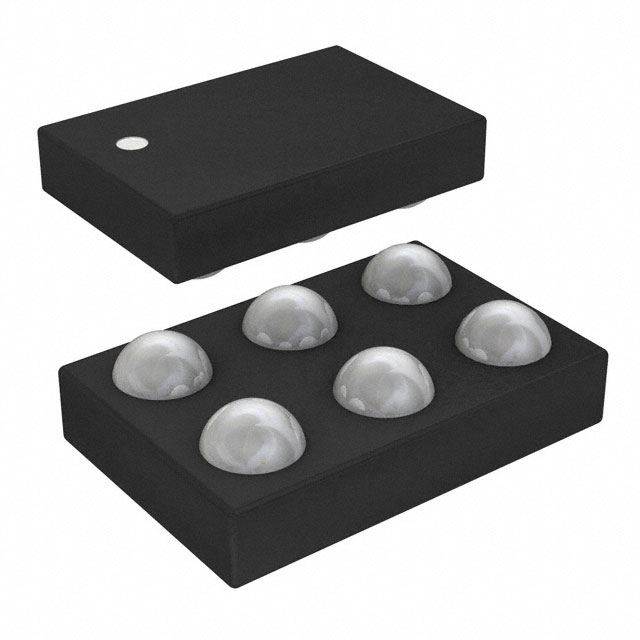
The TCR15AG series are offered in the ultra-small package WCSP6F (0.8
mm x 1.2 mm (typ.), t: 0.33 mm (max))
As small ceramic input and output capacitors can be used with
the TCR15AG series, these device are ideal for portable applications
that require high-density board assembly such as cellular phones.
WCSP6F
Weight : 0.61 mg ( typ.)
Features
•
Low Drop-Out voltage
•
Wide range Output Voltage (Fixed Output Voltage 0.65 V to 3.6 V ,Adjustable Output Voltage 0.6 V to 3.6 V)
•
Fast load transient response
•
High Ripple rejection ratio 95 dB (typ.)@1 kHz
•
Overcurrent protection
-100 / +115 mV (typ.)@ 0.01 A⇔1.5 A, COUT = 4.7 μF
•
Thermal shutdown
•
Auto-discharge
•
Inrush current reduction
•
Output voltage soft start
•
Under voltage lockout
•
Pull down connection between CONTROL and GND
•
Ultra Small package WCSP6F (0.8 mm x 1.2 mm (typ.), t: 0.33 mm (max))
•
Stable with over 4.7 μF Input capacitor, 1.0 μF Bias capacitor and 4.7 μF output ceramic capacitor
Start of commercial production
2017-11
© 2017
Toshiba Electronic Devices & Storage Corporation
1
2017-11-08
�TCR15AG series
Absolute Maximum Ratings (Ta = 25°C)
Characteristics
Symbol
Rating
Unit
Bias voltage
VBIAS
6.0
V
Input voltage
VIN
6.0
V
Control voltage
VCT
-0.3 to VBIAS + 0.3 ≤ 6.0
V
Adjustable voltage
VADJ
-0.3 to 6.0
V
Sense voltage
VSENSE
-0.3 to 6.0
V
Output voltage
VOUT
-0.3 to VIN + 0.3 ≤ 6.0
V
Power dissipation
PD
1.35
W
Junction temperature
Tj
150
°C
Tstg
−55 to 150
°C
Storage temperature range
(Note 1)
Note:
Using continuously under heavy loads (e.g. the application of high temperature/current/voltage and the significant
change in temperature, etc.) may cause this product to decrease in the reliability significantly even if the operating
conditions (i.e. operating temperature/current/voltage, etc.) are within the absolute maximum ratings and the
operating ranges.
Please design the appropriate reliability upon reviewing the Toshiba Semiconductor Reliability Handbook (“Handling
Precautions”/“Derating Concept and Methods”) and individual reliability data (i.e. reliability test report and estimated
failure rate, etc).
Note1:
Rating at mounting on a board
(Glass epoxy board dimension : 40mm x 40mm , 4 layer
Metal pattern ratio : approximately 70% each layer)
Operating Ranges
Characteristics
Bias voltage
Symbol
VBIAS
Rating
VOUT ≤ 1.1 V, IOUT = 1 mA
VOUT > 1.1 V, IOUT = 1 mA
Unit
2.5 to 5.5
V
VOUT + 1.4 V to 5.5
Input voltage
VIN
Control voltage
VCT
0 to VBIAS
Output voltage
VOUT
0.6 to 3.6
(Note 3)
V
Output current
IOUT
0 to 1.5
(Note 4)
A
Operation Temperature
Topr
-40 to 85
°C
COUT
≥ 4.7μF
―
≥ 1.0μF
―
Output Capacitance
Input Capacitance
CIN
BIAS Capacitance
CBIAS
VOUT + VDO to VBIAS
(Note 2)
V
V
≥ 4.7μF
―
Note2:
IOUT = 1 mA.
Please refer to Dropout Voltage (Page 7) and use it within Absolute Maximum Ratings Junction temperature and
Operation Temperature Ranges.
Note3:
For Output voltage adjustable type. Please refer to Application Note (Page 8).
Note4:
Do not operate at or near the maximum recommended current and temperature ratings listed for extended periods
of time. Exposure to such conditions may adversely impact product reliability and results in failures not covered by
warranty.Maximum recommended DC current specification defined as lifetime average junction temperature of
+45°C where max rated DC current = lifetime average current to avoid electro migration.
© 2017
Toshiba Electronic Devices & Storage Corporation
2
2017-11-08
�TCR15AG series
Pin Assignment (top view)
Fixed Output Voltage
1
2
1
2
A
VOUT
VIN
B
SENSE
CONTROL
C
GND
VBIAS
1
2
A
VOUT
VIN
B
VADJ
CONTROL
C
GND
VBIAS
A
B
C
Adjustable Output Voltage
1
2
A
B
C
© 2017
Toshiba Electronic Devices & Storage Corporation
3
2017-11-08
�TCR15AG series
List of Products Number, Output voltage and Marking
Product No.
VOUT(V)(typ.)
Marking
Product No.
VOUT(V)(typ.)
Marking
TCR15AG065*
0.65
0KA
TCR15AG21*
2.1
2K1
TCR15AG07*
0.7
0K7
TCR15AG22*
2.2
2K2
TCR15AG075*
0.75
0KB
TCR15AG23*
2.3
2K3
TCR15AG08*
0.8
0K8
TCR15AG24*
2.4
2K4
TCR15AG085*
0.85
0KC
TCR15AG25
2.5
2K5
TCR15AG09
0.9
0K9
TCR15AG26*
2.6
2K6
TCR15AG095*
0.95
0KF
TCR15AG27*
2.7
2K7
TCR15AG10
1.0
1K0
TCR15AG275
2.75
0KP
TCR15AG105
1.05
0KH
TCR15AG28
2.8
2K8
TCR15AG11
1.1
1K1
TCR15AG285*
2.85
0KR
TCR15AG115*
1.15
0KJ
TCR15AG29*
2.9
2K9
TCR15AG12
1.2
1K2
TCR15AG295*
2.95
0KT
TCR15AG125*
1.25
0KK
TCR15AG30
3.0
3K0
TCR15AG13*
1.3
1K3
TCR15AG305*
3.05
0KU
TCR15AG135*
1.35
0KL
TCR15AG31*
3.1
3K1
TCR15AG14*
1.4
1K4
TCR15AG32*
3.2
3K2
TCR15AG15*
1.5
1K5
TCR15AG325*
3.25
0KW
TCR15AG16*
1.6
1K6
TCR15AG33
3.3
3K3
TCR15AG17*
1.7
1K7
TCR15AG335*
3.35
0KX
TCR15AG175*
1.75
0KM
TCR15AG34*
3.4
3K4
TCR15AG18
1.8
1K8
TCR15AG35*
3.5
3K5
TCR15AG185
1.85
0KN
TCR15AG36*
3.6
3K6
TCR15AG19*
1.9
1K9
TCR15AGADJ
Adjustable
XKX
TCR15AG20*
2.0
2K0
* Please contact your local Toshiba representative if you are interested in products with * sign
Top marking (top view)
Example: TCR15AGADJ (Adjustable output)
1
2
A
C
XKX
B
© 2017
Toshiba Electronic Devices & Storage Corporation
4
2017-11-08
�TCR15AG series
Block DiagramOperation Logic table
Fixed Output voltage
VOUT
VIN
Under
voltage
Current
lockout
Limit
VBIAS
SENSE
Thermal
shutdown
+
-
CONTROL
Control
Logic
Pull down
GND
Ajustable Output voltage
VOUT
VIN
Under
voltage
Current
lockout
Limit
VBIAS
Thermal
shutdown
VADJ
+
-
CONTROL
Control
Logic
Pull down
GND
Operation Logic table
Control inputs
Output voltage(V)
High
VOUT
Low
0V (Output discharge)
© 2017
Toshiba Electronic Devices & Storage Corporation
5
2017-11-08
�TCR15AG series
Electrical Characteristics
(Unless otherwise specified, VIN = VOUT + 0.5 V, IOUT = 50 mA, CIN = 4.7 μF, CBIAS = 1.0 μF, COUT = 4.7 μF)
Tj = -40 to 85°C
(Note 9)
Tj = 25°C
Characteristics
Symbol
Test Condition
IOUT = 50 mA
(Note 5)
VOUT < 1.8 V
Output voltage accuracy
(Fixed Output voltage )
VOUT
Adjustable voltage
(Adjustable Output voltage)
VADJ
TCR15AGADJ
Bias voltage
VBIAS
VOUT ≤ 1.1 V, IOUT = 1 mA
Input voltage
VIN
Line regulation
Reg・line
Load regulation
Reg・load
Quiescent current
ADJ pin current
(Adjustable Output voltage )
Stand-by current
1.8 V ≤ VOUT
VOUT > 1.1 V, IOUT = 1 mA
IOUT = 0 mA
(Note 6)
VOUT + 0.5 V ≤ VIN ≤ 5.5 V
IOUT = 1 mA
Unit
Min
Typ.
Max
Min
Max
-18
―
+18
―
―
mV
-1.0
―
+1.0
―
―
%
0.588
0.60
0.612
―
―
V
2.5
―
5.5
2.5
5.5
V
VOUT +
1.4 V
―
5.5
VOUT +
1.4 V
5.5
V
VOUT +
VDO
―
VBIAS
VOUT +
VDO
VBIAS
V
―
0
15
―
―
mV
―
3
―
―
―
mV
―
25
―
―
40
μA
VADJ = 0.6 V
―
0
0.1
―
―
μA
IBIAS (OFF)
VCT = 0 V,
―
0.04
―
―
1
μA
IIN (OFF)
VCT = 0 V
―
0
0.1
―
IB
IADJ
0.01 A ≤ IOUT ≤ 1.5 A
IOUT = 0 mA
(Note 7)
μA
Control pull down current
ICT
―
―
0.03
―
―
―
μA
Dropout voltage
VDO
IOUT = 1.5 A, VBIAS = 3.3 V
(Note 8)
―
120
―
―
216
mV
Under voltage lockout
VUVLO
VIN voltage
―
0.5
―
―
0.65
V
Temperature coefficient
TCVO
−40°C ≤ Topr ≤ 85°C
―
60
―
―
―
ppm/°C
Output noise voltage
VNO
―
52
―
―
―
μVrms
VBIAS = 3.3 V, VIN = VOUT + 1 V
IOUT = 10 mA, VOUT = 0.9 V
f = 1 kHz, VIN Ripple = 200 mVp-p
Ta = 25°C, COUT = 4.7 μF
―
95
―
―
―
dB
VBIAS = 3.3 V, VIN = VOUT + 1 V
IOUT = 10 mA, VOUT = 0.9 V
f = 1 kHz, VBIAS Ripple = 200 mVp-p
Ta = 25°C, COUT = 4.7 μF
―
60
―
―
―
dB
IOUT = 0.01 A→1.5 A
―
-100
―
―
―
mV
IOUT = 1.5 A→0.01 A
―
+115
―
―
―
mV
R.R.(VIN)
Ripple rejection ratio
R.R.(VBIAS)
Load transient response
⊿VOUT
VBIAS = 3.3 V, VIN = VOUT + 1 V
IOUT = 10 mA, VOUT = 0.9 V
10 Hz ≤ f ≤ 100 kHz, Ta = 25°C
Control voltage (ON)
VCT (ON)
―
1.0
―
5.5
1.0
5.5
V
Control voltage (OFF)
VCT (OFF)
―
0
―
0.4
0
0.4
V
RSD
―
―
10
―
―
―
Ω
Output discharge
on resistance
Note 5: Stable state with fixed IOUT condition.
Note 6: Please refer to Dropout Voltage (Page 7) and use it within Absolute Maximum Ratings Junction temperature
and Operation Temperature Ranges.
Note 7: Control pull down current and external resistors current not included in this parameter.
© 2017
Toshiba Electronic Devices & Storage Corporation
6
2017-11-08
�TCR15AG series
Note 8:
Note 9:
This parameter is tested at VOUT = 0.9 V for Adjstable output. For other volatge, please refer to
Dropout Voltage (Page 7).
Dropout voltage VDO = VIN1 - ( VOUT1 – 100 mV ).
VOUT1 is the output voltage when VIN = VOUT + 0.5 V.
VIN1 is the input voltage at which the output voltage becomes 100 mV drop of VOUT1 after gradually decreasing the
input voltage
Tj = -40 to 85 °C. This parameter is warranted by design.
Dropout voltage
(CIN = 4.7 μF, CBIAS = 1.0 μF, COUT = 4.7 μF, Tj = 25°C)
IOUT = 1000 mA
Output voltages
VBIAS input voltage
Min
Typ.
IOUT = 1500 mA
Max
(Note 10)
Min
Typ.
Max
Unit
(Note 10)
0.6 V ≤ VOUT < 0.7 V
3.3 V
―
73
133
―
110
199
mV
0.7 V ≤ VOUT < 0.8 V
3.3 V
―
75
135
―
112
203
mV
0.8 V ≤ VOUT < 0.9 V
3.3 V
―
77
139
―
115
208
mV
0.9 V ≤ VOUT < 1.0 V
3.3 V
―
80
144
―
120
216
mV
1.0 V ≤ VOUT < 1.1 V
3.3 V
―
83
152
―
125
228
mV
1.1 V ≤ VOUT < 1.2 V
3.3 V
―
89
160
―
134
240
mV
1.2 V ≤ VOUT < 1.3 V
3.3 V
―
94
171
―
141
257
mV
1.3 V
3.3 V
―
99
183
―
149
274
mV
1.4 V
3.3 V
―
107
197
―
161
295
mV
1.5 V
3.3 V
―
116
217
―
174
325
mV
1.6 V
VOUT + 1.7 V
―
231
450
―
347
675
mV
1.7 V
VOUT + 1.7 V
―
225
443
―
338
665
mV
VOUT + 1.7 V
―
221
432
―
332
648
mV
1.8 V ≤ VOUT ≤ 3.6 V
Note 10:
Tj = -40 to 85 °C.
This parameter is warranted by design.
© 2017
Toshiba Electronic Devices & Storage Corporation
7
2017-11-08
�TCR15AG series
Application Note
1.
Recommended Application Circuit
Fixed Output Voltage
VBIAS
VBIAS
1.0 μF
GND
OFF/ON
CONTROL
VIN
4.7 μF
SENSE
VOUT
LOAD
4.7 μF
Adjustable Output Voltage
VBIAS
VBIAS
1.0 μF
GND
R2
OFF/ON
CONTROL
VADJ
R1
VIN
4.7 μF
(CFB=10nF (Optional capacitance))
VOUT
4.7 μF
LOAD
Adjustable Output Voltage (VOUT = 0.6 V : R1 = 0 Ω, R2 = Open )
VBIAS
VBIAS
1.0 μF
GND
OFF/ON
CONTROL
VADJ
VIN
VOUT
4.7 μF
© 2017
Toshiba Electronic Devices & Storage Corporation
4.7 μF
8
LOAD
2017-11-08
�TCR15AG series
The figure above shows the recommended configuration for using a Low-Dropout regulator. Insert a capacitor at VIN ,
VOUT and VBIAS pins for stable input/output operation. (Ceramic capacitors can be used).
Connect a capacitor with a capacitance value as much as 4.7µF or more between VIN and GND pin and 1.0 µF or more
between VBIAS and GND, and as close as possible to the pins. But simple usage of large input capacitance is known to
form unwanted LC resonance in combination with input wire inductance. So please check parameter with the actual device
and circuit.
CFB is optional capacitance that improve Transient response, Output noise, Oscillation resistance, PSRR and
Overshoot. However, it does not necessarily need.
VADJ is the output voltage control pin. Typical VADJ value is 0.6 V. For best performance R1 and R2 should have
similar temperature coefficients, otherwise output voltage accuracy will be compromised.
𝑉𝑉𝑂𝑂𝑂𝑂𝑂𝑂 = 𝑉𝑉𝐴𝐴𝐴𝐴𝐴𝐴 × �1 +
𝑅𝑅1
�
𝑅𝑅2
Reference resistance table
This is reference data. Please check parameter with the actual device and circuit.
TCR15AGADJ : VADJ = 0.6 V (typ.).
Output voltage (typ.)
0.6 V
0.65 V
0.7 V
0.8 V
0.9 V
1.0 V
1.1 V
1.2 V
1.3 V
1.8 V
2.5 V
3.0 V
3.3 V
3.6 V
R1
0Ω
2 kΩ
4 kΩ
8 kΩ
12 kΩ
16 kΩ
20 kΩ
24 kΩ
28 kΩ
48 kΩ
76 kΩ
96 kΩ
108 kΩ
120 kΩ
© 2017
Toshiba Electronic Devices & Storage Corporation
R2
Open
24 kΩ
24 kΩ
24 kΩ
24 kΩ
24 kΩ
24 kΩ
24 kΩ
24 kΩ
24 kΩ
24 kΩ
24 kΩ
24 kΩ
24 kΩ
9
2017-11-08
�TCR15AG series
2. Power Dissipation
Board-mounted power dissipation ratings for TCR15AG series are available in the Absolute Maximum Ratings table.
Power dissipation is measured on the board condition shown below.
[The Board Condition]
Board material: Glass epoxy (FR4)
Board dimension: 40 mm x 40 mm (4layer),t=1.8 mm
Metal pattern ratio: approximately 70% each layer
PD – Ta
Power dissipation PD (mW)
2000
1600
1200
800
400
0
−40
0
40
80
120
Ambient temperature Ta (°C)
Please allow sufficient margin when designing a board pattern to fit the expected power dissipation. Also take into consideration
the ambient temperature, input voltage, output current etc. and applying the appropriate derating for allowable power dissipation
during operation.
© 2017
Toshiba Electronic Devices & Storage Corporation
10
2017-11-08
�TCR15AG series
Attention in Use
●
Capacitors(Output, Input, and Bias Capacitor)
Ceramic capacitors can be used for these devices. However, because of the type of the capacitors, there might be
unexpected thermal features. Please consider application condition for selecting capacitors. And Toshiba recommend the
ESR of ceramic capacitor is under 1.0 Ω. For stable operation, please use over 4.7 μF Input capacitor, 1.0 μF Bias capacitor
and 4.7 μF output ceramic capacitor.
●
Mounting
The long distance between IC and each capacitor might affect phase assurance by impedance in wire and inductor. For
stable power supply, output capacitor need to mount near IC as much as possible. Also VIN and GND pattern need to be
large and make the wire impedance small as possible.
●
Permissible Loss
Please have enough design patterns for expected maximum permissible loss. And under consideration of surrounding
temperature, input voltage, and output current etc, we recommend proper dissipation ratings for maximum permissible loss;
in general maximum dissipation rating is 70 to 80 percent.
●
Overcurrent Protection and Thermal shutdown
Overcurrent protection and Thermal shutdown are designed in these products, but these are not designed to constantly
ensure the suppression of the device within operation limits. Depending on the condition during actual usage, it could affect
the electrical characteristic specification and reliability. Also note that if output pins and GND pins are not completely shorted
out, these products might be break down.
When using these products, please read through and understand the concept of dissipation for absolute maximum ratings
from the above mention or our ‘Semiconductor Reliability Handbook’. Then use these products under absolute maximum
ratings in any condition. Furthermore, Toshiba recommend inserting failsafe system into the design.
●
Adjustable output voltage type
TCR15AGADJ is adjustable output voltage type. VADJ is the output voltage control pin, please refer to recommended
application circuit and reference resistance table. Please select the tolerance of the resistance value in accordance by the
system. In addition, please assemble R1 and R2 to minimize common impedance. For VADJ assembly,
please design PCB pattern as short as possible to avoid noise effect.
© 2017
Toshiba Electronic Devices & Storage Corporation
11
2017-11-08
�TCR15AG series
Package Dimensions
WCSP6F
Unit: mm
Weight : 0.61 mg ( typ.)
© 2017
Toshiba Electronic Devices & Storage Corporation
12
2017-11-08
�TCR15AG series
RESTRICTIONS ON PRODUCT USE
Toshiba Corporation and its subsidiaries and affiliates are collectively referred to as “TOSHIBA”.
Hardware, software and systems described in this document are collectively referred to as “Product”.
• TOSHIBA reserves the right to make changes to the information in this document and related Product without notice.
• This document and any information herein may not be reproduced without prior written permission from TOSHIBA. Even with TOSHIBA's
written permission, reproduction is permissible only if reproduction is without alteration/omission.
• Though TOSHIBA works continually to improve Product's quality and reliability, Product can malfunction or fail. Customers are responsible for
complying with safety standards and for providing adequate designs and safeguards for their hardware, software and systems which minimize
risk and avoid situations in which a malfunction or failure of Product could cause loss of human life, bodily injury or damage to property,
including data loss or corruption. Before customers use the Product, create designs including the Product, or incorporate the Product into their
own applications, customers must also refer to and comply with (a) the latest versions of all relevant TOSHIBA information, including without
limitation, this document, the specifications, the data sheets and application notes for Product and the precautions and conditions set forth in
the "TOSHIBA Semiconductor Reliability Handbook" and (b) the instructions for the application with which the Product will be used with or for.
Customers are solely responsible for all aspects of their own product design or applications, including but not limited to (a) determining the
appropriateness of the use of this Product in such design or applications; (b) evaluating and determining the applicability of any information
contained in this document, or in charts, diagrams, programs, algorithms, sample application circuits, or any other referenced documents; and
(c) validating all operating parameters for such designs and applications. TOSHIBA ASSUMES NO LIABILITY FOR CUSTOMERS'
PRODUCT DESIGN OR APPLICATIONS.
• PRODUCT IS NEITHER INTENDED NOR WARRANTED FOR USE IN EQUIPMENTS OR SYSTEMS THAT REQUIRE EXTRAORDINARILY
HIGH LEVELS OF QUALITY AND/OR RELIABILITY, AND/OR A MALFUNCTION OR FAILURE OF WHICH MAY CAUSE LOSS OF
HUMAN LIFE, BODILY INJURY, SERIOUS PROPERTY DAMAGE AND/OR SERIOUS PUBLIC IMPACT ("UNINTENDED USE"). Except for
specific applications as expressly stated in this document, Unintended Use includes, without limitation, equipment used in nuclear facilities,
equipment used in the aerospace industry, medical equipment, equipment used for automobiles, trains, ships and other transportation, traffic
signaling equipment, equipment used to control combustions or explosions, safety devices, elevators and escalators, devices related to
electric power, and equipment used in finance-related fields. IF YOU USE PRODUCT FOR UNINTENDED USE, TOSHIBA ASSUMES NO
LIABILITY FOR PRODUCT. For details, please contact your TOSHIBA sales representative.
• Do not disassemble, analyze, reverse-engineer, alter, modify, translate or copy Product, whether in whole or in part.
• Product shall not be used for or incorporated into any products or systems whose manufacture, use, or sale is prohibited under any applicable
laws or regulations.
• The information contained herein is presented only as guidance for Product use. No responsibility is assumed by TOSHIBA for any
infringement of patents or any other intellectual property rights of third parties that may result from the use of Product. No license to any
intellectual property right is granted by this document, whether express or implied, by estoppel or otherwise.
• ABSENT A WRITTEN SIGNED AGREEMENT, EXCEPT AS PROVIDED IN THE RELEVANT TERMS AND CONDITIONS OF SALE FOR
PRODUCT, AND TO THE MAXIMUM EXTENT ALLOWABLE BY LAW, TOSHIBA (1) ASSUMES NO LIABILITY WHATSOEVER,
INCLUDING WITHOUT LIMITATION, INDIRECT, CONSEQUENTIAL, SPECIAL, OR INCIDENTAL DAMAGES OR LOSS, INCLUDING
WITHOUT LIMITATION, LOSS OF PROFITS, LOSS OF OPPORTUNITIES, BUSINESS INTERRUPTION AND LOSS OF DATA, AND (2)
DISCLAIMS ANY AND ALL EXPRESS OR IMPLIED WARRANTIES AND CONDITIONS RELATED TO SALE, USE OF PRODUCT, OR
INFORMATION, INCLUDING WARRANTIES OR CONDITIONS OF MERCHANTABILITY, FITNESS FOR A PARTICULAR PURPOSE,
ACCURACY OF INFORMATION, OR NONINFRINGEMENT.
• Do not use or otherwise make available Product or related software or technology for any military purposes, including without limitation, for the
design, development, use, stockpiling or manufacturing of nuclear, chemical, or biological weapons or missile technology products (mass
destruction weapons). Product and related software and technology may be controlled under the applicable export laws and regulations
including, without limitation, the Japanese Foreign Exchange and Foreign Trade Law and the U.S. Export Administration Regulations. Export
and re-export of Product or related software or technology are strictly prohibited except in compliance with all applicable export laws and
regulations.
• Please contact your TOSHIBA sales representative for details as to environmental matters such as the RoHS compatibility of Product. Please
use Product in compliance with all applicable laws and regulations that regulate the inclusion or use of controlled substances, including without
limitation, the EU RoHS Directive. TOSHIBA ASSUMES NO LIABILITY FOR DAMAGES OR LOSSES OCCURRING AS A RESULT OF
NONCOMPLIANCE WITH APPLICABLE LAWS AND REGULATIONS.
© 2017
Toshiba Electronic Devices & Storage Corporation
13
2017-11-08
�


 工商网监
湘ICP备2023018690号
工商网监
湘ICP备2023018690号

