物料型号:TCR2LF系列和TCR2LE系列
器件简介:
- 这些电压调节器采用CMOS工艺制造,具有超低的静态偏置电流和低降额电压。
- 它们非常适合用于需要高密度板组装的便携式应用,如手机。
引脚分配:
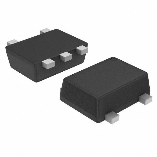
- SMV(SOT-25)和ESV(SOT-553)两种封装类型,具有不同的尺寸和重量。
参数特性:
- 静态偏置电流低(最大2μA,当IOUT=0mA,Tj=-40至85°C)
- 降额电压低(典型值270mV,2.5V输出,IOUT=150mA)
- 输出电压精度高(±1.0%,1.8V ≤ VOUT)
- 具有过流保护和自动放电功能
功能详解:
- 设备支持使用小尺寸陶瓷输入和输出电容(0.1μF),适合高密度板组装。
- 控制引脚可以进行开关控制,高电平开启,低电平关闭。
应用信息:
- 适用于便携式设备,尤其是那些需要高密度板组装的应用。
封装信息:
- 提供SMV(SOT-25)和ESV(SOT-553)两种封装选项,具有不同的尺寸和重量。