TCR3DG series
TOSHIBA CMOS Linear Integrated Circuit Silicon Monolithic
TCR3DG series
300 mA CMOS Low Drop-Out Regulator with inrush current protection circuit
The TCR3DG series are CMOS general-purpose single-output
voltage regulators with an on/off control input, featuring low dropout
voltage, low output noise voltage and low inrush current.
These voltage regulators are available in fixed output voltages
between 1.0 V and 4.5 V and capable of driving up to 300 mA.
They feature over-current protection, thermal shut down function,
Inrush current protection circuit and Auto-discharge function.
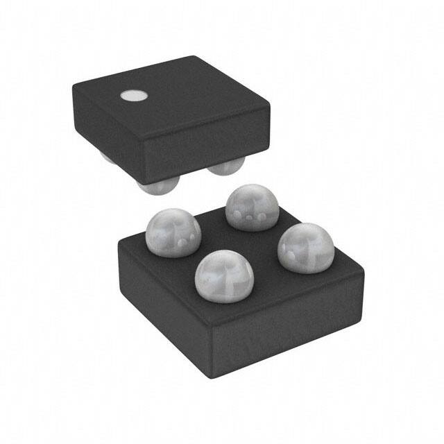
The TCR3DG series are offered in the ultra small package
WCSP4E
WCSP4E(0.645mm x 0.645mm; t 0.40mm). It has a low dropout
voltage of 160 mV (3.2 V output, IOUT = 300 mA) with low output
Weight : 0.34 mg (Typ.)
noise voltage of 38 μVrms (2.5 V output) and a load transient
response of only ⊿VOUT = ±80 mV ( IOUT = 1 mA⇔300 mA, COUT =1.0 μF).
As small ceramic input and output capacitors can be used with the TCR3DG series, these devices are ideal for portable
applications that require high-density board assembly such as cellular phones.
Features
•
Low Drop-Out voltage
VIN-VOUT = 160 mV (Typ.) at 3.2 V-output, IOUT = 300 mA
•
Low output noise voltage
•
VNO = 38 μVrms (Typ.) at 2.5 V-output, IOUT = 10 mA, 10 Hz <
= f <
= 100 kHz
Fast load transient response (⊿VOUT = ±80 mV (Typ.) at IOUT = 1 ⇔ 300 mA, COUT =1.0 μF )
•
High ripple rejection ( R.R = 70 dB (Typ.) at 2.5V-output, IOUT = 10 mA, f =1kHz )
•
Over current protection
•
Thermal shut down function
•
Inrush current protection circuit
•
Auto-discharge function
•
Pull down connection between CONTROL and GND
•
Ceramic capacitors can be used ( CIN = 1.0μF, COUT =1.0 μF )
•
Ultra small package WCSP4E (0.645 mm x 0.645 mm ; t 0.40 mm )
Start of commercial production
2016-03
1
2016-03-14
�TCR3DG series
Absolute Maximum Ratings (Ta = 25°C)
Characteristics
Symbol
Rating
Unit
Input voltage
VIN
6.0
V
Control voltage
VCT
-0.3 to 6.0
V
Output voltage
VOUT
-0.3 to VIN + 0.3
V
Output current
IOUT
300
Power dissipation
PD
800
Operation temperature range
Topr
−40 to 85
°C
Tj
150
°C
Tstg
−55 to 150
°C
Junction temperature
Storage temperature range
mA
(Note1)
mW
Note:
Using continuously under heavy loads (e.g. the application of high temperature/current/voltage and the
significant change in temperature, etc.) may cause this product to decrease in the reliability significantly even
if the operating conditions (i.e. operating temperature/current/voltage, etc.) are within the absolute maximum
ratings and the operating ranges.
Please design the appropriate reliability upon reviewing the Toshiba Semiconductor Reliability Handbook
(“Handling Precautions”/“Derating Concept and Methods”) and individual reliability data (i.e. reliability test
report and estimated failure rate, etc).
Note1:
Rating at mounting on a board
Board material: Glass epoxy(FR4)
Board dimension: 40mm x 40mm (both sides of board), t= 1.6mm
Metal pattern ratio: a surface approximately 50%, the reverse side approximately 50%
Through hole: diameter 0.5mm x 24
Pin Assignment (Top view)
1
2
1
2
A
VIN
VOUT
B
CONTROL
GND
A
B
2
2016-03-14
�TCR3DG series
List of Products Number, Output voltage and Marking
Product No.
Output voltage
Marking
Product No.
(V)(Typ.)
Output voltage
Marking
(V)(Typ.)
TCR3DG10
1.0
E
TCR3DG285*
2.85
R
TCR3DG11*
1.1
F
TCR3DG30*
3.0
T
TCR3DG12
1.2
H
TCR3DG31*
3.1
U
TCR3DG13*
1.3
J
TCR3DG32
3.2
A
TCR3DG135*
1.35
K
TCR3DG33
3.3
B
TCR3DG18*
1.8
L
TCR3DG35*
3.5
V
TCR3DG25*
2.5
P
TCR3DG36*
3.6
C
TCR3DG28*
2.8
W
TCR3DG45*
4.5
D
Please ask your local retailer about the devices with (*) or other output voltages.
Top Marking (top view)
Example: TCR3DG32 (3.2 V output)
GND
VOUT
A
VIN
CONTROL
3
2016-03-14
�TCR3DG series
Electrical Characteristics
(Unless otherwise specified, VIN = VOUT + 1 V, IOUT = 50 mA, CIN = 1.0 μF, COUT = 1.0 μF, Ta = 25°C)
Characteristics
Output voltage accuracy
Input voltage
Symbol
VOUT
VIN
Test Condition
Min
Typ.
Max
Unit
VOUT
很抱歉,暂时无法提供与“TCR3DG135,LF”相匹配的价格&库存,您可以联系我们找货
免费人工找货