TCR3DM series
TOSHIBA CMOS Linear Integrated Circuit Silicon Monolithic
TCR3DM series
300 mA CMOS Low Dropout Regulator with inrush current protection circuit
The TCR3DM series are CMOS general-purpose single-output voltage
regulators with an on/off control input, featuring low dropout voltage, low
output noise voltage and low inrush current.
These voltage regulators are available in fixed output voltages between 1.0
V and 4.5 V and capable of driving up to 300 mA.
They feature over-current protection, over-temperature protection, Inrush
current protection circuit and Auto-discharge function.
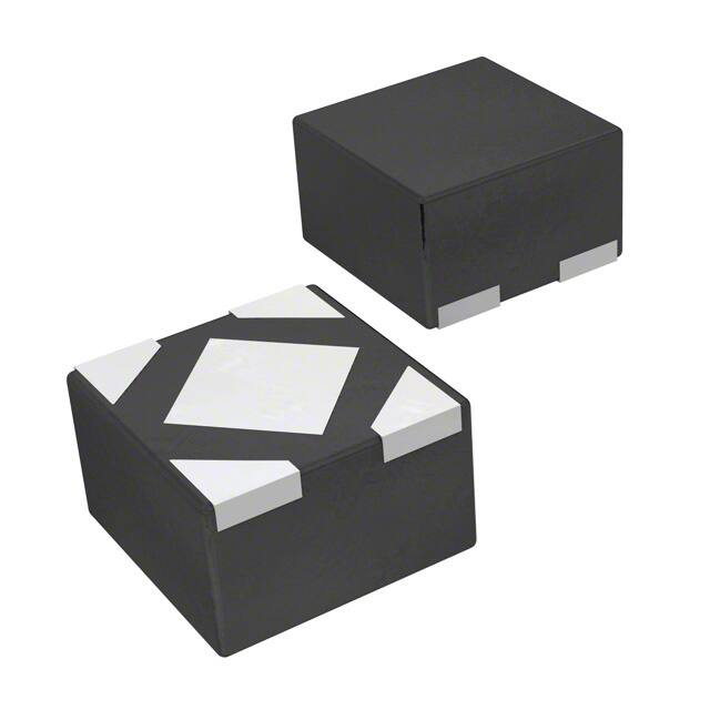
The TCR3DM series are offered in the ultra small plastic mold package
DFN4/DFN4E (1.0 mm x 1.0 mm; t 0.58 mm). It has a low dropout voltage of
210 mV (2.5 V output, IOUT = 300 mA) with low output noise voltage of 38
μVrms (2.5 V output) and a load transient response of only ΔVOUT = ±80 mV
( IOUT = 1 mA⇔300 mA, COUT =1.0 μF).
As small ceramic input and output capacitors can be used with the
TCR3DM series, these devices are ideal for portable applications that require
high-density board assembly such as cellular phones.
BOTTOM VIEW ILLUSTRATION
DFN4/DFN4E
Weight : 1.3 mg ( typ.)
Features
Low Dropout voltage
VDO = 210 mV (typ.) at 2.5 V-output, IOUT = 300 mA
VDO = 270 mV (typ.) at 1.8 V-output, IOUT = 300 mA
VDO = 490 mV (typ.) at 1.2 V-output, IOUT = 300 mA
Low output noise voltage
VNO = 38 μVrms (typ.) at 2.5 V-output, IOUT = 10 mA, 10 Hz ≤ f ≤ 100 kHz
Fast load transient response (ΔVOUT = ±80 mV (typ.) at IOUT = 1 mA ⇔ 300 mA, COUT =1.0 μF)
High ripple rejection (R.R = 70 dB (typ.) at 2.5 V-output, IOUT = 10 mA, f =1 kHz)
Overcurrent protection
Over-temperature protection
Inrush current protection circuit
Auto-discharge
Pull down connection between CONTROL and GND
Ceramic capacitors can be used (CIN = 1.0 μF, COUT =1.0 μF)
Ultra small package DFN4/DFN4E (1.0 mm x 1.0 mm ; t 0.58 mm)
Start of commercial production
2013-03
© 2021
Toshiba Electronic Devices & Storage Corporation
1
2021-09-27
�TCR3DM series
Absolute Maximum Ratings (Ta = 25°C)
Characteristics
Symbol
Rating
Unit
Input voltage
VIN
6.0
V
Control voltage
VCT
-0.3 to 6.0
V
Output voltage
VOUT
-0.3 to VIN + 0.3
V
Output current
IOUT
300
mA
Power dissipation
PD
420
Operating temperature range
Topr
-40 to 85
°C
Tj
150
°C
Tstg
-55 to 150
°C
Junction temperature
Storage temperature range
(Note1)
mW
Note:
Using continuously under heavy loads (e.g. the application of high temperature/current/voltage and the significant
change in temperature, etc.) may cause this product to decrease in the reliability significantly even if the operating
conditions (i.e. operating temperature/current/voltage, etc.) are within the absolute maximum ratings and the
operating ranges.
Please design the appropriate reliability upon reviewing the Toshiba Semiconductor Reliability Handbook
(“Handling Precautions”/“Derating Concept and Methods”) and individual reliability data (i.e. reliability test report
and estimated failure rate, etc).
Note1:
Rating at mounting on a board
Glass epoxy(FR4) board dimension: 40mm x 40mm x 1.6mm, both sides of board.
Metal pattern ratio: a surface approximately 50%, the reverse side approximately 50%
Through hole hall: diameter 0.5mm x 24
Pin Assignment (top view)
VIN
CONTROL
4
3
*
1
2
VOUT
GND
*Center electrode should be connected to GND or Open
© 2021
Toshiba Electronic Devices & Storage Corporation
2
2021-09-27
�TCR3DM series
List of Products Number, Output voltage and Marking
Product No.
Output voltage(V)
Marking
Product No.
Output voltage(V)
Marking
TCR3DM10
1.0
1P0
TCR3DM28
2.8
2P8
TCR3DM105
1.05
1PA
TCR3DM285
2.85
2PD
TCR3DM11
1.1
1P1
TCR3DM30
3.0
3P0
TCR3DM12
1.2
1P2
TCR3DM32
3.2
3P2
TCR3DM13
1.3
1P3
TCR3DM33
3.3
3P3
TCR3DM135
1.35
1PD
TCR3DM35
3.5
3P5
TCR3DM15
1.5
1P5
TCR3DM36
3.6
3P6
TCR3DM18
1.8
1P8
TCR3DM45
4.5
4P5
TCR3DM25
2.5
2P5
Please contact your local Toshiba representative if you are interested in products with other output voltages .
Top Marking (top view)
Example: TCR3DM33 (3.3 V output)
Lot code
3P3
INDEX
© 2021
Toshiba Electronic Devices & Storage Corporation
3
2021-09-27
�TCR3DM series
Electrical Characteristics
(Unless otherwise specified, VIN = VOUT + 1 V, IOUT = 50 mA, CIN = 1.0 μF, COUT = 1.0 μF, Tj = 25°C)
Characteristics
Output voltage accuracy
Input voltage
Symbol
VOUT
VIN
Test Condition
IOUT = 50 mA (Note 2)
Max
Unit
VOUT
很抱歉,暂时无法提供与“TCR3DM105,LF”相匹配的价格&库存,您可以联系我们找货
免费人工找货- 国内价格 香港价格
- 10000+0.8138810000+0.10530
- 国内价格
- 1+1.42895
- 200+0.57014
- 500+0.55113
- 1000+0.54173