TCR5AM series
TOSHIBA CMOS Linear Integrated Circuit Silicon Monolithic
TCR5AM series
500 mA CMOS Ultra Low Drop-Out Regulator
The TCR5AM series are CMOS single-output voltage regulators
with an on/off control input, featuring Ultra low dropout voltage, low
inrush current and fast load transient response.
A differentiating feature is the use of a secondary bias rail as a
reference voltage that allows ultra-low drop-out of 90 mV (Typ.) at
IOUT = 300 mA ( 1.1 V output, VBAT = 3.3 V ).
These voltage regulators are available in fixed output voltages
between 0.55 V and 3.6 V, and capable of driving up to 500 mA.
Other features include over-current protection, over-temperature
protection, Under-voltage-lockout and Auto-discharge function.
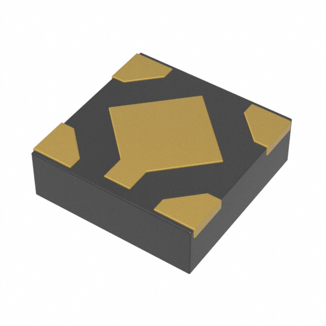
The TCR5AM series are offered in the ultra small plastic mold
package DFN5B (1.2 mm x 1.2 mm; t 0.38 mm).
As small ceramic input and output capacitors can be used with the
TCR5AM series, these devices are ideal for portable applications
that require high-density board assembly such as cellular phones.
BOTTOM VIEW ILLUSTRATION
DFN5B
Weight : 1.4 mg ( Typ.)
Features
•
Low Drop-Out voltage
VIN-VOUT = 90 mV (Typ.) at 1.1 V output, VBAT = 3.3 V , IOUT = 300 mA
•
Low stand-by current ( IB(OFF) = 2 μA (Max) at VBAT = 5.5 V, VCT = 0 V )
•
Low quiescent bias current ( IB = 40μA (Typ.) at VBAT = 5.5 V, IOUT = 0 mA )
•
Wide range Output Voltage line up ( VOUT = 0.55 to 3.6 V )
•
Over-current protection
•
Over-temperature protection
•
Inrush current protection circuit
•
Under-voltage-lockout function
•
Auto-discharge function
•
Pull down connection between CONTROL and GND
•
Ultra small package DFN5B (1.2 mm x 1.2 mm ; t 0.38 mm )
Start of commercial production
2014-12
1
2015-12-15
�TCR5AM series
Absolute Maximum Ratings (Ta = 25°C)
Characteristics
Symbol
Rating
Unit
Bias voltage
VBAT
6.0
V
Input voltage
VIN
6.0
V
Control voltage
VCT
-0.3 to 6.0
V
Output voltage
VOUT
-0.3 to VIN + 0.3
V
Output current
IOUT
DC
500
Pulse
600
(Note 1)
600
(Note 2)
mA
Power dissipation
PD
Operation temperature range
Topr
−40 to 85
°C
Tj
150
°C
Tstg
−55 to 150
°C
Junction temperature
Storage temperature range
Note:
Note 1:
Note 2:
mW
Using continuously under heavy loads (e.g. the application of high temperature/current/voltage and the
significant change in temperature, etc.) may cause this product to decrease in the reliability significantly even
if the operating conditions (i.e. operating temperature/current/voltage, etc.) are within the absolute maximum
ratings and the operating ranges.
Please design the appropriate reliability upon reviewing the Toshiba Semiconductor Reliability Handbook
(“Handling Precautions”/“Derating Concept and Methods”) and individual reliability data (i.e. reliability test
report and estimated failure rate, etc).
100 ms pulse, 50% duty cycle
Rating at mounting on a board
Glass epoxy (FR4) board dimension: 40 mm x 40 mm x 1.6 mm, both sides of board
Metal pattern ratio: a surface approximately 50%, the reverse side approximately 50%
Through hole hall: diameter 0.5 mm x 24
Pin Assignment (top view)
VIN
4
1
VOUT
CONTROL
5*
3
2
VBAT
*Center electrode is GND
2
2015-12-15
�TCR5AM series
List of Products Number, Output voltage and Marking
Product No.
VOUT(V)(Typ.)
Marking
Product No.
VOUT(V)(Typ.)
Marking
TCR5AM055
0.55
0RF
TCR5AM19
1.9
1R9
TCR5AM06
0.6
0R6
TCR5AM20
2.0
2R0
TCR5AM065
0.65
0RG
TCR5AM21
2.1
2R1
TCR5AM07
0.7
0R7
TCR5AM22
2.2
2R2
TCR5AM075
0.75
0RH
TCR5AM23
2.3
2R3
TCR5AM08
0.8
0R8
TCR5AM24
2.4
2R4
TCR5AM085
0.85
0RJ
TCR5AM25
2.5
2R5
TCR5AM09
0.9
0R9
TCR5AM26
2.6
2R6
TCR5AM095
0.95
0RK
TCR5AM27
2.7
2R7
TCR5AM10
1.0
1R0
TCR5AM28
2.8
2R8
TCR5AM105
1.05
1RA
TCR5AM285
2.85
2RJ
TCR5AM11
1.1
1R1
TCR5AM29
2.9
2R9
TCR5AM115
1.15
1RB
TCR5AM295
2.95
2RK
TCR5AM12
1.2
1R2
TCR5AM30
3.0
3R0
TCR5AM125
1.25
1RC
TCR5AM31
3.1
3R1
TCR5AM13
1.3
1R3
TCR5AM32
3.2
3R2
TCR5AM14
1.4
1R4
TCR5AM33
3.3
3R3
TCR5AM15
1.5
1R5
TCR5AM34
3.4
3R4
TCR5AM16
1.6
1R6
TCR5AM35
3.5
3R5
TCR5AM17
1.7
1R7
TCR5AM36
3.6
3R6
TCR5AM18
1.8
1R8
Top Marking (top view)
Example: TCR5AM06 (0.6 V output)
Lot code
0R6
INDEX
3
2015-12-15
�TCR5AM series
Block Diagram
VOUT
VIN
Under
voltage
lockout
VBAT
Thermal
Shut down
+
-
Current
Limit
CONTROL
Control
Logic
Pull down
GND
4
2015-12-15
�TCR5AM series
Electrical Characteristics
(Unless otherwise specified, VIN = VOUT + 0.5 V, IOUT = 50 mA, CIN=CBAT = 1.0 μF, COUT = 2.2 μF)
Tj = -40 to 85°C
(Note 9)
Tj = 25°C
Characteristics
Output voltage accuracy
Bias voltage
Input voltage
Symbol
VOUT
Test Condition
Typ.
Max
Min
Max
VOUT 1.1 V, IOUT = 1 mA
VOUT +
1.4V
―
5.5
VOUT +
1.4V
5.5
V
IOUT = 1 mA,
VOUT +
0.1V
―
VBAT
VOUT +
0.1V
VBAT
V
VBAT
VIN
Min
Unit
Line regulation
Reg・line
VOUT + 0.5 V <
= VIN <
= 5.5 V,
IOUT = 1 mA
―
1
15
―
―
mV
Load regulation
Reg・load
1 mA <
= IOUT <
= 500 mA
―
15
70
―
―
mV
IOUT = 0 mA, VBAT = 5.5 V
(Note 4)(Note 5)
―
40
―
―
68
IOUT = 0 mA, VBAT = 4.2 V
(Note 4)(Note 6)
―
38
―
―
55
VCT = 0 V
―
0.1
―
―
2.0
μA
Quiescent current
Stand-by current
IB
IB (OFF)
μA
ICT
―
―
0.1
―
―
―
μA
VIN-VOUT
IOUT = 300 mA, VBAT = 3.3 V
(Note 7)(Note 8)
―
90
―
―
130
mV
VUVLO
VIN voltage
―
0.5
―
―
0.65
V
TCVO
−40°C <
= Topr <
= 85°C
―
60
―
―
―
ppm/°C
Output noise voltage
VNO
VBAT = 5.5 V, VIN = VOUT + 1 V,
IOUT = 10 mA,
10 Hz <
=f<
= 100 kHz, Ta = 25°C
(Note 7)
―
40
―
―
―
μVrms
Ripple rejection ratio
R.R.
VBAT = 5.5 V, VIN = VOUT + 1 V,
IOUT = 10 mA,
f = 1 kHz, VIN Ripple = 200 mVp-p,
Ta = 25°C
(Note 7)
―
70
―
―
―
dB
Control voltage (ON)
VCT (ON)
―
1.0
―
5.5
1.0
5.5
V
Control voltage (OFF)
VCT (OFF)
―
0
―
0.4
0
0.4
V
RSD
―
―
20
―
―
―
Ω
Control pull down current
Drop-out voltage
Under voltage lockout
Temperature coefficient
Output discharge
on resistance
Note 3:
Note 4:
Note 5:
Note 6:
Note 7:
Note 8:
Stable state with fixed IOUT condition
Except Control pull down current
Over 2.8 V output products
2.8 V and under output products
The 0.6 V output product.
VIN-VOUT = VIN1 - ( VOUT1 x 0.98 )
VOUT1 is the output voltage when VIN = VOUT + 0.5 V.
VIN1 is the input voltage at which the output voltage becomes 98% of VOUT1 after gradually decreasing the
input voltage
Note 9: This parameter is guaranteed by design.
5
2015-12-15
�TCR5AM series
Drop-out voltage
( CIN = 1.0 μF, COUT = 2.2 μF, CBAT = 1.0 μF, Tj = 25°C)
IOUT = 300 mA
Output voltages
VBAT input voltage
IOUT = 500 mA
Min
Typ.
3.3 V
―
90
130
―
150
200
mV
3.3 V
―
90
140
―
150
210
mV
3.3 V
―
90
140
―
150
220
mV
3.3 V
―
90
140
―
150
230
mV
1.0 V
很抱歉,暂时无法提供与“TCR5AM075,LF”相匹配的价格&库存,您可以联系我们找货
免费人工找货- 国内价格
- 1+2.14348
- 200+0.85526
- 500+0.82674
- 1000+0.81260