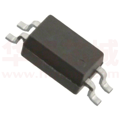
TLP291(SE
TOSHIBA PHOTOCOUPLER GaAs IRED & PHOTO-TRANSISTOR
TLP291(SE
Power Supplies
Programmable Controllers
Hybrid ICs
Unit: mm
TLP291(SE consists of photo transistor optically coupled to a gallium
arsenide infrared emitting diode.
TLP291(SE is housed in the SO4 package, very small and thin coupler.
Since TLP291(SE is guaranteed wide operating temperature (Ta=-55 to
110 ˚C) and high isolation voltage (3750Vrms), it’s suitable for high-density
surface mounting applications such as small switching power supplies and
programmable controllers.
Collector-Emitter Voltage
Current Transfer Ratio
Rank GB
: 80 V (min)
: 50% (min)
: 100% (min)
TOSHIBA
11-3C1
Weight: 0.05 g (typ.)
Isolation Voltage
: 3750 Vrms (min)
Operation temperature: -55 to 110 ˚C
UL recognized
cUL approved
: UL1577, File No. E67349
SEMKO conformity
: EN 60065: 2002,
Pin Configuration
: CSA Component Acceptance Service No.5A,
F ile No. E67349
EN 60950-1: 2001, EN 60335-1: 2002,
BSI conformity
: BS EN 60065: 2002,
BS EN 60950-1: 2006
VDE conformity: EN 60747-5-5
TLP291
1
4
2
3
1:ANODE
2:CATHODE
3:EMITTER
4:COLLECTOR
Construction Mechanical Rating
Creepage distance: 5.0mm(min)
Clearance: 5.0mm(min)
Insulation thickness: 0.4mm(min)
1
2013-05-27
�TLP291(SE
Current Transfer Ratio (CTR) Rank ( Unless otherwise specified, Ta = 25°C)
TYPE
TLP291
Classification
(Note1)
Current Transfer Ratio (%)
(I C / I F )
I F = 5 mA, VCE = 5 V, Ta = 25°C
Min
Max
Marking of Classification
Blank
50
600
Blank, YE, GR, GB, BL, Y+, G, G+,B
Rank Y
50
150
YE
Rank GR
100
300
GR
Rank GB
100
600
GB
Rank BL
200
600
BL
Rank YH
75
150
Y+
Rank GRL
100
200
G
Rank GRH
150
300
G+
Rank BLL
200
400
B
Note1: Specify both the part number and a rank in this format when ordering
(e.g.) rank GB: TLP291 (GB,SE
For safety standard certification, however, specify the part number alone.
(e.g.)TLP291 (GB,SE: TLP291
2
2013-05-27
�TLP291(SE
Absolute Maximum Ratings (Note) (Unless otherwise specified, Ta = 25°C)
CHARACTERISTIC
Input forward current
LED
Input forward current derating (Ta≥90°C)
NOTE
UNIT
IF
50
mA
∆I F /∆ Ta
-1.5
mA /°C
1
A
Input forward current (pulsed )
I FP
Input reverse voltage
VR
5
V
Input power dissipation
PD
100
mW
∆ P D /∆ Ta
-3.0
mW/°C
Tj
125
°C
Collector-emitter voltage
V CEO
80
V
Emitter-collector voltage
V ECO
7
V
IC
50
mA
Input power dissipation derating (Ta ≥ 90°C)
Junction temperature
DETECTOR
RATING
SYMBOL
Collector current
Collector power dissipation
(Note 2)
PC
150
mW
∆P C /∆ Ta
-1.5
mW /°C
Tj
125
°C
Operating temperature range
T opr
-55 to 110
°C
Storage temperature range
T stg
-55 to 125
°C
Lead soldering temperature
T sol
260 (10s)
°C
Total package power dissipation
PT
200
mW
∆P T /∆ Ta
-2.0
mW /°C
3750
Vrms
Collector power dissipation derating(Ta≥25°C)
Junction temperature
Total package power dissipation derating(Ta≥25°C)
Isolation voltage
BV S
(Note3)
Note: Using continuously under heavy loads (e.g. the application of high temperature/current/voltage and the
significant change in temperature, etc.) may cause this product to decrease in the reliability significantly even
if the operating conditions (i.e. operating temperature/current/voltage, etc.) are within the absolute maximum
ratings.
Please design the appropriate reliability upon reviewing the Toshiba Semiconductor Reliability Handbook
(“Handling Precautions”/“Derating Concept and Methods”) and individual reliability data (i.e. reliability test
report and estimated failure rate, etc).
Note2: Pulse width ≤ 100μs, frequency 100Hz
Note3: AC , 1 m inute, R .H.≤60%, D evice considered a two terminal device: LED side pins shorted together and
DETECTOR side pins shorted together.
Electrical Characteristics (Unless otherwise specified, Ta = 25°C)
DETECTOR
LED
CHARACTERISTIC
SYMBOL
TEST CONDITION
MIN
TYP.
MAX
UNIT
1.1
1.25
1.4
V
Input forward voltage
VF
I F = 10 mA
Input reverse current
IR
VR = 5 V
-
-
5
μA
Input capacitance
CT
V = 0 V, f = 1 MHz
-
30
-
pF
Collector-emitter breakdown voltage
V (BR) CEO
I C = 0.5 mA
80
-
-
V
Emitter-collector breakdown voltage
V (BR) ECO
I E = 0.1 mA
7
-
-
V
V CE = 48 V
-
0.01
0.08
μA
V CE = 48 V, Ta = 85°C
-
2
50
μA
V = 0 V, f = 1 MHz
-
10
-
pF
Dark current
Collector-emitter capacitance
I DARK
C CE
3
2013-05-27
�TLP291(SE
Coupled Electrical Characteristics (Unless otherwise specified, Ta = 25°C)
CHARACTERISTIC
Current transfer ratio
Saturated current transfer ratio
Collector-emitter saturation voltage
SYMBOL
I C / IF
I C / I F (sat)
V CE (sat)
TEST CONDITION
MIN
TYP.
MAX
50
-
600
100
-
600
-
60
-
30
-
-
I C = 2.4 mA, IF = 8 mA
-
-
0.3
I C = 0.2 mA, IF = 1 mA
-
0.2
-
-
-
0.3
-
-
10
μA
MIN
TYP.
MAX
UNIT
-
0.8
-
pF
10
-
Ω
3750
-
-
AC , 1 second, in OIL
-
10000
-
DC , 1 minute, in OIL
-
10000
-
Vdc
MIN
TYP.
MAX
UNIT
-
2
-
-
3
-
-
3
-
-
3
-
-
0.5
-
-
25
-
-
40
-
I F = 5 mA, VCE = 5 V
Rank G B
I F = 1 mA, VCE = 0.4 V
Rank GB
Rank GB
OFF-state collector current
I C (off)
V F = 0.7 V, VCE = 48 V
UNIT
%
%
V
Isolation Characteristics (Unless otherwise specified, Ta = 25°C)
CHARACTERISTIC
Total capacitance (input to output)
Isolation resistance
SYMBOL
CS
RS
TEST CONDITION
V S = 0 V, f = 1 MHz
12
V S = 500 V, R.H.≤60%
1×10
AC , 1 minute
Isolation voltage
BV S
14
Vrms
Switching Characteristics (Unless otherwise specified, Ta = 25°C)
CHARACTERISTIC
SYMBOL
Rise time
tr
Fall time
tf
Turn-on time
t on
Turn-off time
t off
Turn-on time
t on
Storage time
ts
Turn-off time
t off
TEST CONDITION
V CC = 10 V, I C = 2 mA
R L = 100Ω
R L = 1.9 kΩ
V CC = 5 V, I F = 16 mA
(Fig.1)
μs
μs
(Fig.1) Switching Time Test Circuit
t on
4
t off
2013-05-27
�TLP291(SE
P C -Ta
Collector power dissipation PC
Input forward current
I F (mA)
(mW)
I F -Ta
This curve shows the
maximum limit to the input
forward current.
Ambient temperature
Ta (˚C)
Ambient temperature
(˚C)
I F -V F
Pules width ≤100μs
IF
Ta=25˚C
1000
Input forward current
Input forward current (pulsed)
IFP (mA)
Ta
(mA)
I FP -D R
10000
This curve shows the maximum
limit to the collector power
dissipation.
100
This curve shows the
maximum limit to the input
forward current (pulsed).
10
-3
10
10
-2
10
-1
10
0
Duty cycle ratio D R
F/
Input forward voltage V F
∆ Ta- I
F
(V)
I FP – V FP
Input forward current (pulsed) I FP
(mA)
Input forward current temperature coefficient
ΔVF /ΔTa (mV/°C)
∆V
110˚C
85˚C
50˚C
25˚C
0˚C
-25˚C
-55˚C
Input forward current I F
(mA)
Pulse width ≤10μs
Repetitive frequency=100Hz
Ta=25°C
Input forward voltage (pulsed) V
FP
(V)
Note: The above characteristics curves are presented for reference only and not guaranteed by production test,
unless otherwise noted
5
2013-05-27
�TLP291(SE
I C -V CE
P C (max)
(mA)
Ta=25˚C
50 mA
I
I
10 mA
I F = 5mA
V CE
30 mA
Collector current
Collector current
15 mA
Collector-emitter voltage
Ta=25˚C
C
50 mA
30 mA
20 mA
C
(mA)
I C -V CE
20 mA
10 mA
5 mA
IF = 2
mA
Collector-emitter voltage
(V)
15 mA
V CE
(V)
IC/IF -IF
Current transfer ratio I C / I F (%)
IC-IF
Collector current
IC
(mA)
Ta=25˚C
V CE =10V
V CE =10V
V CE =5V
V CE =0.4V
V CE =5V
V CE =0.4V
Input forward voltage I F
(mA)
Input forward current I F
V CE (sa t ) - Ta
V CE =48
24V
10V
5V
(V)
V CE(sat)
I
CEO
(μA)
Collector-emitter saturation voltage
I CEO -Ta
Dark current
(mA)
I F =8mA,
I C =2.4mA
Ambient temperature
Ta
(°C)
Ambient temperature
Ta
(°C)
Note: The above characteristics curves are presented for reference only and not guaranteed by production test,
unless otherwise noted
6
2013-05-27
�TLP291(SE
I C - Ta
Collector current I C (mA)
25 mA
10 mA
5 mA
1 mA
I F =0.5mA
V CE =5V
Ambient temperature Ta
(°C)
Sw itch ing t ime - R L
Sw itch ing t ime - Ta
I F =16mA
Ta=25˚C
V CC =5V
I F =16mA
R L =1.9kΩ
V CC =5V
toff
Switching time (μs)
Switching time (μs)
toff
ts
ts
ton
ton
Ambient temperature
Load resistance R L (kΩ)
Ta
(°C)
Note: The above characteristics curves are presented for reference only and not guaranteed by production test,
unless otherwise noted.
7
2013-05-27
�TLP291(SE
Soldering and Storage
1. Soldering
1.1 Soldering
When using a soldering iron or medium infrared ray/hot air reflow, avoid a rise in device temperature as
much as possible by observing the following conditions.
1) Using solder reflow
·Temperature profile example of lead (Pb) solder
(°C)
This profile is based on the device’s
maximum heat resistance guaranteed
value.
Set the preheat temperature/heating
temperature to the optimum temperature
corresponding to the solder paste
type used by the customer within the
described profile.
Package surface temperature
240
210
160
140
less than 30s
60 to 120s
Time
(s)
·Temperature profile example of using lead (Pb)-free solder
(°C)
This profile is based on the device’s
maximum heat resistance guaranteed
value.
Set the preheat temperature/heating
temperature to the optimum temperature
corresponding to the solder paste
type used by the customer within the
described profile.
Package surface temperature
260
230
190
180
60 to 120s
30 to 50s
Time
(s)
Reflow soldering must be performed once or twice.
The mounting should be completed with the interval from the first to the last mountings being 2 weeks.
2) Using solder flow (for lead (Pb) solder, or lead (Pb)-free solder)
· Please preheat it at 150°C between 60 and 120 seconds.
· Complete soldering within 10 seconds below 260°C. Each pin may be heated at most once.
3) Using a soldering iron
Complete soldering within 10 seconds below 260°C, or within 3 seconds at 350°C. Each pin may
be heated at most once.
8
2013-05-27
�