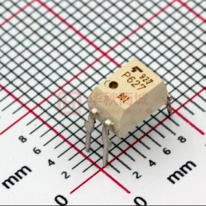
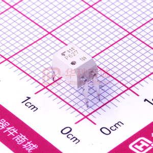
TLP627,TLP627-2,TLP627-4
TOSHIBA PHOTOCOUPLER GaAs IRED & PHOTO-TRANSISTOR
TLP627,TLP627-2,TLP627-4
Unit in mm
PROGRAMMABLE CONTROLLERS DC-OUTPUT MODULE TELECOMMUNICATION
The TOSHIBA TLP627,-2 and -4 consists of a gallium arsenide infrared emitting diode optically coupled to a darlington connected phototransistor which has an integral base-emitter resistor to optimize switching speed and elevated temperature characteristics. The TLP627-2 offers two isolated channels in a eight lead plastic DIP, while the TLP627-4 provide four isolated channels per package. Collector-Emitter Voltage Current Transfer Ratio Isolation Voltage UL Recognized : 300V(Min) : 1000%(Min) : 5000Vrms(Min) : UL1577,File No.E67349
MADE IN JAPAN UL Recognized BSI Approved E67349 7426, 7427 *1 *2 MADE IN THAILAND E152349 7426, 7427 *1 *2
TOSHIBA Weight: 0.26 g
11−5B2
*1 UL1577 *2 BS EN60065: 2002, BS EN60950-1: 2002
TOSHIBA
11−10C4
PIN CONFIGURATION (TOP VIEW)
TLP627 TLP627-2 TLP627-4
Weight: 0.54 g
1 2
1: ANODE 2: CATHODE 3: EMITTER 4:COLLECTOR
4 3
1 2 3 4
1,3: ANODE 2,4: CATHODE 5,7: EMITTER 6,8:COLLECTOR
8 7 6 5
1 2 3 4 5 6 7 8
16 15 14 13 12 11 10 9
TOSHIBA Weight: 1.1 g 11−20A3
1,3,5,7 : ANODE 2,4,6,8 : CATHODE 9,11,13,15 : EMITTER 10,12,14,16 :COLLECTOR
1
2007-10-01
�TLP627,TLP627-2,TLP627-4
Absolute Maximum Ratings (Ta=25°C)
RATING CHARACTERISTIC SYMBOL TLP627 Forward Current Forward Current Derating Pulse Forward Current LED Power Dissipation Power Dissipation Derating (Ta≥25°C,1 Circuit) Reverse Voltage Junction Temperature Collector-Emitter Voltage DETECTOR Emitter -Collector Voltage Collector Current Collector Power Dissipation Collector Power Dissipation Derating Junction Temperature Operating Temperature Range Storage Temperature Range Lead Soldering Temperature (10s) Total Package Power Dissipation Total Package Power Dissipation Derating Isolation Voltage (AC,1min. , R.H.≤60%) (Ta≥25°C,1 Circuit) (Note1) (1 Circuit) (Ta≥25°C,1 Circuit) (1 Circuit) IF ∆IF /°C IFP PD ∆ PD /°C VR Tj VCEO VECO IC PC ∆ Pc /°C Tj Topr Tstg Tsold PT ∆ PT/°C BVS 150(*300) -1.5(*-3.5) 125 −55~100 −55~125 260(10sec) 250(*320) -2.5(*-3.2) 5000 150 -1.5 60 −0.7(Ta≥39°C) TLP627-2 TLP627-4 50 −0.5(Ta≥25°C) UNIT
mA mA /°C A mW mW /°C V °C V V mA
1(100μs pulse,100pps) 100 -1.0 5 125 300 0.3 150 100 -1.0 70 -0.7
mW mW /°C °C °C °C °C mW mW /°C Vrms
*IF=20mA Max Note: Using continuously under heavy loads (e.g. the application of high temperature/current/voltage and the significant change in temperature, etc.) may cause this product to decrease in the reliability significantly even if the operating conditions (i.e. operating temperature/current/voltage, etc.) are within the absolute maximum ratings. Please design the appropriate reliability upon reviewing the Toshiba Semiconductor Reliability Handbook (“Handling Precautions”/“Derating Concept and Methods”) and individual reliability data (i.e. reliability test report and estimated failure rate, etc). (Note1)Device considered a two terminal device : LED side pins Shorted together and DETECTOR side pins shorted
together.
Recommended Operating Conditions
CHARACTERISTIC Supply Voltage Forward Current Collector Current Operating Temperature SYMBOL VCC IF IC Topr MIN. — — — −25 TYP. — 16 — — MAX. 200 25 120 85 UNIT V mA mA °C
Note: Recommended operating conditions are given as a design guideline to obtain expected performance of the device. Additionally, each item is an independent guideline respectively. In developing designs using this product, please confirm specified characteristics shown in this document.
2
2007-10-01
�TLP627,TLP627-2,TLP627-4
Individual Electrical Characteristics (Ta=25°C)
CHARACTERISTIC Forward Voltage LED Reverse Current Capacitance Collector-Emitter Breakdown Voltage DETECTOR Emitter-Collector Breakdown Voltage Collector Dark Current Capacitance Collector to Emitter SYMBOL VF IR CT V(BR)CEO V(BR)ECO ICEO CCE IF = 10 mA VR = 5 V V=0, f=1MHz TEST CONDITION MIN. 1.0 — — 300 0.3 — — — TYP. 1.15 — 30 — — 10 — 10 MAX. 1.3 10 — — — 200 20 — UNIT V μA pF V V nA μA pF
IC = 0.1mA IE = 0.1mA VCE = 200V VCE = 200V , Ta = 85°C V=0 , f=1MHz
Coupled Electrical Characteristics (Ta=25°C)
CHARACTERISTIC Current Transfer Ratio Saturated CTR Collector-Emitter Saturation Voltage SYMBOL IC/IF IC/IF(sat) VCE(sat) TEST CONDITION IF=1mA , VCE=1V IF=10mA , VCE=1V IC=10mA , IF=1mA IC=100mA , IF=10mA MIN. 1000 500 — 0.3 TYP. 4000 — — — MAX. — — 1.0 1.2 UNIT % % V
Isolation Electrical Characteristics (Ta=25°C)
CHARACTERISTIC Capacitance Input to Output Isolation Resistance SYMBOL CS RS TEST CONDITION VS=0 , f=1MHz VS=500V , R.H.≤60% AC, 1minute Isolation Voltage BVs AC, 1second, in oil DC, 1 minute, in oil MIN. — 5×10
10
TYP. 0.8 10
14
MAX. — — — — —
UNIT pF Ω Vrms Vdc
5000 — —
— 10000 10000
3
2007-10-01
�TLP627,TLP627-2,TLP627-4
Switching Characteristics (Ta=25°C)
CHARACTERISTIC Rise Time Fall Time Turn-on Time Turn-off Time Turn-on Time Strage Time Turn-off Time SYMBOL tr tf ton toff tON ts tOFF RL=180Ω (Fig.1) VCC=10V , IF=16mA TEST CONDITION VCC=10V IC=10mA RL=100Ω MIN. — — — — — — — TYP. 40 15 50 15 5 40 80 MAX. — — — — — — — μs UNIT
Fig.1 SWITCHING TIME TEST CIRCUIT
IF RL VCC
VCE
IF VCE 9V VCC
ts
1V tON tOFF
4
2007-10-01
�TLP627,TLP627-2,TLP627-4
5
2007-10-01
�TLP627,TLP627-2,TLP627-4
6
2007-10-01
�TLP627,TLP627-2,TLP627-4
7
2007-10-01
�TLP627,TLP627-2,TLP627-4
RESTRICTIONS ON PRODUCT USE
• The information contained herein is subject to change without notice.
20070701-EN
• TOSHIBA is continually working to improve the quality and reliability of its products. Nevertheless, semiconductor devices in general can malfunction or fail due to their inherent electrical sensitivity and vulnerability to physical stress. It is the responsibility of the buyer, when utilizing TOSHIBA products, to comply with the standards of safety in making a safe design for the entire system, and to avoid situations in which a malfunction or failure of such TOSHIBA products could cause loss of human life, bodily injury or damage to property. In developing your designs, please ensure that TOSHIBA products are used within specified operating ranges as set forth in the most recent TOSHIBA products specifications. Also, please keep in mind the precautions and conditions set forth in the “Handling Guide for Semiconductor Devices,” or “TOSHIBA Semiconductor Reliability Handbook” etc. • The TOSHIBA products listed in this document are intended for usage in general electronics applications (computer, personal equipment, office equipment, measuring equipment, industrial robotics, domestic appliances, etc.).These TOSHIBA products are neither intended nor warranted for usage in equipment that requires extraordinarily high quality and/or reliability or a malfunction or failure of which may cause loss of human life or bodily injury (“Unintended Usage”). Unintended Usage include atomic energy control instruments, airplane or spaceship instruments, transportation instruments, traffic signal instruments, combustion control instruments, medical instruments, all types of safety devices, etc.. Unintended Usage of TOSHIBA products listed in his document shall be made at the customer’s own risk. • The products described in this document shall not be used or embedded to any downstream products of which manufacture, use and/or sale are prohibited under any applicable laws and regulations. • The information contained herein is presented only as a guide for the applications of our products. No responsibility is assumed by TOSHIBA for any infringements of patents or other rights of the third parties which may result from its use. No license is granted by implication or otherwise under any patents or other rights of TOSHIBA or the third parties. • GaAs(Gallium Arsenide) is used in this product. The dust or vapor is harmful to the human body. Do not break, cut, crush or dissolve chemically. • Please contact your sales representative for product-by-product details in this document regarding RoHS compatibility. Please use these products in this document in compliance with all applicable laws and regulations that regulate the inclusion or use of controlled substances. Toshiba assumes no liability for damage or losses occurring as a result of noncompliance with applicable laws and regulations.
8
2007-10-01
�


 工商网监
湘ICP备2023018690号
工商网监
湘ICP备2023018690号