TLP715
TOSHIBA PHOTOCOUPLER
GaAℓAs IRED & PHOTO-IC
TLP715
Isolated Bus Drivers
High Speed Line Receivers
Microprocessor System Interfaces
Unit: mm
4.58±0.25
Buffer logic output (totem pole output)
Guaranteed performance over temperature: −40 to 100°C
Power supply voltage: 4.5 to 20 V
Input current: IFLH = 3 mA (max)
Switching time ( tpLH / tpHL): 250 ns (max)
Common-mode transient immunity: ±10 kV / μs (min)
Isolation voltage: 5000 Vrms (min)
UL recognized
UL1577, File No.E67349
c-UL recognized
CSA Component Acceptance Service No. 5A, File No.E67349
Option (D4)
TÜV recognized / VDE under application: DIN EN60747-5-5
Maximum Operating Insulation Voltage: 890 VPK
Highest Permissible Over Voltage : 8000 VPK
(Note): When a EN60747-5-5 approved type is needed,
Please designate “Option(D4)”
Construction Mechanical Rating
7.62 mm pitch
TLPXXX type
10.16 mm pitch
TLPXXXF type
7.0 mm (min)
7.0 mm (min)
0.4 mm (min)
8.0 mm (min)
8.0 mm (min)
0.4 mm (min)
Creepage Distance
Clearance
Insulation Thickness
+0.25
4.0 −0.20
7.62±0.25
−0.05
0.25± +0.10
1 2 3
3.65 +0.15
−0.25
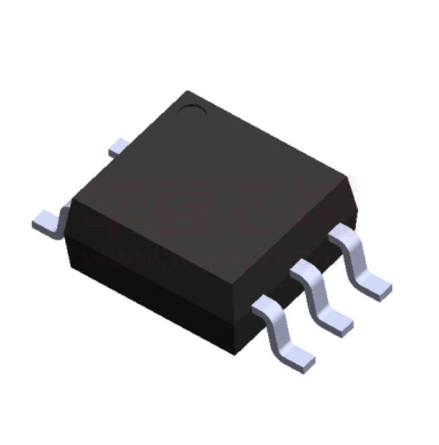
The Toshiba TLP715 consists of a GaAℓAs light-emitting diode and an
integrated high-gain, high-speed photodetector. This unit is a 6-pin SDIP. The
TLP715 is 50% smaller than the 8-PIN DIP and meets the reinforced insulation
class requirements of international safety standards. Therefore the mounting
area can be reduced in equipment requiring safety standard certification.
The detector has a totem pole output stage to provide both source and sink
driving. The detector IC has an internal shield that provides a guaranteed
common-mode transient immunity of 10 kV / μs.
The TLP715 is buffer logic type. For inverter logic type, the TLP718 is in
line-up.
6.8±0.25
6 5 4
1.27±0.2
1.25±0.25
0.4±0.1
9.7±0.3
11-5J1
TOSHIBA
11-5J1
Weight: 0.26 g (t yp .)
Pin Configuration (Top View)
VCC
1
2
6
5
GND
3
SHIELD
1: ANODE
2: N.C.
3: CATHODE
4: GND
4
5: VO (Output)
6: VCC
Schematic
ICC
6
IF
VCC
Tr1
1+
IO
VF
3-
Tr2
5
VO
Truth Table
GND
Input
LED
Tr1
Tr2
Output
H
ON
ON
OFF
H
L
OFF
OFF
ON
L
4
SHIELD
0.1 μF bypass capacitor must be
connected between pins 6 and 4. (Note 5)
Start of commercial production
2008/11
1
2014-09-01
�TLP715
Absolute Maximum Ratings (Ta = 25°C)
CHARACTERISTIC
SYMBOL
RATING
UNIT
IF
20
mA
∆IF/∆Ta
−0.48
mA/°C
IFPT
1
A
Reverse Voltage
VR
5
V
Junction Temperature
Tj
125
°C
Output Current 1 (Ta ≤ 25°C)
IO1
25 / −15
mA
Output Current 2 (Ta ≤ 100°C)
IO2
13 / −13
mA
Output Voltage
VO
−0.5 to 20
V
Supply Voltage
VCC
−0.5 to 20
V
Tj
125
°C
Operating Temperature Range
Topr
−40 to 100
°C
Storage Temperature Range
Tstg
−55 to 125
°C
Lead Solder Temperature (10 s)
Tsol
260
°C
Isolation Voltage (AC,1 minute, R.H. ≤ 60%, Ta = 25°C) (Note 2)
BVS
5000
Vrms
Forward Current
(Ta ≤ 83°C)
DETECTOR
LED
Forward Current Derating
(Ta ≥ 83°C)
Peak Transient Forward Current
(Note 1)
Junction Temperature
Note: Using continuously under heavy loads (e.g. the application of high temperature/current/voltage and the
significant change in temperature, etc.) may cause this product to decrease in the reliability significantly even if
the operating conditions (i.e. operating temperature/current/voltage, etc.) are within the absolute maximum
ratings.
Please design the appropriate reliability upon reviewing the Toshiba Semiconductor Reliability Handbook
(“Handling Precautions”/“Derating Concept and Methods”) and individual reliability data (i.e. reliability test
report and estimated failure rate, etc).
Note 1: Pulse width PW ≤ 1μs, 300pps.
Note 2: Device Considered a two terminal device: pins 1, 2 and 3 shorted together and pins 4, 5 and 6 shorted
together.
Recommended Operating Conditions
CHARACTERISTIC
SYMBOL
MIN
TYP.
MAX
UNIT
Input Current, ON
IF (ON)
4.5
−
10
mA
Input Voltage, OFF
VF (OFF)
0
−
0.8
V
Supply Voltage*
VCC
4.5
−
20
V
Operating Temperature
Topr
-40
−
100
°C
* This item denotes operating ranges, not meaning of recommended operating conditions.
Note: Recommended operating conditions are given as a design guideline to obtain expected performance of the
device. Additionally, each item is an independent guideline respectively. In developing designs using this
product, please confirm specified characteristics shown in this document.
2
2014-09-01
�TLP715
Electrical Characteristics
(Unless otherwise specified, Ta =−40 to 100°C, VCC = 4.5 to 20 V)
CHARACTERISTIC
SYMBOL
TEST
CIRCUIT
CONDITION
MIN
TYP. *
MAX
UNIT
1.4
1.6
1.7
V
VF
−
IF = 5 mA , Ta = 25°C
∆VF/∆Ta
−
IF = 5 mA
−
−2.0
−
mV/°C
Input reverse current
IR
−
VR = 5 V , Ta = 25°C
−
−
10
μA
Input capacitance
CT
−
V = 0 V, f = 1 MHz, Ta = 25°C
−
45
−
pF
Logic LOW output voltage
VOL
1
IOL = 3.5 mA, VF = 0.8 V
−
0.2
0.6
V
Input forward voltage
Temperature coefficient of
forward voltage
Logic HIGH output voltage
VOH
(Note3)
2
IOH = −2.6 mA,
VCC = 4.5 V
2.7
3.5
−
IF=5 mA
VCC = 20 V
17.4
19
−
V
Logic LOW supply current
ICCL
3
VF = 0V
−
−
3.0
mA
Logic HIGH supply current
ICCH
4
IF = 5 mA
−
−
3.0
mA
IOSL
5
VF = 0V
VCC = VO = 5.5 V
15
80
−
VCC = VO = 20 V
20
90
−
IOSH
6
VCC = 5.5 V
−5
-15
−
VO = GND VCC = 20 V
−10
−20
−
IFLH
−
IO = -2.6 mA, VO > 2.4 V
−
0.4
3
mA
VFHL
−
IO = 3.5 mA, VO < 0.6V
0.8
−
−
V
IHYS
−
VCC = 5 V
−
0.05
−
mA
Logic
LOW
short
output current
circuit
(Note4)
Logic HIGH short circuit
output current
(Note4)
Input current logic HIGH
output
Input voltage logic LOW
output
Input current hysteresis
IF = 5mA,
mA
mA
* All typical values are at Ta=25°C, VCC=5 V unless otherwise specified
Note 3: VOH = VCC –VO [V]
Note 4: Duration of output short circuit time should not exceed 10 ms.
Note 5: A ceramic capacitor (0.1 μF) should be connected from pin 6 to pin 4 to stabilize the operation of the high
gain linear amplifier. Failure to provide the bypassing may impair the switching property. The total lead
length between capacitor and coupler should not exceed 1 cm.
Isolation Characteristics (Ta = 25°C)
CHARACTERISTIC
SYMBOL
TEST CONDITION
MIN
TYP.
MAX
UNIT
−
1.0
−
pF
−
Ω
Capacitance input to output
CS
V = 0 V, f = 1 MHz
(Note 2)
Isolation resistance
RS
R.H. ≤ 60%, VS = 500 V
(Note 2) 1×10
AC, 1 minute
Isolation voltage
BVS
12
10
14
5000
−
−
AC, 1 second, in oil
−
10000
−
DC, 1 minute, in oil
−
10000
−
3
Vrms
Vdc
2014-09-01
�TLP715
Switching Characteristics
(Unless otherwise specified, Ta = −40 to 100°C, Vcc = 4.5 to 20 V)
TEST
SYMBOL CIRCUIT
CHARACTERISTIC
Propagation delay time
to logic HIGH output
Propagation delay time
to logic LOW output
CONDITION
MIN
TYP. *
MAX
UNIT
tpLH
IF = 0 → 3 mA
30
120
250
ns
tpHL
IF = 3 → 0 mA
30
120
250
ns
−
−
220
ns
Switching time dispersion
|tpLH-
between ON and OFF
tpHL|
Rise Time (10 – 90 %)
tr
IF = 0 → 3 mA, VCC = 5 V
−
30
−
ns
Fall Time (90 – 10 %)
tf
IF = 3 → 0 mA, VCC = 5 V
−
30
−
ns
10000
−
−
V/μs
−10000
−
−
V/μs
Common-mode transient
7,8
−
VCM = 1000 Vp-p, IF = 5 mA,
CMH
Immunity at HIGH level output
VCC = 20 V, Ta = 25°C
9
Common-mode transient
VCM = 1000 Vp-p, IF = 0 mA,
CML
Immunity at LOW level output
VCC = 20 V, Ta = 25°C
*All typical values are at Ta = 25°C.
TEST CIRCUIT 1: VOL
TEST CIRCUIT 2: VOH
IF
→
VCC
1
6
2
5
VF
GND
3
SHIELD
V
VCC
1
0.1μF
VOL IOL
↑
6
V
VO
↑
IOH
Vcc
↑
Vcc
2
5
0.1μF
GND
4
3
SHIELD
4
VOH=VCC –VO [V]
TEST CIRCUIT 3: ICCL
TEST CIRCUIT 4: ICCH
ICCL
VCC
1
IF
→
A
1
6
Vcc
2
5
VCC
Vcc
2
5
SHIELD
3
4
TEST CIRCUIT 5: IOSL
→
6
5
GND
3
SHIELD
4
IOSL
VCC
1
0.1μF
6
↑
A
2
SHIELD
TEST CIRCUIT 6: IOSH
IF
VCC
1
0.1μF
GND
GND
3
A
6
↑
0.1μF
ICCH
Vo
A
2
Vcc
5
GND
4
3
4
0.1μF
SHIELD
IOSH
Vo
Vcc
4
2014-09-01
�TLP715
TEST CIRCUIT 7: Switching Time Test Circuit
IF=3 mA(P.G)
(f=50 kHz , duty=50%
less than tr = tf = 5ns )
IF
50%
Vcc
IF
0.1μF
tp LH
Vcc
Vo
tp HL
90%
GND
CL
SHIELD
VOH
90%
1.3V
10%
1.3V
10%
Vo
tr
VOL
tf
CL: stray capacitance of probe and wiring (to 15 pF)
TEST CIRCUIT 8: Switching Time Test Circuit
IF=3 mA(P.G)
(f=50 kHz , duty=50%
less than tr = tf = 5ns )
Vcc
Vo
5V
IF
50%
Vcc
620Ω
IF
tp LH
0.1μF
tp HL
VOH
GND
CL
SHIELD
5kΩ
1.3V
1.3V
Vo
VOL
CL: stray capacitance of probe and wiring (to 15 pF)
TEST CIRCUIT 9: Common-Mode Transient Immunity Test Circuit
IF
→
SW
A
B
1000V
6
1
90%
Vcc
2
5
3
GND
4
0.1μF
Vo
VCM
10%
tr
Vcc
CMH
・SW A: I F =5mA
SHIELD
VCM
+
tf
17V
Vo
-
1V
CML
・SW B: I F =0mA
800( V )
CM =
L t (μs)
r
800( V )
CM = −
H
t f (μs)
CMH (CML) is the maximum rate of rise (fall) of the common mode voltage that can be sustained with the
output voltage in the high (low) state.
5
2014-09-01
�TLP715
EN60747-5-5 Option:(D4)
Types
: TLP715, TLP715F
Type designations for “option: (D4)”, which are tested under EN60747 requirements.
Ex.: TLP715 (D4-TP,F)
D4 : EN60747 option
TP : Standard tape & reel type
F : [[G]]/RoHS COMPATIBLE
Note: Use TOSHIBA standard type number for safety standard application.
Ex.: TLP715 (D4-TP,F) → TLP715
EN60747 Isolation Characteristics
Description
Symbol
Rating
Unit
Application classification
for rated mains voltage≤300Vrms
for rated mains voltage≤600Vrms
Climatic classification
Pollution degree
TLPxxx type
Maximum operating insulation voltage
40/ 100 / 21
—
2
—
890
VIORM
TLPxxxFtype
Vpk
1140
TLPxxx type
Input to output test voltage, method A
Vpr=1.5×VIORM, type and sample test
tp=10s, partial discharge