TOSHIBA Original CMOS 16-Bit Microcontroller
TLCS-900/L1 Series
TMP91FY42FG
Semiconductor Company
�Preface
Thank you very much for making use of Toshiba microcomputer LSIs.
Before use this LSI, refer the section, “Points of Note and Restrictions”.
Especially, take care below cautions.
�TMP91FY42
CMOS 16-Bit Microcontrollers
TMP91FY42FG
1.
Outline and Features
TMP91FY42F is a high-speed 16-bit microcontroller designed for the control of various mid- to
large-scale equipment.
TMP91FY42FG comes in a 100-pin flat package.
Listed below are the features.
(1) High-speed 16-bit CPU (900/L1 CPU)
•
Instruction mnemonics are upward-compatible with TLCS-90/900
•
General-purpose registers and register banks
•
16 Mbytes of linear address space
•
16-bit multiplication and division instructions; bit transfer and arithmetic instructions
•
Micro DMA: 4-channels (593 ns/2 bytes at 27 MHz)
(2) Minimum instruction execution time: 148 ns (at 27 MHz)
RESTRICTIONS ON PRODUCT USE
060925EBP
• The information contained herein is subject to change without notice. 021023_D
• TOSHIBA is continually working to improve the quality and reliability of its products. Nevertheless, semiconductor
devices in general can malfunction or fail due to their inherent electrical sensitivity and vulnerability to physical
stress. It is the responsibility of the buyer, when utilizing TOSHIBA products, to comply with the standards of safety
in making a safe design for the entire system, and to avoid situations in which a malfunction or failure of such
TOSHIBA products could cause loss of human life, bodily injury or damage to property.
In developing your designs, please ensure that TOSHIBA products are used within specified operating ranges as
set forth in the most recent TOSHIBA products specifications. Also, please keep in mind the precautions and
conditions set forth in the “Handling Guide for Semiconductor Devices,” or “TOSHIBA Semiconductor Reliability
Handbook” etc. 021023_A
• The TOSHIBA products listed in this document are intended for usage in general electronics applications (computer,
personal equipment, office equipment, measuring equipment, industrial robotics, domestic appliances, etc.). These
TOSHIBA products are neither intended nor warranted for usage in equipment that requires extraordinarily high
quality and/or reliability or a malfunction or failure of which may cause loss of human life or bodily injury
(“Unintended Usage”). Unintended Usage include atomic energy control instruments, airplane or spaceship
instruments, transportation instruments, traffic signal instruments, combustion control instruments, medical
instruments, all types of safety devices, etc. Unintended Usage of TOSHIBA products listed in this document shall
be made at the customer’s own risk. 021023_B
• The products described in this document shall not be used or embedded to any downstream products of which
manufacture, use and/or sale are prohibited under any applicable laws and regulations. 060106_Q
• The information contained herein is presented only as a guide for the applications of our products. No responsibility
is assumed by TOSHIBA for any infringements of patents or other rights of the third parties which may result from its
use. No license is granted by implication or otherwise under any patent or patent rights of TOSHIBA or others.
021023_C
• The products described in this document are subject to foreign exchange and foreign trade control laws. 060925_E
• For a discussion of how the reliability of microcontrollers can be predicted, please refer to Section 1.3 of the chapter
entitled Quality and Reliability Assurance/Handling Precautions. 030619_S
This product uses the Super Flash® technology under the license of Silicon Storage Technology,Inc.
Super Flash® is a registered trademark of Silicon Storage Technology,Inc.
91FY42-1
2006-11-08
�TMP91FY42
(3) Built-in RAM: 16 Kbytes
Built-in ROM: 256 Kbytes Flash memory
4 Kbytes mask ROM (used for booting)
(4) External memory expansion
•
Expandable up to 16 Mbytes (shared program/data area)
•
Can simultaneously support 8-/16-bit width external data bus
… Dynamic data bus sizing
(5) 8-bit timers: 8 channels
(6) 16-bit timer/event counter: 2 channels
(7) General-purpose serial interface: 2 channels
•
UART/ Synchronous mode: 2 channels
•
IrDA ver1.0 (115.2 kbps) supported: 1 channel
(8) Serial bus interface: 1 channel
•
I2C bus mode/clock synchronous Select mode
(9) 10-bit AD converter (built-in sample hold circuit) : 8 channels
(10) Watchdog timer
(11) Special timer for clock
(12) Chip Select/Wait controller: 4 channels
(13) Interrupts: 45 interrupts
•
9 CPU interrupts: Software interrupt instruction and illegal instruction
•
26 internal interrupts:
•
10 external interrupts:
Seven selectable priority levels
(14) Input/Output ports: 81 pins
(15) Standby function
Three HALT modes: IDLE2 (programmable), IDLE1, STOP
(16) Clock controller
•
Clock Gear function: Select a high-frequency clock (fc to fc/16)
•
Special timer for CLOCK (fs = 32.768 kHz)
(17) Operating voltage
•
VCC = 2.7 V to 3.6 V (fc max = 27 MHz, flash memory read operation)
•
VCC = 3.0 V to 3.6 V (fc max = 27 MHz, flash memory erase/program operations)
(18) Package
•
100-pin LQFP: LQFP100-P-1414-0.50F
Note: This LSI does not build in Clock doubler (DFM.)
91FY42-2
2006-11-08
�TMP91FY42
ADTRG (P53)
AN0 to AN7
(P50 to P57)
AVCC, AVSS
VREFH, VREFL
TXD0 (P90)
RXD0 (P91)
SCLK0/ CTS0 (P92)
TXD1 (P93)
RXD1 (P94)
SCLK1/ CTS1 (P95)
DVCC [3]
DVSS [3]
X1
X2
CPU (TLCS-900/L1)
10-Bit 8CH
AD
Converter
SIO/UART/IrDA
(SIO0)
XWA
XBC
XDE
XHL
XIX
XIY
XIZ
XSP
W A
B C
D E
H L
IX
IY
IZ
SP
32 bits
SR
F
PC
SIO/UART
(SIO1)
H-OSC
Clock Gear
Clock doubler
L-OSC
RESET
AM0
AM1
ALE
Port 0
Port 1
SCK (P60)
SO/SDA (P61)
SI / SCL (P62)
Serial Bus
Interface
(SBI)
Watchdog
Timer (WDT)
Port 2
TA0IN (P70)
8-Bit Timer
(TMRA0)
Special timer
for CLOCK
Port 3
TA1OUT (P71)
8-Bit Timer
(TMRA1)
16-KB RAM
8-Bit Timer
(TMRA2)
TA3OUT (P72)
8-Bit Timer
(TMRA3)
TA4IN (P73)
8-Bit Timer
(TMRA4)
TA5OUT (P74)
TA7OUT (P75)
SCOUT(P64), P65, P66
Port A
PA4 to PA7
Controller
(4-BLOCK)
8-Bit Timer
(TMRA5)
Interrupt
Controller
8-Bit Timer
(TMRA6)
16-Bit Timer
(TMRB0)
8-Bit Timer
(TMRA7)
4-KB BOOT ROM
(P00 to P07)
AD0 to AD7
(P10 to P17)
AD8/A8 to AD15/A15
(P20 to P27)
A0/A16 to A7/A23
RD (P30)
WR (P31)
HWR (P32)
BUSRQ (P34)
BUSAK (P35)
R/ W (P36)
BOOT (P37)
Port 6
CS/WAIT
256-KB FLASH
E2PROM
EMU0
EMU1
XT1 (P96)
XT2 (P97)
16-Bit Timer
(TMRB1)
(
(P40 to P43)
CS0 to CS3
WAIT (P33)
NMI
INT0 (P64)
INT1 to INT4
(PA0 to PA3)
TB0IN0/INT5 (P80)
TB0IN1/INT6 (P81)
TB0OUT0 (P82)
TB0OUT1 (P83)
TB1IN0/INT7 (P84)
TB1IN1/INT8 (P85)
TB1OUT0 (P86)
TB1OUT1 (P87)
): Initial function after reset
Figure 1.1 TMP91FY42F Block Diagram
91FY42-3
2006-11-08
�TMP91FY42
2.
Pin Assignment and Pin Functions
The assignment of input/output pins for the TMP91FY42, their names and functions are as
follows:
2.1
Pin Assignment Diagram
Figure 2.1.1 shows the pin assignment of the TMP91FY42.
88 P65
DVCC
89
87 P64/SCOUT
P66
90
86 P63/INT0
DVSS
91
85 P62/SI/SCL
P50/AN0
92
84 P61/SO/SDA
P51/AN1
93
83 P60/SCK
P52/AN2
94
82 P43/CS3
P53/AN3/ADTRG 95
81 P42/CS2
P54/AN4
96
80 P41/CS1
P55/AN5
97
79 P40/CS0
P56/AN6
98
78 P37/BOOT
P57/AN7
99
77 P36/R/W
VREFH
100
76 P35/BUSAK
VREFL
1
75 P34/BUSRQ
AVSS
2
74 P33/WAIT
AVCC
3
73 P32/HWR
P70/TA0IN
4
72 P31/WR
P71/TA1OUT
5
71 P30/RD
P72/TA3OUT
6
70 P27/A7/A23
P73/TA4IN
7
69 P26/A6/A22
P74/TA5OUT
8
68 P25/A5/A21
P75/TA7OUT
9
67 P24/A4/A20
P80/TB0IN0/INT5 10
66 P23/A3/A19
P81/TB0IN1/INT6 11
P82/TB0OUT0
12
P83/TB0OUT1
13
65 P22/A2/A18
Top view
QFP100
64 DVCC
63 NMI
P84/TB1IN0/INT7 14
62 DVSS
P85/TB1IN1/INT8 15
16
61 P21/A1/A17
60 P20/A0/A16
P87/TB1OUT1
17
59 P17/AD15/A15
P90/TXD0
18
58 P16/AD14/A14
P91/RXD0
19
57 P15/AD13/A13
P92/SCLK0/CTS0 20
56 P14/AD12/A12
P93/TXD1
21
55 P13/AD11/A11
P94/RXD1
22
54 P12/AD10/A10
P86/TB1OUT0
P95/SCLK1/CTS1 23
AM0
24
53 P11/AD9/A9
52 P10/AD8/A8
DVCC
25
51 P07/AD7
X2
26
50 P06/AD6
DVSS
27
49 P05/AD5
X1
28
48 P04/AD4
AM1
29
47 P03/AD3
RESET
P96/XT1
30
31
46 P02/AD2
P97/XT2
32
44 P00/AD0
EMU0
33
43 ALE
EMU1
34
42 PA7
PA0/INT1
35
41 PA6
PA1/INT2
36
40 PA5
PA2/INT3
37
39 PA4
45 P01/AD1
38 PA3/INT4
Figure 2.1.1 Pin assignment diagram (100-pin LQFP)
91FY42-4
2006-11-08
�TMP91FY42
2.2
Pin Names and Functions
The names of the input/output pins and their functions are described below.
Table 2.2.1 Pin names and functions.
Table 2.2.1 Pin names and functions (1/3)
Pin Name
P00∼P07
Number
of Pins
8
AD0∼AD7
P10∼P17
8
AD8∼AD15
A8∼A15
P20∼P27
I/O
Functions
I/O
Port 0: I/O port that allows I/O to be selected at the bit level
I/O
Address and data (lower): Bits 0 to 7 of address and data bus
I/O
Port 1: I/O port that allows I/O to be selected at the bit level
I/O
Address and data (upper): Bits 8 to 15 for address and data bus
Output
8
I/O
Address: Bits 8 to 15 of address bus
Port 2: I/O port that allows I/O to be selected at the bit level
A0∼A7
Output
A16∼A23
Output
Address: Bits 16 to 23 of address bus
Output
Port 30: Output port
Output
Read: Strobe signal for reading external memory
P30
1
RD
Address: Bits 0 to 7 of address bus
This port output RD signal also case of reading internal-area by setting P3
= 0 and P3FC = 1.
P31
1
WR
P32
1
Port 31: Output port
Output
Write: Strobe signal for writing data to pins AD0 to AD7
I/O
Output
HWR
P33
Output
1
I/O
Input
WAIT
Port 32: I/O port (with pull-up resistor)
High Write: Strobe signal for writing data to pins AD8 to AD15
Port 33: I/O port (with pull-up resistor)
Wait: Pin used to request CPU bus wait
((1+N) WAIT mode)
P34
1
Input
BUSRQ
P35
I/O
1
I/O
Port 34: I/O port (with pull-up resistor)
Bus Request: Signal used to request Bus Release
Port 35: I/O port (with pull-up resistor)
Output
Bus Acknowledge: Signal used to acknowledge Bus Release
1
I/O
Output
Port 36: I/O port (with pull-up resistor)
Read/Write: 1 represents Read or Dummy cycle; 0 represents Write cycle.
P37
BOOT
1
I/O
Input
P40
1
I/O
Output
Port 40: I/O port (with pull-up resistor)
Chip Select 0: Outputs 0 when address is within specified address area
1
I/O
Output
Port 41: I/O port (with pull-up resistor)
Chip Select 1: Outputs 0 if address is within specified address area
1
I/O
Output
Port 42: I/O port (with pull-up resistor)
Chip Select 2: Outputs 0 if address is within specified address area
1
I/O
Output
Port 43: I/O port (with pull-up resistor)
Chip Select 3: Outputs 0 if address is within specified address area
8
Input
Port 5: Pin used to input port
Input
Analog input: Pin used to input to AD converter
Input
AD Trigger: Signal used to request start of AD converter (Shared with53 pin)
BUSAK
P36
R/W
CS0
P41
CS1
P42
CS2
P43
CS3
P50∼P57
AN0∼AN7
ADTRG
Port 36: I/O port (with pull-up resistor)
This pin sets single boot mode.
When released reset, Single boot mode is started at P37=Low level.
91FY42-5
2006-11-08
�TMP91FY42
Table 2.2.1 Pin names and functions (2/3)
Pin Name
P60
Number
of Pins
1
SCK
P61
1
SO
I/O
Functions
I/O
Port 60: I/O port
I/O
Serial bus interface clock in SIO Mode
I/O
Port 61: I/O port
Output
SDA
Serial bus interface send data at SIO mode
2
I/O
Serial bus interface send/recive data at I C bus mode
I/O
Port 62: I/O port
Open-drain output mode by programmable
P62
1
SI
Input
SCL
I/O
Serial bus interface recive data at SIO mode
2
Serial bus interface clock I/O data at I C bus mode
Open-drain output mode by programmable
P63
1
INT0
I/O
Input
Port 63: I/O port
Interrupt Request Pin 0: Interrupt request pin with programmable level /
rising edge / falling edge
P64
1
SCOUT
I/O
Output
Port 64: I/O port
System Clock Output: Outputs fFPH or fs clock.
P65
1
I/O
Port 65 I/O port
P66
1
I/O
Port 66 I/O port
P70
1
I/O
Port 70I/O port
TA0IN
P71
Input
1
TA1OUT
P72
1
TA3OUT
P73
1
1
I/O
Output
1
TA7OUT
P80
I/O
Input
TA5OUT
P75
I/O
Output
TA4IN
P74
I/O
Output
I/O
Output
1
I/O
8bitt timer 0 input:: Timer 0 input
Port 71I/O port
8-bit timer 1 output: Timer 0 or Timer 1 output
Port 72I/O port 8bit
8-bit timer 3 output: Timer 2 or Timer 3 output
Port 73: I/O port
8-bit timer 4 input: Timer 4 input
Port 74: I/O port
8-bit timer 5 output: Timer 4 or Timer 5 output
Port 75: I/O port
88-bit timer 7 output: Timer 6 or Timer 7 output
Port 80: I/O port
TB0IN0
Input
16bit timer 0 input 0: 16bit Timer 0 count / capture trigger input
INT5
Input
Interrupt Request Pin 5: Interrupt request pin with programmable rising edge
/ falling edge.
P81
1
I/O
Port 81: I/O port
TB0IN1
Input
16bit timer 0 input 1: 16bit Timer 0 count / capture trigger input
INT6
Input
Interrupt Request Pin 6: Interrupt request on rising edge
P82
1
TB0OUT0
P83
Output
1
TB0OUT1
P84
I/O
I/O
Output
1
I/O
Port 82: I/O port
16bit timer 0 output 0: 16bit Timer 0 output
Port 83: I/O port
16bit timer 0 output 1: 16bit Timer 0 output
Port 84: I/O port
TB1IN0
Input
16bit timer 1 input 0: 16bit Timer 1 count / capture trigger input
INT7
Input
Interrupt Request Pin 7: Interrupt request pin with programmable rising edge
/ falling edge.
P85
1
I/O
Port 85: I/O port
TB1IN1
Input
16bit timer 1 input 1: 16bit Timer 1 count / capture trigger input
INT8
Input
Interrupt Request Pin 8: Interrupt request on rising edge
P86
1
TB1OUT0
P87
TB1OUT1
I/O
Output
1
I/O
Output
Port 86: I/O port
16bit timer 1 output 0: 16bit Timer 1 output 16bit
Port 87: I/O port
16bit timer 1 output 1: 16bit Timer 1 output 16bit 16bit
91FY42-6
2006-11-08
�TMP91FY42
Table 2.2.1 Pin names and functions (3/3)
Pin Name
P90
Number
of Pins
1
TXD0
P91
1
1
1
1
1
I/O
I/O
Input
CTS1
1
XT1
I/O
Input
1
XT2
PA0∼PA3
I/O
Input
SCLK1
P97
I/O
Output
RXD1
P96
I/O
Input
TXD1
P95
I/O
I/O
CTS0
P94
I/O
Input
SCLK0
P93
Functions
Output
RXD0
P92
I/O
I/O
Output
4
INT1∼INT4
I/O
Input
Port 90: I/O port
Serial Send Data 0 (programmable open-drain)
Port 91: I/O port
Serial Receive Data 0
Port 92: I/O port
Serial Clock I/O 0
Serial Data Send Enable 0 (Clear to Send)
Port 93: I/O port
Serial Send Data 1 (programmable open-drain)
Port 94: I/O port (with pull-up resistor)
Serial Receive Data 1
Port 95: I/O port (with pull-up resistor)
Serial Clock I/O 1
Serial Data Send Enable 1 (Clear to Send)
Port 96: I/O port (open-drain output)
Low-frequency oscillator connection pin
Port 97: I/O port (open-drain output)
Low-frequency oscillator connection pin
Ports A0 to A3: I/O ports
Interrupt Request Pins 1 to 4: Interrupt request pins with programmable rising
edge / falling edge.
PA4∼PA7
4
I/O
ALE
1
Output
NMI
1
Input
AM0∼1
2
Input
EMU0
1
Output
Open pin
EMU1
1
Output
Open pin
RESET
1
Input
Reset: initializes TMP91FY42. (With pull-up resistor)
VREFH
1
Input
Pin for reference voltage input to AD converter (H)
VREFL
1
Input
AVCC
1
AVSS
1
X1/X2
2
DVCC
3
Power supply pins (All DVCC pins should be connected with the power supply pin.)
DVSS
3
GND pins (0 V) (All DVSS pins should be connected with the power supply pin.)
Ports A4 to A7: I/O ports
Address Latch Enable
Can be disabled to reduce noise.
Non-Maskable Interrupt Request Pin: Interrupt request pin with programmable
falling edge or both edge.
Operation mode:
Fixed to AM1 = 1, AM0 = 1
Pin for reference voltage input to AD converter (L)
Power supply pin for AD converter
GND pin for AD converter (0 V)
I/O
High-frequency oscillator connection pins
Note: An external DMA controller cannot access the device’s built-in memory or built-in I/O devices using
the BUSRQ and BUSAK signal.
91FY42-7
2006-11-08
�TMP91FY42
3.
Operation
This following describes block by block the functions and operation of the TMP91FY42.
Notes and restrictions for eatch book are outlined in 7 “Points of Note and Restrictions” at the
end of this manual.
3.1
CPU
The TMP91FY42 incorporates a high-performance 16-bit CPU (The 900/L1 CPU). For CPU
operation, see the “TLCS-900/L1 CPU”.
The following describe the unique function of the CPU used in the TMP91FY42; these
functions are not covered in the TLCS-900/L1 CPU section.
3.1.1
Reset
When resetting the TMP91FY42 microcontroller, ensure that the power supply voltage is
within the operating voltage range, and that the internal high-frequency oscillator has
stabilized. Then hold the RESET input to low level for at least 10 system clocks (12μs at
27MHz).
Thus, when turn on the switch, be set to the power supply voltage is within the operating
voltage range, and that the internal high-frequency oscillator has stabilized. Then hold the
RESET input to low level at least for 10 system clocks.
Clock gear is initialized 1/16 mode by reset operation. It means that the system clock
mode fSYS is set to fc/32 (= fc/16 × 1/2).
When the reset is accept, the CPU:
•
Sets as follows the program counter (PC) in accordance with the reset vector stored
at address FFFF00H to FFFF02H:
PC
← Value at FFFF00H address
PC
← Value at FFFF01H address
PC ← Value at FFFF02H address
•
Sets the stack pointer (XSP) to 100H.
•
Sets bits of the status register (SR) to 111 (Sets the interrupt level mark
register to level 7).
•
Sets the bit of the status register to 1 (MAX mode).
(Note: As this product does not support MIN mode, do not write a 0 to the .)
•
Clears bits of the status register to 000 (Sets the register bank to 0).
When reset is released,the CPU starts executing instructions in accordance with the
program counter settings. CPU internal registers not mentioned above do not change
when the reset is released.
When the reset is accepted, the CPU sets internal I/O, ports, and other pins as
follows.
•
Initializes the internal I/O registers.
•
Sets the port pins, including the pins that also act as internal I/O, to
general-purpose input or output port mode.
•
Sets ALE pin to “High-Z"
Note:
The CPU internal register (except to PC, SR, XSP) and internal RAM data do not
change by resetting.
Figure 3.1.1 is a reset timing of the TMP91FY42.
91FY42-8
2006-11-08
�91FY42-9
: Pull-up (Internal)
: High-Z
(Imput mode)
(Output mode)
(P32 imput mode)
(P31 output mode)
(P00~P07, P10~P17 imput mode)
P00~P07, P10~P17,
P20~P27, P60~P66,
P70~P75, P80~P87,
P90~P97, PA0~PA7
Address
(P30 output mode)
(P00~P07, P10~P17 imput mode)
(P36 imput mode)
(P40~P43 imput mode)
(Imput mode)
Data-out
Address
Sampling
(P20~P27 imput mode)
P32~P37, P40~P43
P30∼P31
HWR
Address
Address
Sampling
(After reset is released, startting 0
wait read cycle)
Read
WR
AD0~AD15
RD
AD0~AD15
ALE
R/W
CS0∼CS3
A16~A23
RESET
fFPH
TMP91FY42
Write
Figure 3.1.1 TMP91FY42 Reset Timing Example
2006-11-08
�TMP91FY42
3.1.2
Outline of Operation Modes
There are single-chip and single-boot modes. Which mode is selected depends on the device’s
pin state after a reset.
•
Single-chip mode: The device normally operations in this mode. After a reset, the device starts
executing the internal memory program.
•
Single-boot mode: This mode is used to rewrite the internal flash memory by serial transfer
(UART).
After a reset, internal boot program starts up, executing an on-board rewrite
program.
Table 3.1.1 Operation Mode Setup Table
Mode Setup Input Pin
Operation Mode
RESET
BOOT
(P37)
Single-chip mode
H
Single-boot mode
L
91FY42-10
AM0
AM1
H
H
2006-11-08
�TMP91FY42
3.2
Memory Map
Figure 3.2.1 is a memory map of the TMP91FY42.
000000H
Internal I/O
(4 Kbytes)
Direct area
(n)
000100H
001000H
64 Kbyte area
(nn)
Internal RAM
(16 Kbyte)
005000H
010000H
External memory
16 Mbyte area
(R)
(−R)
(R+)
(R + R8/16)
(R + d8/16)
(nnn)
FC0000H
256 Kbyte
Internal ROM
FFFF00H
FFFFFFH
Vector table (256 byte)
(
= Internal area)
Figure 3.2.1 Memory Map
91FY42-11
2006-11-08
�TMP91FY42
3.3
Triple Clock Function and Standby Function
TMP91FY42 contains (1) Clock gear, (2) Standby controller, and (3) Noise-reducing circuit. It
is used for low-power, low-noise systems.
This chapter is organized as follows:
•
3.3.1 Block Diagram of System Clock
•
3.3.2
SFRs
•
3.3.3
System Clock Controller
•
3.3.4
Prescaler Clock Controller
•
3.3.5
Noise Reduction Circuits
•
3.3.6
Standby Controller
91FY42-12
2006-11-08
�TMP91FY42
The clock operating modes are as follows: (a) Single clock mode (X1, X2 pins only), (b) Dual
clock mode (X1, X2, XT1 and XT2 pins).
Figure 3.3.1 shows a transition figure.
Reset
(fOSCH/32)
IDLE2 mode
(I/O operate)
IDLE1 mode
(Operate only oscillator)
Instruction
Interrupt
Instruction
Interrupt
(a)
Release reset
NORMAL mode
(fOSCH/gear value/2)
Instruction
Interrupt
STOP mode
(Stops all circuits)
Single clock mode transition figure
Reset
(fOSCH/32)
IDLE2 mode
(I/O operate)
IDLE1 mode
(Operate only oscillator)
IDLE2 mode
(I/O operate)
IDLE1 mode
(Operate only oscillator)
Instruction
Interrupt
Instruction
Interrupt
Instruction
Interrupt
Instruction
Interrupt
(b)
Release reset
NORMAL mode
(fOSCH/gear value/2)
Instruction
Instruction
Interrupt
STOP mode
(Stops all circuits)
SLOW mode
(fs/2)
Dual clock mode transition fiigure
Figure 3.3.1 System Clock Block Diagram
The clock frequency input from the X1 and X2 pins is called fc and the clock frequency input
from the XT1 and XT2 pins is called fs. The clock frequency selected by SYSCR1 is
called the system clock fFPH. The system clock fSYS is defined as the divided clock of fFPH, and
one cycle of fSYS is defined to as one state.
TMP91FY42 does not built-in Clock Doubler (DFM).
91FY42-13
2006-11-08
�TMP91FY42
3.3.1
Block Diagram of System Clock
SYSCR0
SYSCR2
SYSCR0
Warm-up timer (High-/low-frequencyoscillator)
φT
φT0
fc/16
fFPH
SYSCR0
XT1
XT2
÷2 ÷4
fs
fFPH
fs
Low-frequency
oscillator
÷2
fSYS
fc
fc/2
SYSCR0
fc/4
SYSCR1
fc/8
fc/16
X1
X2
High-frequency
oscillator
fOSCH
÷2 ÷4 ÷8 ÷16
SYSCR1
Clock gear
fSYS
CPU
TMRA01 toTMRA67
φT0
ROM
Prescaler
RAM
Interrupt
controller
TMRB0 to TMRB1
CS/WAIT
controller
Prescaler
ADC
SIO0~SIO1
WDT
Prescaler
I/O ports
SBI
φT
Prescaler
Special timer for CLOCK
fs
Binary counter
SYSCR2
SCOUT
fFPH
Figure 3.3.2 Block Diagram of System Clock
Note: TMP91FY42 does not built-in Clock Doubler (DFM).
91FY42-14
2006-11-08
�TMP91FY42
3.3.2
SFRs
SYSCR0 Bit symbol
(00E0H) Read/Write
After reset
Function
7
6
5
4
3
2
1
0
XEN
XTEN
RXEN
RXTEN
RSYSCK
WUEF
PRCK1
PRCK0
1
1
1
0
0
0
0
R/W
HighLowHighfrequency
frequency
frequency
oscillator (fc) oscillator (fs) oscillator (fc)
after release
0: Stop
0: Stop
1: Oscillation 1: Oscillation of STOP
mode
Lowfrequency
oscillator (fs)
after release
of STOP
mode
0
Selects clock Warm-up
after release timer
of STOP
0: Write
mode
don’t
0: fc
care
1: fs
1: Write
0: Stop
0: Stop
1: Oscillation 1: Oscillation
Select prescaler clock
00: fFPH (Note 2)
01: Reserved
10: fc/16
11: Reserved
start
timer
0: Read
end
warm up
1: Read do
not end
warm up
(Note 1)
7
SYSCR1
(00E1H)
6
5
4
Bit symbol
3
2
SYSCK
GEAR2
Read/Write
1
0
GEAR1
GEAR0
0
0
R/W
After reset
0
Function
1
Select gear value of high frequency (fc)
Select
system clock 000: fc
0: fc
001: fc/2
1: fs
010: fc/4
011: fc/8
100: fc/16
101: (Reserved)
110: (Reserved)
111: (Reserved)
7
SYSCR2
(00E2H)
Bit symbol
6
5
4
3
2
SCOSEL
WUPTM1
WUPTM0
HALTM1
HALTM0
0
1
1
1
Read/Write
After reset
Function
R/W
0
1
0
DRVE
R/W
Selects
SCOUT
Warm-up timer
HALT mode
00: Reserved
00: Reserved
0: fs
1: fFPH
01: 28/inputted frequency
01: STOP mode
10:214/inputted frequency
10: IDLE1 mode
11:216/inputted frequency
11: IDLE2 mode
0
Pin state
control in
STOP/IDLE1
mode
0: I/O off
1: Remains
the state
before
halt
Note 1: SYSCR1,SYSCR2 are read as undefined value.
Note 2:In case of using built-in SBI circuit, it must set SYSCR0 to 00.
Figure 3.3.3 SFR for System Clock
91FY42-15
2006-11-08
�TMP91FY42
7
DFMCR0 Bit symbol
(00E8H)
Read/Write
ACT1
6
5
4
ACT10
DLUPFG
DLUPTM
R
R/W
0
0
R/W
After reset
0
Function
0
3
2
1
0
3
2
1
0
–
–
–
–
0
0
1
1
Always write “0”
7
6
5
4
–
–
–
–
DFMCR1 Bit symbol
(00E9H)
Read/Write
R/W
After reset
0
0
0
1
Function
Don’t access this register
Figure 3.3.4 SFR for DFM
Note: TMP91FY42 does not built-in Clock Doubler (DFM).
EMCCR0
(00E3H)
7
6
5
4
3
2
1
0
Bit symbol
PROTECT
–
–
–
ALEEN
EXTIN
DRVOSCH
DRVOSCL
Read/Write
R
After reset
0
0
1
0
0
0
1
Always
write “0”
Always
write “1”
Always
write “0”
0: ALE output
Function
Protect flag
0: OFF
R/W
disable
1: fc external fc oscillator
clock
driver ability
1: ALE output
1: ON
enable
EMCCR1
(00E4H)
1: Normal
0: Weak
1
fs oscillator
driver ability
1: Normal
0: Weak
Bit symbol
Read/Write
After reset
Writing 1FH turns protections off.
Writing any value other than 1FH turns protection on.
Function
Note1: When restarting the oscillator from the stop oscillation state (e.g. restarting the oscillator in STOP mode), set
EMCCR0, =”1”..
Figure 3.3.5 SFR for Noise Reducing
91FY42-16
2006-11-08
�TMP91FY42
3.3.3
System Clock Controller
The system clock controller generates the system clock signal (fSYS) for the CPU core and
internal I/O. It contains two oscillation circuits and a clock gear circuit for high-frequency
(fc) operation. The register SYSCR1 changes the system clock to either fc or fs,
SYSCR0 and SYSCR0 control enabling and disabling of each oscillator,
and SYSCR1 sets the high-frequency clock gear to either 1, 2, 4, 8 or 16 (fc, fc/2,
fc/4, fc/8 or fc/16). These functions can reduce the power consumption of the equipment in
which the device is installed.
The combination of settings = 1, = 0, = 0 and =
100 will cause the system clock (fSYS) to be set to fc/32 (fc/16 × 1/2) after a reset.
For example, fSYS is set to 0.84 MHz when the 27-MHz oscillator is connected to the X1
and X2 pins.
(1) Switching from NORMAL mode to SLOW mode
When the resonator is connected to the X1 and X2 pins, or to the XT1 and XT2 pins,
the warm-up timer can be used to change the operation frequency after stable
oscillation has been attained.
The warm-up time can be selected using SYSCR2.
This warm-up timer can be programmed to start and stop as shown in the following
examples 1 and 2.
Table 3.3.1 shows the warm-up times.
Note 1: When using an oscillator (Other than a resonator) with stable oscillation, a
warm-up timer is not needed.
Note 2: The warm-up timer is operated by an oscillation clock. Hence, there may be some
variation in warm-up time.
Note 2: Note on using low-frequency oscillation circuit
To connect the low-frequency resonator to port 96, 97, it is necessary to set the
following to reduce the power consumption.
(connecting with resonators)
P9CR = 11, P9 = 00
(connection with oscillators)
P9CR = 11, P9 = 10
Table 3.3.1 Warm-up Times
Warm-up Time
SYSCR2
Change to
NORMAL Mode
[μs]
Change to
SLOW Mode
8
9.0
14
0.607 [ms]
500
[ms]
16
2.427 [ms]
2000
[ms]
01 (2 /frequency)
10 (2 /frequency)
11 (2 /frequency)
91FY42-17
7.8
at fOSCH = 27 MHz,
fs = 32.768 kHz
[ms]
2006-11-08
�TMP91FY42
Example 1:
SYSCR0
SYSCR1
SYSCR2
WUP:
Setting the clock
Changing from high frequency (fc) to low frequency (fs).
EQU
00E0H
EQU
00E1H
EQU
00E2H
LD
(SYSCR2), −X11− − X −B ; Sets warm-up time to 216/fs.
SET
6, (SYSCR0)
; Enables low-frequency oscillation.
SET
2, (SYSCR0)
; Clears and starts warm-up timer.
BIT
2, (SYSCR0)
;
Detects stopping of warm-up timer.
JR
NZ, WUP
;
SET
3, (SYSCR1)
; Changes fSYS from fc to fs.
RES
7, (SYSCR0)
; Disables high-frequency oscillation.
X: Don’t care, −: No change
X1, X2 pins
XT1, XT2 pins
Warm-up timer
Counts up by fSYS
Counts up by fs
End of warm-up timer
fc
fs
Clears and starts
warm-up timer
Chages fSYS
from fc to fs
System clock fSYS
Enables
low frequency
Disables
high frequency
End of warm-up timer
91FY42-18
2006-11-08
�TMP91FY42
Example 2:
SYSCR0
SYSCR1
SYSCR2
WUP:
Setting the clock
Changing from low frequency (fs) to high frequency (fc).
EQU
00E0H
EQU
00E1H
EQU
00E2H
LD
(SYSCR2), −X10− − − −B ; Sets warm-up time to 214/fc.
SET
7, (SYSCR0)
; Enables high-frequency oscillation.
SET
2, (SYSCR0)
; Clears and starts warm-up timer.
BIT
2, (SYSCR0)
;
Detects stopping of warm-up timer.
JR
NZ, WUP
;
RES
3, (SYSCR1)
; Changes fSYS from fs to fc.
RES
6, (SYSCR0)
; Disables low-frequency oscillation.
X: Don’t care, −: No change
X1, X2 pins
XT1, XT2 pins
Warm-up timer
Counts up by fSYS
Counts up by fOSCH
End of warm-up timer
fs
fc
System clock fSYS
Enables
high frequency
Clears and starts
warm-up timer
Chages fSYS
from fs to fc
End of warm-up
timer
91FY42-19
Disables
low frequency
2006-11-08
�TMP91FY42
(2) Clock gear controller
When the high-frequency clock fc is selected by setting SYSCR1 = 0, fFPH
is set according to the contents of the clock gear select register SYSCR1 to
either fc, fc/2, fc/4, fc/8 or fc/16. Using the clock gear to select a lower value of fFPH
reduces power consumption.
Example 3:
SYSCR1
Changing to a high-frequency gear
EQU
00E1H
LD
(SYSCR1), XXXX0000B
;
Changes fSYS to fc/2.
X: Don’t care
(High-speed clock gear changing)
To change the clock gear, write the register value to the SYSCR1 register. It is
necessary the warm-up time until changing after writing the register value.
There is the possibility that the instruction next to the clock gear changing instruction is
executed by the clock gear before changing. To execute the instruction next to the clock gear
switching instruction by the clock gear after changing,input the dummy instruction as follows
(Instruction to execute the write cycle).
(Example)
SYSCR1
EQU
LD
LD
00E1H
(SYSCR1), XXXX0001B
(DUMMY), 00H
;
;
Changes fSYS to fc/4.
Dummy instruction.
Instruction to be executed after clock gear has changed.
(3) Internal colck pin output function
P64/SCOUT pin outputs the internal clocks fFPH or fs.
The port 6 coutrol register P6CR = 1, P6FC = 1 specifies the SCOUT
output pin. The selection of output clock is set by SYSCR2.
Table 3.3.2 shows pin states in ther respective operation modes which is under
condition that P64/SCOUT pin is specifies as SCOUT output.
Table 3.3.2 SCOUT Pin States in the Operation Modes
Operation Mode
SCOUT
HALT Mode
NORMAL,
SLOW
IDLE2
= “0”
= “1”
Outputs fs clock
Output fFPH clock
91FY42-20
IDLE1
STOP
Fixed to “0” or
“1”
2006-11-08
�TMP91FY42
3.3.4
Prescaler Clock Controller
For the internal I/O (TMRA01 to TMRA67, TMRB0 to TMRB1, SIO0 to SIO1,SBI) there
is a prescaler which can divide the clock.
The φT clock input to the prescaler is either the clock fFPH divided by 2 or the clock fc/16
divided by 2. The setting of the SYSCR0 register determines which clock signal
is input. When it’s used internal SBI circuit, register must be set to 00.
3.3.5
Noise Reduction Circuits
Noise reduction circuits are built in, allowing implementation of the following features.
(1) Reduced drivability for high-frequency oscillator
(2) Reduced drivability for low-frequency oscillator
(3) Single drive for high-frequency oscillator]
(4) Disables Output for ALE-pin
(4) Runaway provision with SFR protection register
The above functions are performed by making the appropriate settings in the EMCCR0
to EMCCR1 registers.
(1) Reduced drivability for high-frequency oscillator
(Purpose)
Reduces noise and power for oscillator when a resonator is used.
(Block diagram)
fOSCH
C1
X1 pin
Enable oscillation (STOP + EMCCR0)
Resonator
EMCCR0
C2
X2 pin
(Setting method)
The drivability of the oscillator is reduced by writing 0 to EMCCR0
register. By reset, is initialized to 1 and the oscillator starts oscillation
by normal drivability when the power supply is on. The case of VCC ≤ 2.7 V, it is
impossible to use selecting function of drivability of High-frequency oscillator.
Do not write “0” to EMCCR0.
91FY42-21
2006-11-08
�TMP91FY42
(2) Reduced drivability for low-frequency oscillator
(Purpose)
Reduces noise and power for oscillator when a resonator is used.
(Block diagram)
C1
XT1 pin
Enable oscillation
Resonator
EMCCR0
C2
fs
XT2 pin
(Setting method)
The drivability of the oscillator is reduced by writing 0 to the EMCCR0
register. By reset, is initialized to 1.
(3) Single drive for high-frequency oscillator
(Purpose)
Not need twin-drive and protect mistake operation by inputted noise to X2 pin when
the external oscillator is used.
(Block diagram)
fOSCH
X1 pin
Enable oscillation (STOP + EMCCR0)
EMCCR0
X2 pin
(Setting method)
The oscillator is disabled and starts operation as buffer by writing 1 to
EMCCR0 register. X2 pin is always outputted 1.
By reset, is initialized to 0.
Note: Do not write EMCCR0 = “1” when using external resonator.
91FY42-22
2006-11-08
�TMP91FY42
(4) Disables Output for ALE-pin
(Purpose)
Disables output ALE pulse for reducing noise when CPU does not access to external
area.
(Block diagram)
EMCCR0
Internal ALE
ALE pin
(Setting method)
ALE pin is set to high-impedance by writing “0” to EMCCR0 register. By
reset, is initialized to “0”. Write “1” to before access when CPU
will access to external area.
(4) Runaway provision with SFR protection registers
(Purpose)
Provision in runaway of program by noise mixing.
Write operation to specified SFR is prohibited so that provision program in runaway
prevents that it is it in the state which is fetch impossibility by stopping of clock,
memory control register (CS/WAIT controller) is changed.
Specified SFR list
1.
CS/WAIT controller
B0CS, B1CS, B2CS, B3CS, BEXCS,
MSAR0, MSAR1, MSAR2, MSAR3,
MAMR0, MAMR1, MAMR2, MAMR3
2.
Clock gear (Only EMCCR1 is available to write).
SYSCR0, SYSCR1, SYSCR2, EMCCR0
4.
(DFM)
DFMCR0
(Block diagram)
To EMCCR1
Write except “1FH
Write ”1FH”
Protect register
EMCCR0
S
R
Q
Write signal to SFR
Write signal to the SFR which is disables
Write signal to the othre SFR
(Setting method)
The protect-status is ON by writing except “1FH” Codes to EMCCR1 register, and
CPU is disabled to write-operation to the specific-SFR.
The protect-status is OFF by writing “1FH” code to EMCCR1.The protect-status is
set to EMCCR0register.
It is initialized to OFF by resetting.
91FY42-23
2006-11-08
�TMP91FY42
3.3.6
Standby Controller
(1) HALT modes
When the HALT instruction is executed, the operating mode switches to IDLE2,
IDLE1 or STOP mode, depending on the contents of the SYSCR2
register.
The subsequent actions performed in each mode are as follows:
a. IDLE2: Only the CPU halts.
The internal I/O is available to select operation during IDLE2 mode by
setting the following register.
Table 3.3.3 shows the registers of setting operation during IDLE2 mode.
Table 3.3.3 SFR Setting Operation during IDLE2 Mode
Internal I/O
SFR
TMRA01
TA01RUN
TMRA23
TA23RUN
TMRA45
TA45RUN
TMRA67
TA67RUN
TMRB0
TB0RUN
TMRB1
TB1RUN
SIO0
SC0MOD1
SIO1
SC1MOD1
SBI
SBI0BR0
AD converter
ADMOD1
WDT
WDMOD
b. IDLE1: Only the oscillator and the Special timer for CLOCK continue to
operate.
c. STOP: All internal circuits stop operating.
The operation of each of the different HALT modes is described in Table 3.3.4.
Table 3.3.4 I/O Operation during HALT Modes
HALT Mode
IDLE2
IDLE1
STOP
SYSCR2
11
10
01
CPU
Block
I/O ports
Stop
Keep the state when the HALT instruction was
executed.
See Table 3.3.7,
Table 3.3.8
TMRA01~TMRA67,
TMRB0~TMRB1
SIO0~SIO1, SBI
Available to select
operation block
Stop
AD converter
WDT
Special timer for CLOCK
Interrupt controller
Operational available
Operate
91FY42-24
2006-11-08
�TMP91FY42
(2) How to release the HALT mode
These halt states can be released by resetting or requesting an interrupt. The halt
release sources are determined by the combination between the states of interrupt
mask register and the HALT modes. The details for releasing the halt status
are shown in Table 3.3.5.
Released by requesting an interrupt
The operating released from the HALT mode depends on the interrupt enabled
status. When the interrupt request level set before executing the halt instruction
exceeds the value of interrupt mask register,the interrupt due to the source is
processed after releasing the HALT mode, and CPU status executing an
instruction that follows the halt instruction. When the interrupt request level set
before executing the halt instruction is less than the value of the interrupt mask
register, releasing the HALT mode is not executed (in non-maskable interrupts,
interrupt processing is processed after releasing the HALT mode regardless of the
value of the mask register). However only for INT0 to INT4 and INTRTC, even if
the interrupt request level set before executing the halt instruction is less than
the value of the interrupt mask register, releasing the the HALT mode is executed.
In this case, interrupt processing, and CPU starts executing the instruction next
to the HALT instruction, but the interrupt request flag is held at 1.
Note: Usually, interrupts can release all halt status. However, the interrupts ( NMI ,
INT0 to INT4, INTRTC) which can release the HALT mode may not be able to
do so if they are input during the period CPU is shifting to the HALT mode (for
about 5 clocks of fFPH) with IDLE1 or STOP mode (IDLE2 is not applicable to
this case). (In this case, an interrupt request is kept on hold internally.)
If another interrupt is generated after it has shifted to the HALT mode
completely, halt status can be released without difficulty. The priority of this
interrupt is compared with that of the interrupt kept on hold internally, and the
interrupt with higher priority is handled first followed by the other interrupt.
•
Releasing by resetting
Releasing all halt status is executed by resetting.
When the stop mode is released by reset, it is necessry enough resetting time
(See Table 3.3.6) to set the operation of the oscillator to be stable.
When releasing the HALT mode by resetting, the internal RAM data keeps the
state before the HALT instruction is executed. However the other settings
contents are initialized. (Releasing due to interrupts keeps the state before the
HALT instruction is executed.)
91FY42-25
2006-11-08
�TMP91FY42
Table 3.3.5 Source of Halt State Clearance and Halt Clearance Operation
Status of Received Interrupt
Interrupt
Source of halt state clearance
HALT mode
Interrupt Enabled
Interrupt Disabled
(Interrupt level) ≥ (Interrupt mask)
(Interrupt level) < (Interrupt mask)
IDLE2
IDLE1 STOP
*1
IDLE2
♦
IDLE1 STOP
NMI
♦
♦
−
−
−
INTWD
♦
×
×
−
−
−
*1
○
○
○*1
INT0∼INT4 (Note 1)
♦
♦
INTRTC
♦
♦
×
○
○
INT5∼INT8
♦ (Note2)
×
×
×
×
×
INTTA0∼INTTA7
♦
×
×
×
×
×
INTTB00, INTTB01, INTTB10,
INTTB11,INTTBOF0, INTTBOF1
♦
×
×
×
×
×
INTRX0∼INTRX1,
INTTX0∼INTTX1
♦
×
×
×
×
×
INTSBI
♦
×
×
×
×
×
INTAD
♦
×
×
×
×
×
RESET
♦
×
Initialize LSI.
♦: After clearing the HALT mode, CPU starts interrupt processing.
○: After clearing the HALT mode, CPU resumes executing starting from instruction following the HALT
instruction.
×: It can not be used to release the HALT mode .
−: The priority level (Interrupt request level) of non-maskable interrupts is fixed to 7, the highest priority
level. There is not this combination type.
*1: Releasing the HALT mode is executed after passing the warm-up time.
Note1: When the HALT mode is cleared by an INT0 interrupt of the level mode in the interrupt enabled
status, hold level H until starting interrupt processing. If level L is set before holding level L,
interrupt processing is correctly started.
Note2:
When the external interrupts INT5 to INT8 are used during IDLE2 mode, set to 1 for
TB0RUN and TB1RUN.
(Example releasing IDLE1 mode)
An INT0 interrupt clears the halt state when the device is in IDLE1 mode.
Address
8200H
8203H
8206H
8209H
820BH
820EH
LD
LD
LD
EI
LD
HALT
(P6FC), 08H
(IIMC), 00H
(INTE0AD), 06H
5
(SYSCR2), 88H
; Sets P63 to INT0.
; Selects INT0 interrupt rising edge.
; Sets INT0 interrupt level to 6.
; Sets interrupt level to 5 for CPU.
; Sets HALT mode to IDLE1 mode.
; Halts CPU.
INT0
INT0 interrupt routine
RETI
820FH
LD
XX, XX
91FY42-26
2006-11-08
�TMP91FY42
(3) Operation
a.
IDLE2 mode
In IDLE2 mode only specific internal I/O operations, as designated by the
IDLE2 setting register, can take place. Instruction execution by the CPU stops.
Figure 3.3.6 illustrates an example of the timing for clearance of the IDLE2
mode halt state by an interrupt.
X1
A0~A23
ALE
AD0~AD15
Address
Data
Address
Address
Data
RD
WR
Interrupt for
release
IDLE2
mode
Figure 3.3.6 Timing Chart for IDLE2 Mode Halt State Cleared by Interrupt
b.
IDLE1 mode
In IDLE1 mode, only the internal oscillator and the Special timer for CLOCK
continue to operate. The system clock in the MCU stops.
In the halt state, the interrupt request is sampled asynchronously with the
system clock; however, clearance of the halt state (e.g., restart of operation) is
synchronous with it.
Figure 3.3.7 illustrates the timing for clearance of the IDLE1 mode halt state by
an interrupt.
X1
A0∼A23
ALE
AD0∼AD15
Address
Data
Address
Data
RD
WR
Interrupt for
release
IDLE1 mode
Figure 3.3.7 Timing Chart for IDLE1 Mode Halt State Cleared by Interrupt
91FY42-27
2006-11-08
�TMP91FY42
c.
STOP mode
When STOP mode is selected, all internal circuits stop, including the internal
oscillator pin status in STOP mode depends on the settings in the
SYSCR2 register. Table 3.3.7, Table 3.3.8 summarizes the state of these
pins in STOP mode.
After STOP mode has been cleared system clock output starts when the
warm-up time has elapsed, in order to allow oscillation to stabilize. After STOP
mode has been cleared, either NORMAL mode or SLOW mode can be selected
using the SYSCR0 register. Therefore, , and
must be set see the sample warm-up times in Table 3.3.6.
Figure 3.3.8 illustrates the timing for clearance of the STOP mode halt state by
an interrupt.
Warm-up
timer
X1
A0∼A23
ALE
AD0∼AD15
Address
Data
Address
Data
RD
WR
Interrupt for
release
STOP
mode
Figure 3.3.8 Timing Chart for STOP Mode Halt State Cleared by Interrupt
Table 3.3.6 Sample Warm-up Times after Clearance of STOP Mode
at fOSCH = 27 MHz, fs = 32.768 kHz
SYSCR2
SYSCR0
8
01 (2 )
10 (214)
11 (216)
0 (fc)
9.0 μs
0.607 ms
2.427 ms
1 (fs)
7.8 ms
500
91FY42-28
ms
2000
ms
2006-11-08
�TMP91FY42
• (Setting example)
• The STOP mode is entered when the low frequency operates, and high frequency operates
after releasing due to NMI.
Address
SYSCR0
SYSCR1
SYSCR2
8FFDH
9000H
9002H
9005H
EQU
EQU
EQU
LD
LD
LD
00E0H
00E1H
00E2H
(SYSCR1), 08H
(SYSCR2), −X1001X1B
(SYSCR0), 011000 − −B
; fSYS = fs/2.
14
; Sets warm-up time to 2 /fOSCH.
; Operates high-frequency after released.
HALT
Clears and starts hit
warm-up timer
(High frequency)
NMI
End
NMI interrupts routine
9006H
LD
XX, XX
RETI
• −: No change
91FY42-29
2006-11-08
�TMP91FY42
Table 3.3.7 Input buffer state table
Input Buffer State
Port
Name
Input
Function
Name
P00-07
AD0-AD7
P10-17
AD8-AD15
P20-27
–
P32
–
During
Reset
OFF
When the CPU is
operating
When
Used as
function
Pin
ON upon
external
read
In HALT mode (STOP)
In HALT mode
(IDLE2)
When
Used as
Input Port
When
Used as
function
Pin
When
Used as
Input Port
OFF
–
–
=1
When
Used as
function
Pin
=0
When
Used as
Input Port
OFF
OFF
–
When
Used as
function
Pin
When
Used as
Input Port
OFF
OFF
–
*1
ON
P33
WAIT
P34
BUSRQ
OFF
OFF
ON
ON
*1
ON
P35-P37
–
P40-43
–
P50-52,
P54-57
–
P53
ADTRG
P60
SCK
P61
SDA
P62
SCL,SI
P63
INT0
–
P70
TA0IN
P73
P71-72,
P74-75
P80
TA4IN
INT5,TB0IN0
P81
INT6,TB0IN1
P84
INT7,TB1IN0
–
P85
INT8,TB1IN1
–
P90,P93
–
P91
P92
RXD0
SCLK0, CTS0
P94
RXD1
P95
P96
SCLK1, CTS1
For
XT1 oscillator
P97
–
PA0
PA1
PA2
INT1
INT2
INT3
For port
PA3
INT4
PA4-A7
–
NMI ,
RESET ,
–
–
–
OFF
–
*1
OFF
OFF
ON
ON
ON
–
–
–
–
ON
ON
ON
OFF
–
ON
–
ON
*2
OFF
ON
–
ON
–
ON
ON
ON
ON
OFF
–
–
–
–
OFF
ON
ON
ON
OFF
OFF
OFF
OFF
OFF
OFF
ON
OFF
OFF
–
–
ON
–
ON
–
ON
OFF
ON
ON
–
–
ON
–
–
ON: The buffer is always turned on. A current flow
the input buffer if the input pin is not driven.
OFF: The buffer is always turned off.
*1
*2
ON upon
port read
ON
ON
AM0,AM1
*1
ON
ON
–
P82-83,
P86-87
X1
ON
OFF
P64-66
OFF
ON
OFF
ON
OFF
–
ON
–
ON
–
ON
–
ON
–
–
–
OFF
–
OFF
–
*1: Port having a pull-up/pull-down resistor.
*2: AIN input does not cause a current to flow through the buffer.
–: No applicable
91FY42-30
2006-11-08
�TMP91FY42
Table 3.3.8 Output buffer state table
Input Buffer State
Port
Name
P00-07
P10-17
P20-27
Output
Function
Name
During
Reset
AD0-AD7
AD8-AD15
A8-A15
A0-A7
A16-A23
P30
RD
P31
WR
P32
HWR
P33-34,37
–
P35
BUSAK
OFF
When the CPU is
operating
When
Used as
function
Pin
In HALT mode (STOP)
In HALT mode
(IDLE2)
When
Used as
output
Port
When
Used as
function
Pin
When
Used as
output
Port
=1
When
Used as
function
Pin
ON upon
external
write
OFF
OFF
ON
ON
ON
–
–
–
=0
When
Used as
output Port
When
Used as
function
Pin
When
Used as
output
Port
OFF
ON
*1
–
*1
*1
P36
R/W
*1
P40
CS0
*1
P41
P42
P43
P60
P61
P62
P63,65-66
P64
P70,73
P71
P72
P74
P75
P80-81,
P84-85
P82
P83
P86
P87
P90
P91,94
P92
P93
P95
P96
CS1
CS2
CS3
SCK
SDA,SO
SCL
–
SCOUT
–
TA1OUT
TA3OUT
TA5OUT
TA7OUT
PA0-A7
ALE
X2
–
ON
ON
OFF
–
TB0OUT0
TB0OUT1
TB1OUT0
TB1OUT1
TXD0
–
SCLK0
TXD1
SCLK1
–
For
XT2 oscillator
For port
–
–
P97
ON
ON
ON
–
ON
–
–
ON
–
–
OFF
–
ON
ON
ON
OFF
–
–
–
–
ON
ON
ON
OFF
–
–
–
–
ON
ON
ON
OFF
ON
–
ON
OFF
ON
OFF
ON
OFF
–
ON
OFF
–
ON
ON
–
ON
–
OFF
ON
ON
–
ON
–
OFF
–
ON: The buffer is always turned on. When the bus
is released, however, output buffers for some
pins are turned off.
*1
*1
*1
OFF
–
OFF
–
ON
Output “H”
level
OFF
–
OFF
ON
–
OFF
–
ON
Output “H”
level
–
*1: Port having a pull-up/pull-down resistor
OFF: The buffer is always turned off.
–: Not applicable
91FY42-31
2006-11-08
�TMP91FY42
3.4
Interrupts
Interrupts are controlled by the CPU interrupt mask register SR and by the builtin interrupt controller.
The TMP91FY42 has a total of 45 interrupts divided into the following five types:
•
Interrupts generated by CPU: 9 sources
(Software interrupts, illegal instruction interrupt)
•
Internal interrupts: 26 sources
•
Interrupts on external pins ( NMI and INT0 to INT8): 10 sources
A (Fixed) individual interrupt vector number is assigned to each interrupt.
One of six (Variable) priority level can be assigned to each maskable interrupt.
The priority level of non-maskable interrupts are fixed at 7 as the highest level.
When an interrupt is generated, the interrupt controller sends the piority of that interrupt
to the CPU. If multiple interrupts are generated simultaneously, the interrupt controller
sends the interrupt with the highest priority to the CPU. (The highest priority is level 7 using
for non-maskable interrupts.)
The CPU compares the priority level of the interrupt with the value of the CPU interrupt
mask register . If the priority level of the interrupt is higher than the value of the
interrupt mask register, the CPU accepts the interrupt.
The interrupt mask register value can be updated using the value of the EI
instruction (EI num sets data to num).
For example, specifying EI 3 enables the maskable interrupts which priority level set in the
interrupt controller is 3 or higher, and also non-maskable interrupts.
Operationally, the DI instruction ( = 7) is identical to the EI7 instruction. DI
instruction is used to disable maskable interrupts because of the priority level of maskable
interrupts is 1 to 6. The EI instruction is vaild immediately after execution.
In addition to the above general-purpose interrupt processing mode, TLCS-900/L1 has a
micro DMA interrupt processing mode as well. The CPU can transfer the data (1/2/4 bytes)
automatically in micro DMA mode, therefore this mode is used for speed-up interrupt
processing, such as transferring data to the internal or external peripheral I/O. Moreover,
TMP91FY42 has software start function for micro DMA processing request by the software
not by the hardware interrupt.
Figure 3.4.1 shows the overall interrupt processing flow.
91FY42-32
2006-11-08
�TMP91FY42
Interrupt processing
Micro DMA soft start
request
Interrupt specified
by micro DMA
start vector?
Yes
No
Clear interrupt request flag
General-purpose
interrupt
processing
Interrupt vector value V
read
Interrupt request F/F clear
Data transfer by
micro DMA
PUSH
PC
PUSH
SR
SR ←
Level of
accepted
interrupt + 1
INTNEST ← INTNEST + 1
Count ← Count − 1
Count = 0
No
Micro DMA processing
Yes
Clear vector register
generating micro DMA
transfer and interrupt
(INTTC0 to INTTC3)
PC ← (FFFF00H + V)
Interrupt processing
program
RETI instruction
POP
SR
POP
PC
INTNEST ← INTNEST − 1
End
Figure 3.4.1 Overall Interrupt Processing Flow
91FY42-33
2006-11-08
�TMP91FY42
3.4.1
General-purpose Interrupt Processing
When the CPU accepts an interrupt, it usually performs the following sequence of
operations. That is also the same as TLCS-900/L and TLCS-900/H.
(1) The CPU reads the interrupt vector from the interrupt controller.
If the same level interrupts occur simultaneously, the interrupt controller generates
an interrupt vector in accordance with the default priority and clears the interrupt
request.
(The default priority is already fixed for each interrupt: The smaller vector value has
the higher priority level.)
(2) The CPU pushes the value of program counter (PC) and status register (SR) onto the
stack area (Indicated by XSP).
(3) The CPU sets the value which is the priority level of the accepted interrupt plus 1
(+1) to the interrupt mask register . However, if the priority level of the
accepted interrupt is 7, the register’s value is set to 7.
(4) The CPU increases the interrupt nesting counter INTNEST by 1 (+1).
(5) The CPU jumps to the address indicated by the data at address FFFF00H + interrupt
vector and starts the interrupt processing routine.
(6) The above processing time is 18-states (1.33 μs at 27 MHz) as the best case (16 bits
data bus width and 0 waits).
When the CPU compled the interrupt processing, use the RETI instruction to
return to the main routine. RETI restores the contents of program counter (PC) and
status register (SR) from the stack and decreases the interrupt nesting counter
INTNEST by 1 (−1).
Non-maskable interrupts cannot be disabled by a user program. Maskable
interrupts, however, can be enabled or disabled by a user program. A program can set
the priority level for each interrupt source. (A priority level setting of 0 or 7 will
disable an interrupt request.)
If an interrupt request which has a priority level equal to or greater than the value
of the CPU interrupt mask register comes out, the CPU accepts its
interrupt. Then, the CPU interrupt mask register is set to the value of the
priority level for the accepted interrupt plus 1 (+1).
Therefore, if an interrupt is generated with a higher level than the current
interrupt during its processing, the CPU accepts the later interrupt and goes to the
nesting status of interrupt processing.
Moreover, if the CPU receives another interrupt request while performing the said
(1) to (5) processing steps of the current interrupt, the latest interrupt request is
sampled immediately after execution of the first instruction of the current interrupt
processing routine. Specifying DI as the start instruction disables maskable interrupt
nesting.
A reset initializes the interrupt mask register to 111, disabling all
maskable interrupts.
Table 3.4.1 shows the TMP91FY42 interrupt vectors and micro DMA start vectors.
The address FFFF00H to FFFFFFH (256 bytes) is assigned for the interrupt vector
area.
91FY42-34
2006-11-08
�TMP91FY42
Table 3.4.1 TMP91FY42 Interrupt Vectors Table
Default
Priority
Type
Interrupt Source and Source of Micro DMA
Request
Vector
Value (V)
Vector
Micro DMA
Reference
Start Vector
Address
1
Reset or “SWI 0” instruction
0000H
FFFF00H
−
2
“SWI 1” instruction
0004H
FFFF04H
−
3
INTUNDEF: Illegal instruction or “SWI 2” instruction
0008H
FFFF08H
−
4
“SWI 3” instruction
000CH
FFFF0CH
−
5
“SWI 4” instruction
0010H
FFFF10H
−
“SWI 5” instruction
0014H
FFFF14H
−
7
“SWI 6” instruction
0018H
FFFF18H
−
8
“SWI 7” instruction
001CH
FFFF1CH
−
9
NMI pin
0020H
FFFF20H
−
10
INTWD: Watchdog timer
0024H
FFFF24H
−
−
Micro DMA (MDMA)
−
−
−
11
INT0 pin
0028H
FFFF28H
0AH
12
INT1 pin
002CH
FFFF2CH
0BH
13
INT2 pin
0030H
FFFF30H
0CH
14
INT3 pin
0034H
FFFF34H
0DH
15
INT4 pin
0038H
FFFF38H
0EH
16
INT5pin
003CH
FFFF3CH
0FH
17
INT6 pin
0040H
FFFF40H
10H
18
INT7 pin
0044H
FFFF44H
11H
19
INT8 pin
0048H
FFFF48H
12H
20
INTTA0:
004CH
FFFF4CH
13H
21
INTTA1:
8-bit timer 1
0050H
FFFF50H
14H
22
INTTA2:
8-bit timer 2
0054H
FFFF54H
15H
23
INTTA3:
8-bit timer 3
0058H
FFFF58H
16H
24
INTTA4:
8-bit timer 4
005CH
FFFF5CH
17H
25
INTTA5:
8-bit timer 5
0060H
FFFF60H
18H
26
INTTA6:
8-bit timer 6
0064H
FFFF64H
19H
27
INTTA7:
8-bit timer 7
0068H
FFFF68H
1AH
6
28
Non maskable
8-bit timer 0
INTTB00: 16-bit timer 0 (TB0RG0)
006CH
FFFF6CH
1BH
29
INTTB01: 16-bit timer 0 (TB0RG1)
0070H
FFFF70H
1CH
30
INTTB10: 16-bit timer 1 (TB0RG0)
0074H
FFFF74H
1DH
31
INTTB11: 16-bit timer 1 (TB0RG1)
0078H
FFFF78H
1EH
32
INTTBOF0: 16-bit timer 0 (Over-flow)
007CH
FFFF7CH
1FH
33
INTTBOF1: 16-bit timer 1 (Over-flow)
0080H
FFFF80H
20H
34
INTRX0:
Serial reception (Channel 0)
0084H
FFFF84H
21H
35
INTTX0:
Serial transmission (Channel 0)
0088H
FFFF88H
22H
36
INTRX1:
Serial reception (Channel 1)
008CH
FFFF8CH
23H
Maskable
37
INTTX1:
Serial transmission (Channel 1)
0090H
FFFF90H
24H
38
INTSBI:
SBI interrupt
0094H
FFFF94H
25H
39
INTRTC: Special timer for clock
0098H
FFFF98H
26H
40
INTAD:
AD conversion end
009CH
FFFF9CH
27H
41
INTTC0:
Micro DMA end (Channel 0)
00A0H
FFFFA0H
−
42
INTTC1:
Micro DMA end (Channel 1)
00A4H
FFFFA4H
−
43
INTTC2:
Micro DMA end (Channel 2)
00A8H
FFFFA8H
−
INTTC3:
Micro DMA end (Channel 3)
00ACH
FFFFACH
−
00B0H
FFFFB0H
44
:
:
:
−
:
(Reserved)
00FCH
FFFFFCH
−
(Reserved)
91FY42-35
2006-11-08
�TMP91FY42
3.4.2
Micro DMA Processing
In addition to general-purpose interrupt processing, the TMP91FY42 supprots a micro
DMA function. Interrupt requests set by micro DMA perform micro DMA processing at
the highest priority level (Level 6) among maskable interrupts, regardless of the priority
level of the particular interrupt source. Micro. The micro DMA has 4 channels and is
possible continuous transmission by specifing the say later burst mode.
Because the micro DMA function has been implemented with the cooperative operation
of CPU, when CPU goes to a standby mode by HALT instruction, the requirement of
micro DMA will be ignored (Pending).
(1) Micro DMA operation
When an interrupt request specified by the micro DMA start vector register is
generated, the micro DMA triggers a micro DMA request to the CPU at interrupt
priority level 6 and starts processing the request in spite of any interrupt source’s
level. The micro DMA is ignored on = 7.
The 4 micro DMA channels allow micro DMA processing to be set for up to 4 types
of interrupts at any one time. When micro DMA is accepted, the interrupt request
flip-flop assigned to that channel is cleared.
The data are automatically transferred once (1/2/4 bytes) from the transfer source
address to the transfer destination address set in the control register, and the
transfer counter is decreased by 1 (−1).
If the decreased result is 0, the micro DMA transfer end interrupt (INTTC0 to
INTTC3) passes from the CPU to the interrupt controller. In addition, the micro DMA
start vector register DMAnV is cleared to 0, the next micro DMA is disabled and
micro DMA processing completes. If the decreased result is other than 0, the micro
DMA processing completes if it isn’t specified the say later burst mode. In this case,
the micro DMA transfer end interrupt (INTTC0 to INTTC3) aren’t generated.
If an interrupt request is triggered for the interrupt source in use during the
interval between the clearing of the micro DMA start vector and the next setting,
general-purpose interrupt processing executes at the interrupt level set. Therefore, if
only using the interrupt for starting the micro DMA (Not using the interrupts as a
general-purpose interrupt: Level 1 to 6), first set the interrupt level to 0 (Interrupt
requests disabled).
If using micro DMA and general-purpose interrupts together, first set the level of
the interrupt used to start micro DMA processing lower than all the other interrupt
levels. In this case, the cause of general interrupt is limited to the edge interrupt.
(Note)
The priority of the micro DMA transfer end interrupt (INTTC0 to INTTC3) is
defined by the interrupt level and the default priority as the same as the other
maskable interrupt.
Note: If the priority level of micro DMA is set higher than that of other interrupts, CPU operates as follows.
In case INTxxx interrupt is generated first and then INTyyy interrupt is generated between checking
“Interrupt specified by micro DMA start vector” (in the Figure 3.4.1) and reading interrupt vector with
setting below. The vector shifts to that of INTyyy at the time.
This is because the priority level of INTyyy is higher than that of INTxxx.
In the interrupt routine, CPU reads the vector of INTyyy because cheking of micro DMA has finished.
And INTyyy is generated regardless of transfer counter of micro DMA.
INTxxx: level 1 without micro DMA
INTyyy: level 6 with micro DMA
91FY42-36
2006-11-08
�TMP91FY42
If a micro DMA request is set for more than one channel at the same time, the
priority is not based on the interrupt priority level but on the channel number. The
smaller channel number has the higher priority (Channel 0 (High) > Channel 3 (Low)).
While the register for setting the transfer source/transfer destination addresses is a
32-bit control register, this register can only effectively output 24-bit addresses.
Accordingly, micro DMA can access 16 Mbytes (The upper 8 bits of the 32 bits are not
valid).
Three micro DMA transfer modes are supported: 1-byte transfer, 2-byte (One word)
transfer, and 4-byte transfer. After a transfer in any mode, the transfer
source/destination addresses are increased, decreased, or remain unchanged.
This simplifies the transfer of data from I/O to memory, from memory to I/O, and
from I/O to I/O. For details of the transfer modes, see 3.4.2 (4) “Detailed description of
the transfer mode register”. As the transfer counter is a 16-bit counter, micro DMA
processing can be set for up to 65536 times per interrupt source. (The micro DMA
processing count is maximized when the transfer counter initial value is set to
0000H.)
Micro DMA processing can be started by the 30 interrupts shown in the micro DMA
start vectors of Table 3.4.1 and by the micro DMA soft start, making a total of 31
interrupts.
Figure 3.4.2 shows the word transfer micro DMA cycle in transfer destination
address INC mode (except for counter mode, the same as for other modes).
(The conditions for this cycle are based on an external 16-bit bus, 0 waits, transfer
source/transfer destination addresses both even-numberd values.)
1 state
DM1
(Note 1)
DM2
DM3
DM4
DM5
(Note 2)
DM6
DM7
DM8
X1
Transfer source address
A0 to A23
Transfer destination
address
RD
WR / HWR
D0 to D15
Input
Output
Figure 3.4.2 Timing for Micro DMA Cycle
States 1 to 3: Instruction fetch cycle (gets next address code).
If 3 bytes and more instruction codes are inserted in the instruction queue buffer, this cycle
becomes a dummy cycle.
States 4 to 5: Micro DMA read cycle
State 6:
Dummy cycle (The address bus remains unchanged from state 5)
States 7 to 8: Micro DMA write cycle
Note 1:
If the source address area is an 8-bit bus, it is increased by two states.
If the source address area is a 16-bit bus and the address starts from an odd number, it is increased by
two states.
Note 2:
If the destination address area is an 8-bit bus, it is increased by two states.
If the destination address area is a 16-bit bus and the address starts from an odd number, it is increased
by two states.
91FY42-37
2006-11-08
�TMP91FY42
(2) Soft start function
In addition to starting the micro DMA function by interrupts, TMP91FY42 includes
a micro DMA software start function that starts micro DMA on the generation of the
write cycle to the DMAR register.
Writing “1” to each bit of DMAR register causes micro DMA once (If write “0” to
each bit, micro DMA doesn’t operate). At the end of transfer, the corresponding bit of
the DMAR register which support the end channel are automatically cleared to “0”.
Only one-channel can be set for DMA request at once. (Do not write “1” to plural
bits.)
When writing again “1” to the DMAR register, check whether the bit is “0” before
writing “1”. If read “1”, micro DMA transfer isn’t started yet.
When a burst is specified by DMAB register, data is continuously transferred until
the value in the micro DMA transfer counter is “0” after start up of the micro DMA. If
execute soft start during micro DMA transfer by interrupt source, micro DMA
transfer counter doesn’t change. Don’t use Read-modify-write instruction to avoid
writing to other bits by mistake.
Symbol
DMAR
Name
Address
DMA
89H
request
(Prohibit
register
RMW)
7
6
5
4
3
2
DMAR3
DMAR2
1
0
DMAR1
DMAR0
R/W
0
0
0
0
DMA request
(3) Transfer control registers
The transfer source address and the transfer destination address are set in the
following registers in CPU. Data setting for these registers is done by an LDC cr, r
instruction.
Channel 0
DMAS0
DMA source address register 0
DMAD0
DMA destination address register 0 : Only use LSB 24 bits
DMAC0
DMAM0
DMA counter register 0
: Only use LSB 24 bits
: 1 to 65536
DMA mode register 0
Channel 3
DMAS3
DMA source address register 3
DMAD3
DMA destination address register 3
DMAC3
DMAM3
DMA counter register 3
DMA mode register 3
8 bits
16 bits
32 bits
91FY42-38
2006-11-08
�TMP91FY42
(4) Detailed description of the transfer mode register
8 bits
DMAM0 to
DMAM3
0
0
0
Note: When setting a value in this register, write 0 to the upper 3 bits.
Mode
Number of
Transfer Bytes
000
000
00
Byte transfer
Mode Description
Transfer destination address INC mode
Minimum
Number of
Execution Time
Execution States
at fc = 27 MHz
8 states
593 ns
12 states
889 ns
8 states
593 ns
12 states
889 ns
8 states
593 ns
12 states
889 ns
8 states
593 ns
12 states
889 ns
8 states
593 ns
12 states
889 ns
5 states
370 ns
............................................. I/O to memory
(Fixed)
(DMADn+) ← (DMASn)
01
Word transfer
10
4-byte transfer
00
Byte transfer
DMACn ← DMACn − 1
If DMACn = 0, then INTTCn is generated.
001
Transfer destination address DEC mode
............................................. I/O to memory
01
Word transfer
(DMADn−) ← (DMASn)
DMACn ← DMACn − 1
010
10
4-byte transfer
If DMACn = 0, then INTTCn is generated.
00
Byte transfer
Transfer source address INC mode
............................................. Memory to I/O
01
Word transfer
(DMADn) ← (DMASn+)
DMACn ← DMACn − 1
011
10
4-byte transfer
If DMACn = 0, then INTTCn is generated.
00
Byte transfer
Transfer source address DEC mode
............................................. Memory to I/O
01
Word transfer
(DMADn) ← (DMASn−)
DMACn ← DMACn − 1
100
10
4-byte transfer
If DMACn = 0, then INTTCn is generated.
00
Byte transfer
Fixed address mode
...................................................... I/O to I/O
01
Word transfer
(DMADn) ← (DMASn−)
DMACn ← DMACn − 1
101
10
4-byte transfer
00
Counter mode
If DMACn = 0, then INTTCn is generated.
................... for counting number of times interrupt is generated
DMASn ← DMASn + 1
DMACn ← DMACn − 1
If DMACn = 0, then INTTCn is generated.
Note 1: “n” is the corresponding micro DMA channels 0 to 3
DMADn+/DMASn+: Post-increment (Increment register value after transfer)
DMADn−/DMASn−: Post-decrement (Decrement register value after transfer)
The I/Os in the table mean fixed address and the memory means increment (INC) or decrement
(DEC) addresses.
Note 2: Execution time is under the condition of:
16-bit bus width (Both translation and destination address area)/0 waits/fc = 27 MHz/selected
high-frequency mode (fc × 1)
Note 3: Do not use an undefined code for the transfer mode register except for the defined codes listed in
the above table.
91FY42-39
2006-11-08
�TMP91FY42
3.4.3
Interrupt Controller Operation
The block diagram in Figure 3.4.3 shows the interrupt circuits. The left-hand side of the
diagram shows the interrupt controller circuit. The right-hand side shows the CPU
interrupt request signal circuit and the halt release circuit.
For each of the 45 interrupt channels there is an interrupt request flag (Consisting of a
flip-flop), an interrupt priority setting register and a micro DMA start vector register. The
interrupt request flag latches interrupt requests from the peripherals. The flag is cleared
to zero in the following cases:
•
when reset occurs
•
when the CPU reads the channel vector after accepted its interrupt
•
when executing an instruction that clears the interrupt (Write DMA start vector to
INTCLR register)
•
when the CPU receives a micro DMA request (when micro DMA is set)
•
when the micro DMA burst transfer is terminated
An interrupt priority can be set independently for each interrupt source by writing the
priority to the interrupt priority setting register (e.g., INTE0AD or INTE12). 6 interrupt
priorities levels (1 to 6) are provided. Setting an interrupt source’s priority level to 0 (or 7)
disables interrupt requests from that source. The priority of non-maskable interrupts
(NMI pin interrupts and watchdog timer interrupts) is fixed at 7. If interrupt request with
the same level are generated at the same time, the default priority (The interrupt with
the lowest priority or, in other words, the interrupt with the lowest vector value) is used
to determine which interrupt request is accepted first.
The 3rd and 7th bits of the interrupt priority setting register indicate the state of the
interrupt request flag and thus whether an interrupt request for a given channel has
occurred.
The interrupt controller sends the interrupt request with the highest priority among
the simulateous interrupts and its vector address to the CPU. The CPU compares the
priority value in the status register by the interrupt request signal with the
priority value set;if the latter is higher, the interrupt is accepted. Then the CPU sets a
value higher than the priority value by 1 (+1) in the CPU SR. Interrupt request
where the priority value equals or is higher than the set value are accepted
simultaneously during the previous interrupt routine.
When interrupt processing is completed (after execution of the RETI instruction), the
CPU restores the priority value saved in the stack before the interrupt was generated to
the CPU SR.
The interrupt controller also has registers (4 channels) used to store the micro DMA
start vector. Writing the start vector of the interrupt source for the micro DMA processing
(See Table 3.4.1), enables the corresponding interrupt to be processed by micro DMA
processing. The values must be set in the micro DMA parameter register (e.g., DMAS and
DMAD) prior to the micro DMA processing.
91FY42-40
2006-11-08
�Micro DMA
counter 0
interrupt
91FY42-41
INTAD
INTTC0
INTTC1
INTTC2
INTTC3
INT1
INT2
INT3
INT4
INT5
INT6
INT7
INT8
INTTA0
INT0
INTWD
NMI
R
RESET
D5
D4
D3
D2
D1
D0
CLR
Soft start
V = 9CH
V = A0H
V = A4H
V = A8H
V = ACH
DMA0V
DMA1V
DMA2V
DMA3V
S
6 Selector
34
6
V = 28H
V = 2CH
V = 30H
V = 34H
V = 38H
V = 3CH
V = 40H
V = 44H
V = 48H
V = 4CH
Interrupt request F/F
INTTC0
D Q
V = 20H
V = 24H
Dn + 3
Decoder
Y1
A
Y2
B
Y3
C Y4
Y5
Y6
Interrupt vector read
Micro DMA acknowledge
Micro DMA start vector setting register
Reset
Dn + 2
Interrupt
request F/F
S
Q
CLR
Dn + 1
Q
Priority setting register
D
Dn
RESET
interrupt
vector read
Interrupt request F/F
S
Q
R
Interrupt controller
4
1
B
A
Micro DMA channel
priority encoder
2
3
0
1
D2
D3
D4
D5
D6
D7
D0
D1
3 INTRQ2 to 0
2
Interrupt vector
read
Interrupt
vector
generator
4 input OR
32
Priority encoder
1
1
2 Highest A
7
B
3 priority
6
4 interrupt C
5 level select
6
7
Interrupt request
signal to CPU
Interrupt
level detect
2
if IFF = 7 then 0
NMI
Micro DMA channel
specification
Micro DMA request
INT0, 1, 2, 3, 4, RTC
RESET
HALT release
During
IDLE1
During
STOP
Interrupt request
signal
EI1 to 7
DI
RESET
if INTRQ2 to 0 ≥
IFF 2 to 0 then 1.
3
3
IFF2:0
Interrupt
mask F/F
CPU
TMP91FY42
Figure 3.4.3 Block Diagram of Interrupt Controller
2006-11-08
�TMP91FY42
(1) Interrupt level setting registers
Symbol
Name
Address
90H
enable
INT2
91H
enable
INT4
IADM2
4
3
2
IADM1
IADM0
I0C
I0M2
R
R/W
0
0
I2C
I2M2
R
R
0
I4C
I4M2
92H
enable
R
0
0
0
0
I2M1
I2M0
I1C
I1M2
INT5 &
INT6
93H
enable
I6C
R
0
0
0
I4M1
I4M0
I3C
I3M2
0
0
R
INT7 &
INT8
94H
enable
0
0
I6M1
I6M0
R/W
0
0
95H
enable
0
I5C
I5M2
R
0
0
0
0
ITA1C
ITA1M2
I7C
R
96H
enable
ITA3C
0
ITA1M1
0
0
R
ITA3M1
0
0
ITA1M0
ITA0C
ITA0M2
ITA5C
ITA5M2
97H
0
enable
R
R
0
0
0
ITA3M0
ITA2C
ITA7C
ITA7M2
INTETA67 INTTA7
98H
enable
R
0
0
0
I5M1
I5M0
0
0
I7M1
I7M0
ITA5M1
0
ITA7M1
0
0
ITA2M2
R
0
ITA0M1
ITA0M0
0
0
ITA2M1
ITA2M0
R/W
0
0
ITA5M0
ITA4C
ITA4M2
0
0
INTTA4 (TMRA4)
R
ITA4M1
ITA4M0
R/W
0
0
0
ITA7M0
ITA6C
ITA6M2
0
0
INTTA6 (TMRA6)
R/W
0
0
R/W
0
INTTA7 (TMRA7)
INTTA6 &
I3M0
INTTA2 (TMRA2)
R/W
0
I3M1
INTTA0 (TMRA0)
INTTA5 (TMRA5)
INTTA4 &
0
R/W
0
R/W
0
I7M2
R
R/W
ITA3M2
0
R/W
0
INTTA3 (TMRA3)
INTTA2 &
INTETA45 INTTA5
I8M0
R/W
0
I1M0
INT7
I8M1
R
0
INTETA23 INTTA3
I8M2
I1M1
INT5
INTTA1 (TMRA1)
INTTA0 &
INTETA01 INTTA1
I8C
0
R/W
INT8
INTE78
0
INT3
0
I6M2
I0M0
R/W
0
R/W
R
I0M1
INT1
INT6
INTE56
0
R/W
0
R/W
0
1
INT0
INT4
INT3&
INTE34
IADC
5
INT2
INT1 &
INTE12
6
INTAD
INT0 &
INTE0AD INTAD
7
R
0
0
ITA6M1
ITA6M0
R/W
0
0
0
Interrupt request flag
lxxM2
lxxM1
lxxM0
Function (Write)
0
0
0
0
0
1
Disables interrupt requests
Sets interrupt priority level to 1
0
1
0
Sets interrupt priority level to 2
0
1
1
Sets interrupt priority level to 3
1
0
0
Sets interrupt priority level to 4
1
0
1
Sets interrupt priority level to 5
1
1
0
Sets interrupt priority level to 6
1
1
1
Disables interrupt requests
91FY42-42
2006-11-08
�TMP91FY42
Symbol
Name
Address
7
6
&
99H
INTTB01
enable
ITB01C
9AH
INTTB11
enable
0
ITB11C
ITB11M2
ITB00C
0
ITB11M1
0
INTTBOF1
9BH
enable
ITF1C
ITF1M1
R
0
0
0
ITB11M0
ITB10C
ITB10M2
9CH
ITX0C
ITX0M2
0
ITXT1C
ITX1M2
INTTX1
9DH
enable
R
0
0
0
0
ITF1M0
ITF0C
IRTCC
IRTCM2
INTES2RTC RTC
9EH
enable
0
0
INTTC1
A0H
enable
ITC1C
ITX0M0
IRX0C
IRX0M2
0
0
0
0
ITX1M1
ITX1M0
IRX1C
IRX1M2
IRTCM1
IRTCM0
ISBIC
ISBIM2
R
0
INTTC3
A1H
enable
R
0
IRX1M1
IRX1M0
ITC1M1
0
ISBIM1
ISBIM0
0
R/W
0
ITC1M0
ITC0C
ITC0M2
R
0
0
ITC0M1
ITC0M0
R/W
0
0
0
0
ITC3M1
ITC3M0
ITC2C
ITC2M2
0
0
ITC2M1
ITC2M0
INTTC2
R/W
0
0
INTTC0
R/W
ITC3M2
0
INTSBI
0
ITC3C
0
R/W
INTTC3
INTTC2 &
IRX0M0
R
0
0
0
IRX0M1
INTRX1
R/W
0
0
R/W
0
R
0
R
0
ITC1M2
ITF0M0
R/W
0
INTTC1
INTTC0 &
0
ITF0M1
R
0
0
R
ITB10M0
0
ITF0M2
INTRTC
INTSBI &
ITB10M1
INTTBOF0 (TMRB0 Over-flow)
R/W
0
0
R/W
INTTX1
INTRX1 &
0
R
R/W
0
ITB00M0
INTRX0
ITX0M1
R
ITB00M1
INTTB10 (TMRB1)
INTTX0
enable
0
R/W
0
R/W
0
ITB00M2
0
0
ITF1M2
1
R
INTTBOF1 (TMRB1 Over-flow)
INTTX0
INTETC23
ITB01M0
R/W
INTRX0 &
INTETC01
ITB01M1
R
0
(Over flow)
INTES1
2
INTTB00 (TMRB0)
R/W
0
INTTBOF0 &
INTES0
3
INTTB11 (TMRB1)
&
INTETB01V
ITB01M2
R
INTTB10
INTETB1
4
INTTB01 (TMRB0)
INTTB00
INTETB0
5
0
R
0
0
R/W
0
0
0
Interrupt request flag
lxxM2
lxxM1
lxxM0
0
0
0
Disables interrupt requests
Function (Write)
0
0
1
Sets interrupt priority level to 1
0
1
0
Sets interrupt priority level to 2
0
1
1
Sets interrupt priority level to 3
1
0
0
Sets interrupt priority level to 4
1
0
1
Sets interrupt priority level to 5
1
1
0
Sets interrupt priority level to 6
1
1
1
Disables interrupt requests
91FY42-43
2006-11-08
�TMP91FY42
(2) External interrupt control
Symbol Name Address
7
6
5
4
−
I4EDGE
I3EDGE
I2EDGE
3
2
1
0
I1EDGE
I0EDGE
I0LE
NMIREE
0
0
0
0
W
Interrupt
IIMC
input
mode
control
0
0
0
0
8CH
Always
INT4EDGE INT3EDGE INT2EDGE INT1EDGE INT0EDGE INT0 mode 1: Operates
(Prohibit
write 0
0: Rising
0: Rising
0: Rising
0: Rising
0: Rising
0: Edge
even on
1: Falling
1: Falling
1: Falling
1: Falling
1: Falling
1: Level
rising/
RMW)
falling
edge of
NMI
INT0 level enable
0
edge detect INT
1
H level INT
NMI rising edge enable
0
INT request generation at falling edge
1
INT request generation at rising/falling edge
(3) Interrupt request flag clear register
The interrupt request flag is cleared by writing the appropriate micro DMA start
vector, as given in Table 3.4.1, to the register INTCLR.
For example, to clear the interrupt flag INT0, perform the following register
operation after execution of the DI instruction.
INTCLR ← 0AH: Clears interrupt request flag INT0.
Symbol Name Address
INTCLR
Interrupt
88H
clear
(Prohibit
control
RMW)
7
6
5
4
3
CLRV5
CLRV4
CLRV3
2
1
0
CLRV2
CLRV1
CLRV0
0
0
0
W
0
0
0
Interrupt vector
(4) Micro DMA start vector registers
This register assigns micro DMA processing to which interrupt source. The
interrupt source with a micro DMA start vector that matches the vector set in this
register is assigned as the micro DMA start source.
When the micro DMA transfer counter value reaches zero, the micro DMA transfer
end interrupt corresponding to the channel is sent to the interrupt controller, the
micro DMA start vector register is cleared, and the micro DMA start source for the
channel is cleared. Therefore, to continue micro DMA processing, set the micro DMA
start vector register again during the processing of the micro DMA transfer end
interrupt.
If the same vector is set in the micro DMA start vector registers of more than one
channel, the channel with the lowest number has a higher priority.
Accordingly, if the same vector is set in the micro DMA start vector registers of two
channels, the interrupt generated in the channel with the lower number is executed
until micro DMA transfer is complete. If the micro DMA start vector for this channel
is not set again, the next micro DMA is started for the channel with the higher
number (Micro DMA chaining).
91FY42-44
2006-11-08
�TMP91FY42
Symbol
Name
Address
7
6
DMA0
DMA0V
start
5
4
3
DMA0V5
DMA0V4
DMA0V3
2
1
0
DMA0V2
DMA0V1
DMA0V0
0
0
DMA1V1
DMA1V0
0
0
DMA2V1
DMA2V0
0
0
DMA3V1
DMA3V0
0
0
R/W
80H
0
vector
0
0
0
DMA0 start vector
DMA1V5
DMA1
DMA1V
start
DMA1V4
DMA1V3
DMA1V2
R/W
81H
0
vector
0
0
0
DMA1 start vector
DMA2V5
DMA2
DMA2V
start
DMA2V4
DMA2V3
DMA2V2
R/W
82H
0
0
0
DMA3V5
DMA3V4
DMA3V3
vector
0
DMA2 start vector
DMA3
DMA3V
start
DMA3V2
R/W
83H
0
vector
0
0
0
DMA3 start vector
(5) Micro DMA burst specification
Specifying the micro DMA burst continues the micro DMA transfer until the
transfer counter register reaches zero after micro DMA start. Setting a bit which
corresponds to the micro DMA channel of the DMAB registers mentioned below to 1
specifies a burst.
Symbol
Name
DMA
DMAR
software
request
register
Address
7
6
5
89H
burst
3
2
DMAR3
DMAR2
1
0
DMAR1
DMAR0
R/W
(Prohibit
0
RMW)
0
0
0
1: DMA software request
DMAB3
DMA
DMAB
4
DMAB2
DMAB1
DMAB0
R/W
8AH
0
register
0
0
0
1. DMA burst request
91FY42-45
2006-11-08
�TMP91FY42
(6) Attention point
The instruction execution unit and the bus interface unit of this CPU operate
independently. Therefore, immediately before an interrupt is generated, if the CPU
fetches an instruction that clears the corresponding interrupt request flag, the CPU
may execute the instruction that clears the interrupt request flag (Note) between
accepting and reading the interrupt vector. In this case, the CPU reads the default
vector 0008H and reads the interrupt vector address FFFF08H.
To avoid the avobe plogram, place instructions that clear interrupt request flags
after a DI instruction. And in the case of setting an interrupt enable again by EI
instruction after the execution of clearing instruction, execute EI instruction after
clearing and more than 1-instructions (e.g., “NOP” × 1 times).
In the case of changing the value of the interrupt mask register by
execution of POP SR instruction, disable an interrupt by DI instruction before
execution of POP SR instruction.
In addition, take care as the following 2 circuits are exceptional and demand special
attention.
INT0 Level Mode
In level mode INT0 is not an edge-triggered interrupt. Hence, in level
mode the interrupt request flip-flop for INT0 does not function. The
peripheral interrupt request passes through the S input of the flip-flop
and becomes the Q output. If the interrupt input mode is changed
from edge mode to level mode, the interrupt request flag is cleared
automatically.
If the CPU enters the interrupt response sequence as a result of
INT0 going from 0 to 1, INT0 must then be held at 1 until the
interrupt response sequence has been completed. If INT0 is set to
level mode so as to release a halt state, INT0 must be held at 1 from
the time INT0 changes from 0 to 1 until the halt state is released.
(Hence, it is necessary to ensure that input noise is not interpreted
as a 0, causing INT0 to revert to 0 before the halt state has been
released.)
When the mode changes from level mode to edge mode, interrupt
request flags which were set in level mode will not be cleared.
Interrupt request flags must be cleared using the following
sequence.
DI
LD (IIMC), 00H; Switches interrupt input mode from level
mode to edge mode.
LD (INTCLR), 0AH; Clears interrupt request flag.
NOP
; Wait EI instruction
EI
INTRX
The interrupt request flip-flop can only be cleared by a reset or by
reading the serial channel receive buffer. It cannot be cleared by
writing INTCLR register.
Note: The following instructions or pin input state changes are equivalent to instructions that
clear the interrupt request flag.
INT0:
Instructions which switch to level mode after an interrupt request has been
generated in edge mode.
The pin input change from high to low after interrupt request has been
generated in level mode. (H → L)
INTRX: Instruction which read the receive buffer
91FY42-46
2006-11-08
�TMP91FY42
3.5
Port Functions
The TMP91FY42 features 81-bit settings which relate to the various I/O ports.
As well as general-purpose I/O port functionality, the port pins also have I/O functions which
relate to the built-in CPU and internal I/Os. Table 3.5.1 list the functions of each port pin. Table
3.5.2 list I/O registers and their specifications.
Table 3.5.1 Port Functions (1/2)
(R: PU = with programmable pull-up resistor)
Port Name
Pin Name
Number of
Pins
Direction
R
Direction
Setting Unit
Pin Name for Built-in
Function
Port 0
P00∼P07
8
I/O
−
Bit
AD0 to AD7
Port 1
P10∼P17
8
I/O
−
Bit
AD8 to AD15/A8 to A15
Port 2
P20∼P27
8
I/O
−
Bit
A16 to A23/A0 to A7
Port 3
P30
1
Output
−
Bit
P31
1
Output
−
Bit
WR
P32
1
I/O
PU
Bit
HWR
P33
1
I/O
PU
Bit
WAIT
P34
1
I/O
PU
Bit
BUSRQ
P35
1
I/O
PU
Bit
BUSAK
P36
1
I/O
PU
Bit
R/W
P37
1
I/O
PU
Bit
P40
P41
1
1
I/O
I/O
PU
PU
Bit
Bit
CS0
P42
1
I/O
PU
Bit
CS2
P43
1
I/O
PU
Bit
Port 5
P50 to P57
8
Input
−
(Fixed)
Port 6
P60
P61
1
1
I/O
I/O
−
−
Bit
Bit
P62
1
I/O
−
Bit
SI/SCL
P63
1
I/O
−
Bit
INT0
P64
1
I/O
−
Bit
SCOUT
P65
1
I/O
−
Bit
Bit
Port 4
Port 7
Port 8
Port 9
Port A
CS1
CS3
AN0 to AN7, ADTRG (P53)
SCK
SO/SDA
P66
1
I/O
−
P70
1
I/O
−
Bit
TA0IN
P71
1
I/O
−
Bit
TA1OUT
P72
1
I/O
−
Bit
TA3OUT
P73
1
I/O
−
Bit
TA4IN
P74
1
I/O
−
Bit
TA5OUT
P75
1
I/O
−
Bit
TA7OUT
P80
P81
1
1
I/O
I/O
−
−
Bit
Bit
TB0IN0/INT5
TB0IN1/INT6
P82
1
I/O
−
Bit
TB0OUT0
P83
1
I/O
−
Bit
TB0OUT1
P84
1
I/O
−
Bit
TB1IN0/INT7
P85
1
I/O
−
Bit
TB1IN1/INT8
P86
1
I/O
−
Bit
TB1OUT0
P87
1
I/O
−
Bit
TB1OUT1
P90
1
I/O
−
Bit
TXD0
P91
1
I/O
−
Bit
RXD0
P92
1
I/O
−
Bit
SCLK0/ CTS0
P93
1
I/O
−
Bit
TXD1
P94
1
I/O
−
Bit
RXD1
P95
1
I/O
−
Bit
SCLK1/ CTS1
P96
1
I/O
−
Bit
XT1
P97
1
I/O
−
Bit
XT2
PA0 to PA3
PA4 to PA7
4
4
I/O
I/O
−
−
Bit
Bit
INT1 to INT4
91FY42-47
2006-11-08
�TMP91FY42
Table 3.5.2 I/O Registers and Specifications (1/3)
Port
Port 0
Pin Name
P00 to P07
Specification
●
Input port
Output port
Port 2
Port 3
P10 to P17
P20 to P27
P30
None
0
×
1
0
AD8 to AD15 bus (Note 1)
×
0
1
A8 to A15
×
1
1
×
0
0
Output port
×
1
0
A0 to A7 output
×
0
1
A16 to A23 output
×
1
1
●
Input port
●
Output port
×
1
0
None
1
0
●
Output port
×
Input port (without PU)
1
×
0
None
1
0
0
0
1
0
0
Output port
×
1
0
P32
HWR output
×
1
1
P33
WAIT input (without PU)
0
0
WAIT input (with PU)
1
0
BUSRQ input (without PU)
0
0
1
BUSRQ input (with PU)
1
0
1
1
P34
●
None
P35
BUSAK output
×
1
P36
R / W output
×
1
1
P40 to P43
Input port (without PU)
0
0
0
1
0
0
Input port (with PU)
Port 6
1
0
Input port (with PU)
Port 5
0
Output port
Outputs WR only when
accessing external space
Port 4
×
×
PnFC
×
Always RD output
P32 to P37
PnCR
×
●
Input port
Outputs RD only when
accessing external space
P31
Pn
×
AD0 to AD7 bus (Note 1)
Port 1
I/O Register
After
reset
●
Output port
×
1
0
P40
CS0 output
×
1
1
P41
CS1 output
×
1
1
P42
CS2 output
×
1
1
P43
CS3 output
×
1
1
P50 to P57
Input port
●
×
AN0 to AN7 input
×
P53
ADTRG input
×
P60 to P66
Input port
P60
P61
×
0
0
Output port
×
1
0
SCK input
×
0
0
SCK output
×
1
1
SDA input
×
0
0
●
×
1
1
SO output
×
1
1
SI input
×
0
0
SCL input
×
0
0
SDA output
P62
None
(Note 2)
×
1
1
P63
INT0 input
×
0
1
P64
SCOUT output
×
1
1
SCL output
(Note 2)
91FY42-48
2006-11-08
�TMP91FY42
Table 3.5.3 I/O Registers and Specifications (2/3)
Port
Pin Name
Port 7
P70 to P75
Port 8
Port 9
Specification
Pn
PnCR
PnFC
×
0
0
Output port
×
1
0
P70
TA0IN input
×
0
None
P71
TA1OUT output
×
1
1
P72
TA3OUT output
×
1
1
P73
TA4IN input
×
0
None
●
Input port
P74
TA5OUT output
×
1
1
P75
TA7OUT output
×
1
1
×
0
0
Output port
×
1
0
P80
TB0IN0, INT5 input
×
0
1
P81
TB0IN1, INT6 input
×
0
1
P82
TB0OUT0 output
×
1
1
P83
TB0OUT1 output
×
1
1
P84
TB1IN0, INT7 input
×
0
1
P85
TB1IN1, INT8 input
×
0
1
P86
TB1OUT0 output
×
1
1
P87
TB1OUT1 output
×
1
1
P80 to P87
●
Input port
×
0
0
Output port
×
1
0
P90
TXD0 output
×
1
1
P91
RXD0 input
×
0
None
P92
SCLK0 input
×
0
0
P90 to P95
●
Input port
SCLK0 output
×
1
1
CTS0 input
×
0
0
P93
TXD1 output
×
1
1
P94
RXD1 input
×
0
None
P95
SCLK1 input
×
0
0
SCLK1 output
×
1
1
CTS1 input
×
0
0
Input port
×
0
P96 to P97
Output port
(Note 3)
●
XT1 to XT2
Port A
I/O Register
After
reset
×
1
×
0
None
×
0
0
Output port
×
1
0
PA0
INT1 input
×
0
1
PA1
INT2 input
×
0
1
PA2
INT3 input
×
0
1
PA3
INT4 input
×
0
1
PA0 to PA7
●
Input port
X: Don’t care
Note 1: There is not port settting for changing AD0 to AD7 pins. It function is changed automatically by accsessing
external area.
Note 2: When P61/P62 are used as SDA/SCL open-drain outputs, P60DE is used to set the
open-drain output mode.
Note 3: In case using P96 to P97 as Output port, it is open-drain output buffer.
91FY42-49
2006-11-08
�TMP91FY42
•
Note about bus release and programmable pull-up I/O port pins
When the bus is released (e.g., when BUSAK = 0), the output buffers for AD0 to AD15, A0 to
A23, and the control signals ( RD , WR , HWR , R / W and CS0 to CS3 ) are off and are set to
high-impedance.
However, the output of built-in programmable pull-up resistors are kept before the bus is
released. These programmable pull-up resistors can be selected ON/OFF by programmable
when they are used as the input ports.
When they are used as output ports, they cannot be turned ON/OFF in software.
Table 3.5.4 shows the pin states after the bus has been released.
Table 3.5.4 Pin states (after bus release)
Pin Name
The Pin State (when the bus is released)
Port Mode
Function Mode
The state is not changed. (Don’t
become to high-impedance (HZ)).
Become high-impedance (HZ).
P00~P07
(AD0~AD7)
P10~P17
(AD8~AD15/A8~A15)
P20~P27 (A16~A23)
↑
P30 ( RD )
↑
↑
↑
Output buffer is OFF. The programmable pull up
resistor is ON irrespective of the output.
↑
↑
P31 ( WR )
P32 ( HWR )
P37
First sets all bits to high then sets them to
High-impedance (HZ).
P36 (R/ W )
P40 ( CS0 )
P41 ( CS1 )
P42 ( CS2 )
P43 ( CS3 )
91FY42-50
2006-11-08
�TMP91FY42
Figure 3.5.1 shows an example external interface circuit when the bus release function is
used.
When the bus is released, neither the internal memory nor the internal I/O can be accessed.
However, the internal I/O continues to operate. As a result, the watchdog timer also continues
to run. Therefore, the bus release time must be taken into account and care must be taken when
setting the detection time for the WDT.
P30 ( RD )
P31 ( WR )
P32 ( HWR )
P36 ( R / W )
P40 ( CS0 )
P41 ( CS1 )
System control bus
P42 ( CS2 )
P43 ( CS3 )
P20 (A16)
∼
Address bus (A23∼A16)
P27 (A23)
Figure 3.5.1 Interface Circuit Example (Using bus release function)
The above circuit is necessary to set the signal level when the bus is released.
A reset sets P30 ( RD ) and P31 ( WR ) to output, and P40 ( CS0 ), P41 ( CS1 ), P42 ( CS2 ), P43
( CS3 ) P32 ( HWR ) and P35 ( BUSAK ) to input with pull-up resistor.
91FY42-51
2006-11-08
�TMP91FY42
3.5.1
Port 0 (P00 to P07)
Port 0 is an 8-bit general-purpose I/O port. Each bit can be set individually for input or
output using the control register P0CR. Resetting resets all bits of the output latch P0, the
control register P0CR to 0 and sets port 0 to input mode. In addition to functioning as a
general-purpose I/O port, port 0 can also function as an Address data bus (AD0 to AD7).
When external memory is accesed, the port automatically functions as the Address data
bus (AD0 to AD7) and all bits of P0CR are cleared to 0.
Reset
Direction
control
(on bit basis)
Internal data bus
P0CR write
Output
latch
Port 0
P00∼P07
(AD0∼AD7)
Output buffer
P0 write
S
B
Selector
A
P0 read
Figure 3.5.2 Port 0
Port 0 Register
P0
(0000H)
Bit symbol
7
6
5
4
P07
P06
P05
P04
3
2
1
0
P03
P02
P01
P00
Read/Write
R/W
After reset
Data from external port (Output latch register is cleared to 0.)
Port 0 Control Register
P0CR
(0002H)
Bit symbol
7
6
5
4
P07C
P06C
P05C
P04C
Read/Write
After reset
Function
3
2
1
0
P03C
P02C
P01C
P00C
0
0
0
0
W
0
0
0
0
Port 0 input/output settings
0: Input
1:Output
Note 1: Read-modify-write is prohibited for P0CR.
Note 2: When accessing external, P0CR is AD0 to AD7 and it is cleared to 0.
Figure 3.5.3 Register for Port 0
91FY42-52
2006-11-08
�TMP91FY42
Port 1 (P10 to P17)
Port 1 is an 8-bit general-purpose I/O port. Each bit can be set individually for input or
output using the control register P1CR and the function register P1FC. Resetting resets all
bits of the output latch P1, the control register P1CR and the function register P1FC to 0
and sets port 1 to input mode.
In addition to functioning as a general-purpose I/O port, port 1 can also function as an
Address data bus (AD8 to AD15) and Address bus (A8 to A15).
Reset
Direction control
(on bit basis)
P1CR write
Function control
(on bit basis)
Internal data bus
3.5.2
P1FC write
Output
latch
Output buffer
P1 write
S
Port 1
P10∼P17
(AD8∼AD15/A8∼A15)
B
Selector
P1 read
A
Figure 3.5.4 Port 1
91FY42-53
2006-11-08
�TMP91FY42
Port 1 Register
P1
P0
(0000H)
(0001H)
Bit symbol
7
6
5
4
P17
P16
P15
P14
3
2
1
0
P13
P12
P11
P10
Read/Write
R/W
After reset
Data from external port (Output latch register is cleared to 0.)
Port 1 Control Register
P1CR
(0004H)
Bit symbol
7
6
5
4
3
2
1
0
P17C
P16C
P15C
P14C
P13C
P12C
P11C
P10C
0
0
0
0
0
0
0
0
Read/Write
After reset
W
Function
Port 1 function settings
Port 1 Function Register
P1FC
(0005H)
Bit symbol
7
6
5
4
3
2
1
0
P17F
P16F
P15F
P14F
P13F
P12F
P11F
P10F
0
0
0
0
0
0
0
0
Read/Write
After reset
W
Function
Port 1 function settings
Port 1 function settings
Note 1: Read-modify-write is prohibited for P1CR
and P1FC.
Note 2: is bit x in register P1FC; ,
in register P1CR.
P1FC
0
1
0
Input port
Data bus
(AD15 to AD8)
1
Output port
Address bus
(A15 to A8)
P1CR
Figure 3.5.5 Register for Port 1
91FY42-54
2006-11-08
�TMP91FY42
Port 2 (P20 to P27)
Port 2 is an 8-bit general-purpose I/O port. Each bit can be set individually for input or
output using the control register P2CR and the function register P2FC. In addition to
functioning as a general-purpose I/O port, port 2 can also function as an address bus (A0 to
A7) and (A16 to A23).
A16∼A23
A0∼A7
Reset
B
Selector
A
S
Direction
control
(on bit basis)
P2CR write
Function
control
(on bit basis)
P2FC write
S
B
Output
A
latch
Selector
Internal data bus
3.5.3
Output buffer
Port 2
P20∼P27
(A0∼A7/A16∼A23)
P2 write
S
B
Selector
P2 read
A
Figure 3.5.6 Port 2
91FY42-55
2006-11-08
�TMP91FY42
Port 2 Register
P2
P0
(0000H)
(0006H)
Bit symbol
7
6
5
4
3
2
1
0
P27
P26
P25
P24
P23
P22
P21
P20
Read/Write
R/W
After reset
Data from external port (Output latch register is set to 1.)
Port 2 Control Register
P2CR
(0008H)
Bit symbol
7
6
5
4
P27C
P26C
P25C
P24C
Read/Write
After reset
3
2
1
0
P23C
P22C
P21C
P20C
0
0
0
0
3
2
1
0
P23F
P22F
P21F
P20F
0
0
0
0
W
0
0
0
Function
0
Port 2 function settings
Port 2 Function Register
P2FC
(0009H)
Bit symbol
7
6
5
4
P27F
P26F
P25F
P24F
Read/Write
After reset
W
0
0
0
Function
0
Port 2 function settings
Port 2 function settings
Note 1: Read-modify-write is prohibited for P2CR
and P2FC.
Note 2: is bit x in register P2FC; ,
in register P2CR. To set as an address bus
A23 to A16, set P2FC after setting P2CR.
P2FC
0
1
0
Input port
Address bus
(A7 to A0)
1
Output port
Address bus
(A16 to A23)
P2CR
Figure 3.5.7 Register for Port 2
91FY42-56
2006-11-08
�TMP91FY42
3.5.4
Port 3 (P30 to P37)
Port 3 is an 8-bit general-purpose I/O port. I/O can be set on a bit basis, but note that P30
and P31 are used for output only. I/O is set using control register P3CR and function
register P3FC. Resetting set all bits of output latch P3 to “1”, and control register P3CR
(Bits 0 and 1 are unused), and function register P3FC to “0”. Resetting also outputs 1 frim
P30 and P31, sets P32 to P37 to input mode, and connects a pull-up resistor.
In addition to functioning as a general-purpose I/O port, Port 3 also functions as an I/O
for the CPU’s control/status signal.
When P30 pin is defined as RD signal output mode ( = 1), clearing the output
latch register to 0 outputs the RD strobe (used for the pseudo static RAM) from the
P30 pin even when the internal address area is accessed.
If the output latch register remains 1, the RD strobe signal is output only when
the external address area is accessed.
91FY42-57
2006-11-08
�TMP91FY42
Reset
Function control
P3FC write
S
S
Output
latch
A
B
P30( RD )
Selector
Internal data bus
(on bit basis)
P31( WR )
Output buffer
P3 write
RD , WR
P3 read
Reset
Direction control
(on bit basis)
P3CR write
(on bit basis)
P3FC write
P-ch
S
S
Output
latch
A
B
Selector
Internal data bus
Function control
Programable
Pull-up
P32( HWR )
Output buffer
P3 write
P35( BUSAK )
P36(R/ W )
HWR , BUSAK , R/ W
S
P37
B
Selector
P3 read
A
Figure 3.5.8 Port 3 (P30, P31, P32, P35, P36, P37)
91FY42-58
2006-11-08
�TMP91FY42
Reset
Direction control
(on bit basis)
P-ch Programable
Pull-up
Internal data bus
P3CR write
S
Output
latch
P33 ( WAIT )
Output buffer
P3 write
S
B
Selector
A
P3 read
Internal
WAIT
Reset
Direction control
(on bit basis)
P3CR write
Internal data bus
Function control
(on bit basis)
P3FC write
P-ch
S
Output
latch
Programable
Pull-up
P34 ( BUSRQ )
P3 write
S
B
Selector
A
P3 read
Internal
BUSRQ
Figure 3.5.9 Port 3 (P33, P34)
91FY42-59
2006-11-08
�TMP91FY42
Port 3 register
P3
(0007H)
Bit symbol
7
6
5
4
3
2
1
0
P37
P36
P35
P34
P33
P32
P31
P30
1
1
1
0
Read/Write
R/W
After reset
Data from external port (Output latch register is set to 1.)
Function
0 (Output latch register) : Pull-up resistor OFF
1 (Output latch register): Pull-up resistor ON
Port 3 Control register
P3CR
(000AH)
Bit symbol
7
6
5
P37C
P36C
P35C
Read/Write
After reset
4
3
2
P34C
P33C
P32C
0
0
0
W
0
0
Function
0
0: Input
1: Output
I/O setting
0 Input
1 Output
Port 3 Function register
P3FC
(000BH)
Bit symbol
7
6
−
P36F
Read/Write
After reset
Function
5
4
P35F
P34F
3
2
1
0
P32F
P31F
P30F
W
0
Always
write “0”
0
0: Port
1: R/ W
W
0
0
0: Port
1: BUSAK
0: Port
1: BUSRQ
0
0: Port
1: HWR
0
0
0: Port
1: WR
0: Port
1: RD
P30 ( RD ) function setting
BUSRQ setting
0
P3FC
1
P3CR
0
0
1
BUSAK setting
P3FC
1
P3CR
1
“0” output
Always
RD output
(for pseudo
SRAM
1
“1” output
RD output
only for
external
access
P31 ( WR ) function setting
R/ W setting
P3FC
1
P3CR
1
Note 1: Read-modify-write is prohibited for registers P3CR and P3FC.
Note 2: When port P3 is used in the input mode, P3 register controls the built-in
pull-up resistor. Read-modify-write is prohibited in the input mode or the
I/O mode. Setting the built-in pull-up resistor may be depended on the
states of the input pin.
Note 3: When P33/ WAIT pin is used as a WAIT pin, set P3CR to “0”
and Chip Select/ WAIT control register to “010”.
0
0
1
“0” output
1
“1” output
WR output only for external
access
HWR setting
P3FC
1
P3CR 1
Figure 3.5.10 Register for Port 3
91FY42-60
2006-11-08
�TMP91FY42
Port 4 (P40∼P43)
Port 4 is a 4-bit general-purpose I/O port. Each bit can be set individually for input or
output using the control register P4CR and function register P4FC. Resetting, set P40 to
P43 of output register to “1”, the control register P4CR and function register P4FC reset to
“0” and sets port 4 to input mode with pull-up resistor.
In addition to functioning as a general-purpose I/O port, port 4 can also function as chip
select output signal ( CS0 to CS3 ).
Reset
Direction
control
(on bit basis)
P4CR write
Function
control
(on bit basis)
Programmable
P-ch pull up
P4FC write
S
S
Output latch
A
B
P4 write
Selector
Internal data bus
3.5.5
P40 ( CS0 ),
Output buffer
CS0 , CS1 , CS2 , CS3
S
P41 ( CS1 ),
P42 ( CS2 ),
P43 ( CS3 )
B
Selector
P4 read
A
Figure 3.5.11 Port4
91FY42-61
2006-11-08
�TMP91FY42
Port 4 Register
7
6
5
4
Bit symbol
3
2
P43
P42
Read/Write
P4
(000CH)
1
0
P41
P40
R/W
After reset
Data from external port
(Output latch register is set to “1”)
Function
0 (Output latch register): Pull-up resistor OFF
1 (Output latch register): Pull-up resistor ON
Port 4 Control Register
7
P4CR
(000EH)
6
5
4
Bit symbol
3
2
1
0
P43C
P42C
P41C
P40C
0
0
0
0
Read/Write
W
After reset
0: Input
1: Output
Input/Output setting
0 Input
1 Output
Port 4 Function Register
7
P4FC
(000FH)
6
5
4
Bit symbol
3
2
P43F
P42F
Read/Write
1
0
P41F
P40F
0
0
W
After reset
0
Function
0
0: Port 1: CS
0 Port (P40)
1
CS0
0 Port (P41)
1
CS1
0 Port (P42)
1
CS2
0 Port (P43)
1
Note 1:
Note 2:
CS3
Read-modify-write instructions are prohibited for registers, P4CR and P4FC.
When port 4 is used in Input mode, the P4 register controls the internal pull-up resistor. Read-modify-write
instruction is prohibited in Input mode or I/O mode. Setting the internal pull-up resistor may be depend on the
states of the input pin.
Note 3:
When output chip select signal ( CS0 to CS3 ), set bit of control register P4CR to “1” after set bit of function
register P4FC to “1”.
Note 4:
Output latch register is set to “1”, and pull-up resistor is connected.
Figure 3.5.12 Register for Port 4
91FY42-62
2006-11-08
�TMP91FY42
3.5.6
Port 5 (P50 to P57)
Internal data bus
Port 5 is an 8-bit input port and can also be used as the analog input pin for the AD
converter. P53 can also be used as AD trigger input pin for AD converter.
Port 5
P50∼P57
(AN0∼AN7)
Port 5 read
Analog
input
ADTRG
(P53 only)
Figure 3.5.13 Port 5
Port 5 Register
P5
(000DH)
Bit symbol
7
6
5
4
3
2
1
0
P57
P56
P55
P54
P53
P52
P51
P50
Read/Write
R
After reset
Data from external port
Figure 3.5.14 Register for Port 5
Note:
The input channel selection of AD converter and the permission of AD trigger input of P53 set
by AD converter mode register ADMOD1.
91FY42-63
2006-11-08
�TMP91FY42
Port 6 (P60 to P66)
Port 6 are 7-bit general-purpose I/O ports. Resetting set to input port. All bits of output
latch register P6 are set to “1”.
In addition to functioning as an I/O port, port 6 can also function as input or output
function of serial bus interface. This function enable each function by writing “1” to
applicable bit of Port 6 function register P6FC.
Resetting, P6CR and P6FC reset to “0”, all bit set input port.
(1) Port 60 (SCK)
In addition to functioning as an I/O port, port 60 can also function as clock SCK I/O
port in SIO mode of serial bus interface.
Reset
Direction
control
(on bit basis)
P6CR write
Internal data bus
3.5.7
Function
control
(on bit basis)
P6FC write
S
Output latch
A
S
Selector
P6 write
SCK output
P60 (SCK)
B
S B
Selector
P6 read
A
SCK input
Figure 3.5.15 Port 60
91FY42-64
2006-11-08
�TMP91FY42
(2) Port 61 (SO/SDA)
In addition to functioning as an I/O port, port 61 can also function as data SDA I/O
port in I2C mode or data SO output pin in SIO mode of serial bus interface.
Reset
Direction
control
(on bit basis)
P6CR write
Internal data bus
Function
control
(on bit basis)
P6FC write
S
Output latch
A
S
Selector
P61 (SO/SDA)
P6 write
SO output
Open-drain
possible:
ODE
B
SDA output
S B
Selector
P6 read
A
SDA input
Figure 3.5.16 Port 61
91FY42-65
2006-11-08
�TMP91FY42
(3) Port 62 (SI/SCL)
In addition to functioning as an I/O port, port 62 can also function as data receiving
pin in SIO mode or clock SCL I/O pin in I2C bus mode of serial bus interface.
Reset
Direction
control
(on bit basis)
P6CR write
Internal data bus
Function
control
(on bit basis)
P6FC write
S
Output latch
A
S
Selector
P6 write
SCL output
P62 (SI/SCL)
Open-drain
possible:
ODE
B
S B
Selector
P6 read
A
SI input
SCL input
Figure 3.5.17 Port 62
91FY42-66
2006-11-08
�TMP91FY42
(4) Port 63 (INT0)
In addition to functioning as an I/O port, port 63 can also function as INT0 input pin
of external interrupt.
Reset
Direction
control
(on bit basis)
P6CR write
Internal data bus
Function
control
(on bit basis)
P6FC write
S
Output latch
P63 (INT0)
P6 write
S B
Selector
P6 read
INT0
A
Select level/edge
&
Select rising/falling
IIMC
Figure 3.5.18 Port 63
91FY42-67
2006-11-08
�TMP91FY42
(5) Port 64 (SCOUT)
In addition to functioning as an I/O port, port 64 can also function as SCOUT output
pin for outputs internal clock.
Reset
Directin control
(on bit basis)
P6CR write
Functin control
Internal data bus
(on bit basis)
P6FC
S
S
Output latch
A
P64 (SCOUT)
Selector
B
P6 write
S
B
Selector
A
P6 read
fs clock
A
Selector
B
S
fFPH clock
SYSCR2
Figure 3.5.19 Port 64
(6) Port 65, 66
Port 65 and 66 functions as input or output ports.
Reset
Internal data bus
Direction
control
(on bit basis)
P6CR write
S
Output latch
P65
P66
P6 write
S
B
Selector
P6 read
A
Figure 3.5.20 ポート 65, 66
91FY42-68
2006-11-08
�TMP91FY42
Port 6 Registers
7
P6
(0012H)
Bit symbol
6
5
4
3
2
1
0
P66
P65
P64
P63
P62
P61
P60
Read/Write
R/W
After reset
Data from external port (Output latch register is set to “1”)
Port 6 Control Register
7
P6CR
(0014H)
Bit symbol
6
5
4
3
2
1
0
P66C
P65C
P64C
P63C
P62C
P61C
P60C
0
0
0
Read/Write
W
After reset
0
0
0
Function
0
0: Input
1: Output
Port6 I/O setting
0
Input
1
Output
Port 6 Function Register
7
P6FC
(0015H)
Bit symbol
6
5
4
3
2
1
0
P64F
P63F
P62F
P61F
P60F
0
0
0
0
0
0: Port
0: Port
0: Port
0: Port
0: Port
1: SCL
output
1: SDA/SO
output
1: SCK
output
Read/Write
After reset
Function
W
1: SCOUT 1: INT0
output
input
P60 SCK output setting
P6FC
1
P6CR
1
P61 SDA/SO output setting
P6FC
1
P6CR
P62 SCL output setting
P6FC
P6CR
P63 INT0 input setting
P6FC
P6CR
1
1
1
1
0
P64 SCOUT output setting
P6FC
1
P6CR
Note:
0
Read-modify-write instructions are prohibited for registers P6CR and P6FC.
91FY42-69
2006-11-08
�TMP91FY42
Open-drain Output Setting Register
7
ODE
(002FH)
6
5
4
Bit symbol
3
2
1
0
ODE62
ODE61
ODE93
ODE90
0
0
0
0
Read/Write
R/W
After reset
0: Tri-state 0: Tri-state 0: Tri-state 0: Tri-state
Function
1:Open
-drain
1:Open
-drain
1:Open
1:Open
-drain
-drain
Port61 Open-drain output
0
Tri-state output
1
Open-drain output
Port62 Open-drain output
0
Tri-state output
1
Open-drain output
Figure 3.5.21 Register for Port 6
91FY42-70
2006-11-08
�TMP91FY42
Port 7 (P70 to P75)
Port 7 is a 6-bit general-purpose I/O port. Resetting set to input port.
In addition to functioning as a I/O port, port 70 and 73 can also function as clock input
pin TA0IN, TA4IN of 8-bit timer 0, 4 and port 71, 72, 74 and 75 can also function 8-bit timer
output pin TA1OUT, TA3OUT, TA5OUT and TA7OUT. This timer output function enable
each function by writing “1” to applicable bit of Port 7 function register P7FC.
Resetting, P7CR and P7FC reset to “0”, all bit set input port.
Reset
Direction
control
(on bit basis)
P7CR write
S
Output latch
P70 (TA0IN)
P73 (TA4IN)
S
P7 write
B
Selector
P7 read
TA0IN
TA4IN
Internal data bus
3.5.8
A
Reset
Direction
control
(on bit basis)
P7CR write
Function
control
(on bit basis)
P7FC write
S
Output latch
A
P7 write
Timer F/F OUT
S
Selector
B
TA1OUT: TMRA01
TA3OUT: TMRA23
TA5OUT: TMRA45
TA7OUT: TMRA67
P71 (TA1OUT)
P72 (TA3OUT)
P74 (TA5OUT)
P75 (TA7OUT)
B
Selector
P7 read
S A
Figure 3.5.22 Port 7
91FY42-71
2006-11-08
�TMP91FY42
Port 7 Register
7
P7
(0013H)
6
Bit symbol
5
4
3
2
1
0
P75
P74
P73
P72
P71
P70
Read/Write
R/W
After reset
Data from external port (Output latch register is set to “1”.)
Port 7 Control Register
7
P7CR
(0016H)
6
Bit symbol
5
4
3
2
1
0
P75C
P74C
P73C
P72C
P71C
P70C
0
0
0
Read/Write
W
After reset
0
0
Function
0
0: Input
1: Output
Port 7 I/O setting
0 Input
1
Output
Port 7 Function Register
7
P7FC
(0017H)
Bit symbol
6
5
4
2
1
P75F
P74F
P72F
P71F
0
0
0
0
0: Port
0: Port
0: Port
0: Port
1: TA7OUT
1: TA5OUT
1: TA3OUT
1: TA1OUT
Read/Write
After reset
Function
3
W
0
W
P71 timer out 1 output setting
P7FC
1
P7CR
1
P72 timer out 3 output setting
P7FC
1
P7CR
1
P74 timer out 5 output setting
P7FC
1
P7CR
1
P75 timer out 7 output setting
P7FC
1
P7CR
Note 1:
Note 2:
1
Read-Modify-Write instructions are prohibited for the registers P7CR and P7FC.
P70/TA0IN and P73/TA4IN pin does not have a register changing Port/Function.
For example, when it is used as an input port, the input signal is inputted to 8-bit timer.
Figure 3.5.23 Register for Port 7
91FY42-72
2006-11-08
�TMP91FY42
Port 8 (P80 to P87)
Port 8 is an 8-bit general-purpose I/O port. Resetting set to input port. All bits of output
latch register P8 are set to “1”.
In addition to functioning as an I/O port, port 8 can also function as clock input of 16-bit
timer, output of 16-bit timer F/F and input function of INT5 to INT8. This function enable
each function by writing “1” to applicable bit of port 8 function register P8FC.
Resetting, P8CR and P8FC reset to “0”, all bits set input port.
(1) P80 to P87
Reset
Direction
control
(on bit basis)
P8CR write
Function
control
(on bit basis)
P8FC write
S
Output latch
S B
P8 write
Selector
Internal data bus
3.5.9
P8 read
TB0IN0, INT5
TB0IN1, INT6
A
Reset
P80
(TB0IN0/INT5)
P81
(TB0IN1/INT6)
P84
(TB1IN0/INT7)
P85
(TB1N1/INT8)
TB1IN0, INT7
TB1IN1, INT8
Direction
control
(on bit basis)
P8CR write
Function
control
(on bit basis)
P8FC write
S
Output latch
P8 write
Timer F/F OUT
TB0OUT0: TMRB0
TB0OUT1:TMRB0
TB1OUT0: TMRB1
TB1OUT1: TMRB1
A S
Selector
B
B
Selector
P8 read
P82
(TB0OUT0)
P83
(TB0OUT1)
P86
(TB1OUT0)
P87
(TB1OUT1)
S A
Figure 3.5.24 Port 8 (P80 to P87)
91FY42-73
2006-11-08
�TMP91FY42
Port 8 Register
P8
(0018H)
Bit symbol
7
6
5
4
P87
P86
P85
P84
3
2
1
0
P83
P82
P81
P80
Read/Write
R/W
After reset
Data from external port (Output latch register is set to “1”.)
Port 8 Control Register
P8CR
(001AH)
Bit symbol
7
6
5
4
3
2
1
0
P87C
P86C
P85C
P84C
P83C
P82C
P81C
P80C
0
0
0
0
Read/Write
After reset
W
0
0
0
0
Function
0: Input
1: Output
Port 8 I/O setting
0 Input
1
Output
Port 8 Function Register
P8FC
(001BH)
Bit symbol
7
6
5
4
3
2
1
0
P87F
P86F
P85F
P84F
P83F
P82F
P81F
P80F
0
0
0
0
0
0
0
0
0: Port
0: Port
0: Port
0: Port
0: Port
0: Port
0: Port
0: Port
1: TB1OUT1 1: TB1OUT0 1: TB1IN1
1: TB1IN0
INT8 input
INT7 input
1: TB0IN0
1: TB0OUT1 1: TB0OUT0 1: TB0IN1
INT5 input
INT6 input
Read/Write
After reset
Function
W
P82 TB0OUT0 output setting
P8FC
1
P8CR
1
P83 TB0OUT1 output setting
P8FC
1
P8CR
1
P86 TB1OUT0 output setting
P8FC
1
P8CR
1
P87 TB1OUT1 output setting
P8FC
1
P8CR
1
Note: Read-modify-write instructions are prohibited for registers P8CR and P8FC.
Figure 3.5.25 Register for Port 8
91FY42-74
2006-11-08
�TMP91FY42
Port 9 (P90 to P97)
Ports 90 to 95
Ports 90 to 95 are a 6-bit general-purpose I/O port. Resetting set to input port. All
bits of output latch register are set to “1”.
In addition to functioning as a I/O port, port 90 to 95 can also function as I/O of SIO0,
SIO1. This function enable each function by writing “1” to applicable bit of port 9
function register P9FC.
Resetting, P9CR and P9FC reset to “0”, all bits set input port.
Ports 96 to 97
Ports 96 to 97 are a 2-bit general-purpose I/O port. Case of output port, this is open
drain output. Resetting, output latch register and control register set to “1”, and set to
“High-Z” (High impedance).
In addition to functioning as a I/O port, ports 96 to 97 can also function as
low-frequency oscilator connection pin (XT1 and XT2) during using low speed clock
function. Therefore, dual clock function can use by setting of system clock control
registers SYSCR0 and SYSCR1.
(1) Ports 90 and 93 (TXD0 and TXD1)
In addition to functioning as an I/O port, Ports 90 and 93 can also function as TXD
output pin of serial channel.
And P90 and P93 have a programmable open-drain function which can be controlled
by the ODE register.
Reset
Direction
control
(on bit basis)
P9CR write
Function
control
(on bit basis)
Internal data bus
3.5.10
P9FC write
S
Output latch
A
S
Selector
P9 write
TXD0,
B
Open-drain
Possible
S B
Selector
P9 read
P90 (TXD0)
P93 (TXD1)
ODE
A
Figure 3.5.26 Ports 90 and 93
91FY42-75
2006-11-08
�TMP91FY42
(2) Ports 91 and 94 (RXD0 and RXD1)
In addition to functioning as an I/O port, ports 91 and 94 can also function as RXD
input pin of serial channel.
Reset
Direction
control
(on bit basis)
Internal data bus
P9CR write
S
P91 (RXD0)
P94 (RXD1)
Output latch
S
P9 write
B
Selector
P9 read
A
RXD0,
Figure 3.5.27 Ports 91 and 94
(3) Ports 92 and 95 ( CTS0 /SCLK0, CTS1 /SCLK1)
In addition to functioning as an I/O port, ports 92 and 95 can also function as CTS
input pin or SCLK I/O pin of serial channel.
Reset
Direction
control
P9CR write
Internal data bus
Function
control
(on bit basis)
P9FC write
S
Output latch
P9 write
A
S
Selector
B
SCLK0, 1
output
P92 (SCLK0/ CTS0 )
P95 (SCLK1/ CTS1 )
S B
Selector
P9 read
A
CTS0 , CTS1
SCLK0, SCLK1 input
Figure 3.5.28 Port 92, 95
91FY42-76
2006-11-08
�TMP91FY42
(4) Ports 96 (XT1) and 97 (XT2)
In addition to functioning as an I/O port, ports 96 and 97 can also function as low
frequency oscillator connection pins.
Reset
S
Direction
Low-frequency oscillation enable
control
P9CR write
S
Output latch
Output buffer
(Open-drain
output)
P9 write
Internal data bus
P96 (XT1)
S
B
Selector
A
P9 read
(ON at 1)
S
Direction
control
(on bit basis)
P9CR write
S
Output latch
P97 (XT2)
Output buffer
(Open-drain
output)
P9 write
Low-frequency clock
S
B
Selector
A
P9 read
Figure 3.5.29 Ports 96 and 97
91FY42-77
2006-11-08
�TMP91FY42
Port 9 Registers
P9
(0019H)
Bit symbol
7
6
5
4
3
2
1
0
P97
P96
P95
P94
P93
P92
P91
P90
1
1
Read/Write
After reset
R/W
Data from external port (Output latch register is set to “1”.)
Port 9 Control Register
P9CR
(001CH)
Bit symbol
7
6
5
4
3
2
1
0
P97C
P96C
P95C
P94C
P93C
P92C
P91C
P90C
0
0
0
0
Read/Write
After reset
W
1
1
0
0
Function
0: Input
1: Output
Port9 I/O setting
0
Input
1
Output
Note: Ports 96 and 97 are open-drain output pins.
Port 9 Function Register
P9FC
(001DH)
7
6
5
4
3
2
P93F
P92F
1
0
Bit symbol
P95F
Read/Write
W
After reset
0
0
0
0
0: Port
0: Port
0: Port
0: Port
1: SCLK1
output
1: TXD1
1: SCLK0
output
1: TXD0
Function
P90F
W
W
P90 TXD0 output setting
P9FC
P9CR
1
1
P92 SCLK0 output setting
P9FC
P9CR
1
1
P93 TXD1 output setting
P9FC
P9CR
1
1
P95 SCLK1 output setting
P9FC
P9CR
1
1
Note 1:
Read-modify-write instructions are prohibited for the registers P9CR and P9FC.
Note 2:
When set TXD pin to open-drain output, write “1” to bit0 of ODE register (for TXD0 pin), or bit1 (for TXD1 pin).
P91/RXD0 and P94/RXD1 pin does not have a register changing Port/Function.
For example, when it is also used as an input port, the input signal is inputted to SIO as serial receiving data.
Note 3:
Low frequency oscillation circuit
To connect a low frequency resonator to ports 96 and 97, it is necessary to set a following procedure to reduce
the consumption power supply.
(Case of resonator connection)
P9CR = “11”, P9 = “00”
(Case of oscillator connection)
P9CR = “11”, P9 = “10”
91FY42-78
2006-11-08
�TMP91FY42
Open-drain Output Setting Register
7
ODE
(002FH)
6
5
4
Bit symbol
3
2
1
0
ODE62
ODE61
ODE93
ODE90
0
0
0
0
Read/Write
R/W
After reset
0: Tri-state 0: Tri-state 0: Tri-state 0: Tri-state
Function
1:Open
-drain
1:Open
-drain
1:Open
1:Open
-drain
-drain
Port90 Open-drain output
0
Tri-state output
1
Open-drain output
Port93 Open-drain output
0
Tri-state output
1
Open-drain output
Figure 3.5.30 Register for Port 9
91FY42-79
2006-11-08
�TMP91FY42
3.5.11 Port A (PA0∼PA7)
Port A is an 8-bit general-purpose I/O port. I/Os can be set on a bit basis by control
register PACR. After reset, PACR is reset to 0 and port A is set to an input port. Port A0 o
A3 can also function as inputs for INT1 to INT4.
Reset
Direction
control
(on bit basis)
Internal data bus
PACR write
S
Output latch
PA0∼PA3
(INT1∼INT4)
PA write
S
B
Selector
A
PA read
~
INT1
Rising/Falling edge
detection
INT4
PAFC
IIMC< I1EDGE, I2EDGE, I3EDGE, I4EDGE>
Figure 3.5.31 Port A0∼A3
91FY42-80
2006-11-08
�TMP91FY42
Reset
R
Direction contro
(on bit basis)
Internal data bus
PACR write
S
Output latch
PA4∼PA7
PA write
S
B
Selector
A
PA read
Figure 3.5.32 Port A4∼A7
91FY42-81
2006-11-08
�TMP91FY42
Port A register
PA
(001EH)
Bit symbol
7
6
5
4
3
2
1
0
PA7
PA6
PA5
PA4
PA3
PA2
PA1
PA0
Read/Write
R/W
After reset
Data from external port (Output latch register is set to “1”)
Port A control register
PACR
(0020H)
Bit symbol
7
6
5
4
3
2
1
0
PA7C
PA6C
PA5C
PA4C
PA3C
PA2C
PA1C
PA0C
0
0
0
0
Read/Write
After reset
W
0
0
0
Function
0
0: Input
1: Output
Port A function register
PAFC
(0021H)
Bit symbol
7
6
5
4
3
2
1
0
−
−
−
−
PA3F
PA2F
PA2F
PA0F
0
0
0
0
Read/Write
After reset
W
Function
Always write “0”
0
0
0
0
0: Port
0: Port
0: Port
0: Port
1: INT4
1: INT3
1: INT2
1: INT1
input
input
input
input
PA0 INT1 input setting
PAFC
1
PACR
0
PA1 INT2 input setting
PAFC>
1
PACR
0
PA2 INT3 input setting
PAFC
1
PACR
0
PA3 INT4 input setting
PAFC
1
PACR
0
Note: Read-modify-write is prohibited for registers PACR and PAFC.
Figure 3.5.33 Register for Port A
91FY42-82
2006-11-08
�TMP91FY42
3.6
Chip Select/Wait Controller
On the TM91FY42, four user-specifiable address areas (CS0 to CS3) can be set. The data
bus width and the number of waits can be set independently for each address area (CS0 to
CS3 and others).
The pins CS0 to CS3 (which can also function as port pins P40 to P43) are the respective
output pins for the areas CS0 to CS3. When the CPU specifies an address in one of these areas,
the corresponding CS0 to CS3 pin outputs the chip select signal for the specified address area
(in ROM or SRAM). However, in order for the chip select signal to be output, the port 4
function register P4FC must be set. TMP91FY42 supports connection of external ROM and
SRAM.
The areas CS0 to CS3 are defined by the values in the memory start address registers
MSAR0 to MSAR3 and the memory address mask registers MAMR0 to MAMR3.
The chip select/wait control registers B0CS to B3CS and BEXCS should be used to specify
the master enable/disable status the data bus width and the number of waits for each address
area.
The input pin controlling these states is the bus wait request pin ( WAIT ).
3.6.1
Specifying an Address Area
The CS0 to CS3 address areas are specified using the start address registers (MSAR0 to
MSAR3) and memory address mask registers (MAMR0 to MAMR3).
At each bus cycle, a compare operation is performed to determine if the address on the
specified a location in the CS0 to CS3 area. If the result of the comparison is a match, this
indicates an access to the corresponding CS area. In this case, the CS0 to CS3 pin
outputs the chip select signal and the bus cycle operates in accordance with the settings in
chip select/wait control register B0CS to B3CS. (See 3.6.2 “Chip Select/Wait Control
Registers”.)
91FY42-83
2006-11-08
�TMP91FY42
(1) Memory start address registers
Figure 3.6.1 shows the memory start address registers. The memory start address
registers MSAR0 to MSAR3 set the start addresses for the CS0 to CS3 areas. Set the
upper 8 bits (A23 to A16) of the start address in . The lower 16 bits of the
start address (A15 to A0) are permanently set to 0. Accordingly, the start address can
only be set in 64-Kbyte increments, starting from 000000H. Figure 3.6.2 shows the
relationship between the start address and the start address register value.
Memory Start Address Registers (for areas CS0 to CS3)
MSAR0
(00C8H)
MSAR2
(00CCH)
MSAR1 Bit symbol
(00CAH) Read/Write
MSAR3 After reset
(00CEH)
Function
7
6
5
4
S23
S22
S21
S20
3
2
1
0
S19
S18
S17
S16
1
1
1
1
R/W
1
1
1
1
Determines A23 to A16 of start address.
Sets start addresses for areas CS0 to CS3.
Figure 3.6.1 Memory Start Address Register
Address
000000H
Start address
64 Kbytes
Value in start address register (MSAR0 to MSAR3)
000000H ...................... 00H
010000H ...................... 01H
020000H ...................... 02H
030000H ...................... 03H
040000H ...................... 04H
050000H ...................... 05H
060000H ...................... 06H
to
to
FFFFFFH
FF0000H ...................... FFH
Figure 3.6.2 Relationship between Start Address and Start Address Register Value
91FY42-84
2006-11-08
�TMP91FY42
(2) Memory address mask registers
Figure 3.6.3 shows the memory address mask registers. Memory address mask
registers MAMR0 to MAMR3 are used to set the size of the CS0 to CS3 areas by
specifying a mask for each bit of the start address set in memory start address
registers MAMR0 to MAMR3. The compare operation used to determine if an address
is in the CS0 to CS3 areas is only performed for bus address bits corresponding to bits
set to 0 in these registers. Also, the address bits that can be masked by MAMR0 to
MAMR3 differ between CS0 to CS3 areas. Accordingly, the size that can be each area
is different.
Memory Address Mask Register (for CS0 area)
MAMR0
(00C9H)
Bit symbol
7
6
5
4
V20
V19
V18
V17
Read/Write
After reset
3
2
1
0
V16
V15
V14 to V9
V8
1
1
1
1
R/W
1
1
1
Function
1
Sets size of CS0 area
0: Used for address compare
Range of possible settings for CS0 area size: 256 bytes to 2 Mbytes
Memory Address Mask Register (CS1)
MAMR1
(00CBH)
Bit symbol
7
6
5
4
V21
V20
V19
V18
Read/Write
After reset
3
2
1
0
V17
V16
V15 to V9
V8
1
1
1
1
R/W
1
1
1
Function
1
Sets size of CS1 area
0: Used for address compare
Range of possible settings for CS1 area size: 256 bytes to 4 Mbytes.
Memory Address Mask Register (CS2, CS3)
MAMR2
(00CDH)
MAMR3 Bit symbol
(00CFH)
Read/Write
After reset
Function
7
6
5
4
V22
V21
V20
V19
3
2
1
0
V18
V17
V16
V15
1
1
1
1
R/W
1
1
1
1
Sets size of CS2 or CS3 area
0: Used for address compare
Range of possible settings for CS2 and CS3 area sizes: 32 Kbytes to 8 Mbytes.
Figure 3.6.3 Memory Address Mask Registers
91FY42-85
2006-11-08
�TMP91FY42
(3) Setting memory start addresses and address areas
Figure 3.6.4 show an example of specifying a 64-Kbyte address area starting from
010000H using the CS0 areas.
Set 01H in memory start address register MSAR0 (Corresponding to the
upper 8 bits of the start address). Next, calculate the difference between the start
address and the anticipated end address (01FFFFH). Bits 20 to 8 of the result
correspond to the mask value to be set for the CS0 area. Setting this value in memory
address mask register MAMR0 sets the area size This example sets 07H in
MAMR0 to specify a 64-Kbyte area.
0
0
0
0
0
0
0
0
1
1
1
1
1
1
1
1
F
1
1
1
1
F
1
1
1
1
F
1
1
F
H
Memory
end
address
CS0 area
size
(64 Kbytes)
S23 S22 S21 S20 S19 S18 S17 S16
MSAR0
0
0
0
0
0
0
0
0
1
1
Memory
start
address
H
V20 V19 V18 V17 V16 V15
MSMR0 0
0
0
0
0
0
0
0
0
1
V14 to V9
1
1
1
1
V8
1
1
1
7
1
1
1
1
1
1
1
H
1
Memory address
mask register
setting
Setting of 07H specifies a 64-Kbyte area.
Figure 3.6.4 Example Showing How to Set the CS0 Area
After a reset, MSAR0 to MSAR3 and MAMR0 to MAMR3 are set to FFH.
B0CS, B1CS and B3CS are reset to 0. This disabling the CS0,
CS1 and CS3 areas. However, as B2CS to 0 and B2CS to 1, CS2 is
enabled from 000FE0H to 000FFFH to 003000H to FFFFFFH in TMP91FY42. Also,
the bus width and number of waits specified in BEXCS are used for accessing
addresses outside the specified CS0 to CS3 area. (See 3.6.2 “Chip Select/Wait Control
Registers”.)
91FY42-86
2006-11-08
�TMP91FY42
(4) Address area size specification
Table 3.6.1 shows the relationship between CS area and area size. “Δ” indicates
areas that cannot be set by memory start address register and address mask register
combinations. When setting an area size using a combination indicated by “Δ”, set the
start address mask register in the desired steps starting from 000000H.
If the CS2 area is set to 16-Mbytes or if two or more areas overlap, the smaller CS
area number has the higher priority.
Example: To set the area size for CS0 to 128 Kbytes:
a. Valid start addresses
000000H
128 Kbytes
020000H
128 Kbytes
040000H
128 Kbytes
Any of these addresses may be set as the start address.
060000H
b. Invalid start addresses
000000H
This is not an integer multiple of the desired area size
64 Kbytes
setting. Hence, none of these addresses can be set as
010000H
128 Kbytes
030000H
128 Kbytes
the start address.
050000H
Table 3.6.1 Valid Area Sizes for Each CS Area
Size (Bytes)
256
512
32 K
64 K
○
○
○
○
○
○
○
○
○
128 K 256 K 512 K
1M
2M
4M
8M
CS Area
CS0
CS1
CS2
CS3
Note:
○
○
Δ
Δ
Δ
Δ
Δ
Δ
Δ
Δ
Δ
Δ
Δ
Δ
Δ
Δ
Δ
Δ
Δ
Δ
Δ
Δ
Δ
Δ
Δ
Δ
Δ
“Δ” indicates areas that cannot be set by memory start address register and address mask
register combinations.
91FY42-87
2006-11-08
�TMP91FY42
3.6.2
Chip Select/Wait Control Registers
Figure 3.6.5 lists the chip select/wait control registers.
The master enable/disable, chip select output waveform, data bus width and number of
wait states for each address area (CS0 to CS3 and others) are set in their respective chip
select/wait control registers, B0CS to B3CS and BEXCS.
91FY42-88
2006-11-08
�TMP91FY42
7
B0CS
(00C0H)
Readmodifywrite
instructions
are
prohibited.
Bit symbol
B0E
Read/Write
W
After reset
0
Function
6
5
4
3
B0OM1
B0OM0
B0BUS
2
1
0
B0W2
B0W1
B0W0
0
0
0
W
0
0
0
0: Disable
Chip select output
Data bus
Number of waits
1: Enable
waveform selection
width
000: 2 waits
100: Reserved
00: For ROM/SRAM
0: 16 bits
001: 1 wait
101: 3 waits
01:
1: 8 bits
010: (1 + N) waits 110: 4 waits
10:
Don’t care
011: 0 waits
111: 8 waits
11:
B1CS
(00C1H)
Bit symbol
B1E
Read/Write
W
After reset
Readmodifywrite
instructions
are
prohibited.
Function
B1OM1
B1OM0
B1BUS
B1W2
B1W1
B1W0
0
0
0
W
0
0
0
0
0: Disable
Chip select output
Data bus
Number of waits
1: Enable
waveform selection
width
000: 2 waits
100: Reserved
00: For ROM/SRAM
0: 16 bits
001: 1 wait
101: 3 waits
01:
1: 8 bits
010: (1 + N) waits 110: 4 waits
10:
Don’t care
011: 0 waits
111: 8 waits
11:
B2CS
(00C2H)
Readmodifywrite
instructions
are
prohibited.
Bit symbol
B2E
B2M
B2OM1
B2OM0
Read/Write
B2BUS
B2W2
B2W1
B2W0
0
0
0
W
After reset
1
0
Functions
0: Disable
CS2 area
Chip select output
Data bus
Number of waits
selection
waveform selection
width
000: 2 waits
100: Reserved
0: 16 bits
001: 1 wait
101: 3 waits
1: 8 bits
010: (1 + N) waits 110: 4 waits
1: Enable
0
0
0: 16-Mbyte 00: For ROM/SRAM
area
1: CS area
01:
10:
0
Don’t care
011: 0 waits
111: 8 waits
11:
B3CS
(00C3H)
Readmodifywrite
instructions
are
prohibited.
Bit symbol
B3E
Read/Write
W
B3OM1
B3OM0
B3BUS
B3W2
B3W1
B3W0
0
0
0
W
After reset
0
Functions
0: Disable
Chip select output
0
Data bus
Number of waits
1: Enable
waveform selection
width
000: 2 waits
100: Reserved
00: For ROM/SRAM
0: 16 bits
001: 1 wait
101: 3 waits
01:
1: 8 bits
010: (1 + N) waits 110: 4 waits
10:
0
0
Don’t care
011: 0 waits
111: 8 waits
11:
BEXCS
(00C7H)
Readmodifywrite
instructions
are
prohibited.
Bit symbol
BEXBUS
BEXW2
Read/Write
BEXW1
BEXW0
0
0
W
After reset
0
Functions
Data bus
Number of waits
0
width
000: 2 waits
100: Reserved
0: 16 bits
001: 1 wait
101: 3 waits
1: 8 bits
010: (1 + N) waits 110: 4 waits
011: 0 waits
Chip select output
waveform selection
Master enable bit
0
Enable
1
Disable
00 For ROM/SRAM
01
10 Don’t care
CS2 area selection
0
1
11
16-Mbyte area
Specified address area
111: 8 waits
Number of address area waits
(See 3.6.2, (3) Wait control.)
Data bus width selection
0
16-bit data bus
1
8-bit data bus
Figure 3.6.5 Chip Select/Wait Control Registers
91FY42-89
2006-11-08
�TMP91FY42
(1) Master enable bits
Bit 7 (, , or ) of a chip select/wait control register is the
master bit which is used to enable or disable settings for the corresponding address
area. Writing 1 to this bit enables the settings. Reset disables (Sets to 0) ,
and , and enabled (Sets to 1) . This enables area CS2 only.
(2) Data bus width selection
Bit 3 (, , , or ) of a chip
select/wait control register specifies the width of the data bus. This bit should be set
to 0 when memory is to be accessed using a 16-bit data bus and to 1 when an 8-bit
data bus is to be used.
This process of changing the data bus width according to the address being
accessed is known as dynamic bus sizing. For details of this bus operation see Table
3.6.2.
Table 3.6.2 Dynamic Bus Sizing
CPU Data
Operand Data Operand Start Memory Data
Bus Width
Address
Bus Width
CPU Address
2n + 0
8 bits
2n + 0
xxxxx
b7 to b0
(Even number)
16 bits
2n + 0
xxxxx
b7 to b0
8 bits
16 bits
D7 to D0
2n + 1
8 bits
2n + 1
xxxxx
b7 to b0
(Odd number)
16 bits
2n + 1
b7 to b0
xxxxx
2n + 0
8 bits
2n + 0
xxxxx
b7 to b0
2n + 1
xxxxx
b15 to b8
16 bits
2n + 0
b15 to b8
b7 to b0
8 bits
2n + 1
xxxxx
b7 to b0
2n + 2
xxxxx
b15 to b8
2n + 1
b7 to b0
xxxxx
2n + 2
xxxxx
b15 to b8
2n + 0
xxxxx
b7 to b0
2n + 1
xxxxx
b15 to b8
(Even number)
2n + 1
(Odd number)
16 bits
32 bits
D15 to D8
2n + 0
8 bits
(Even number)
16 bits
2n + 1
8 bits
(Odd number)
16 bits
2n + 2
xxxxx
b23 to b16
2n + 3
xxxxx
b31 to b24
2n + 0
b15 to b8
b7 to b0
2n + 2
b31 to b24
b23 to b16
2n + 1
xxxxx
b7 to b0
2n + 2
xxxxx
b15 to b8
2n + 3
xxxxx
b23 to b16
2n + 4
xxxxx
b31 to b24
2n + 1
b7 to b0
xxxxx
2n + 2
b23 to b16
b15 to b8
2n + 4
xxxxx
b31 to b24
Note: xxxxx indicates that the input data from these bits are ignored during a read. During a write,
indicates that the bus for these bits goes too high impedance; also, that the write strobe signal
for the bus remains inactive.
91FY42-90
2006-11-08
�TMP91FY42
(3) Wait control
Bits 0 to 2 (, , , , ) of a chip
select/wait control register specify the number of waits that are to be inserted when
the corresponding memory area is accessed.
The following types of wait operation can be specified using these bits. Bit settings
other than those listed in the table should not be made.
Table 3.6.3 Wait Operation Settings
Number of Waits
Wait Operation
000
2
Inserts a wait of 2 states, irrespective of the WAIT pin state.
001
1
Inserts a wait of 1 state, irrespective of the WAIT pin state.
010
(1 + N)
Samples the state of the WAIT pin after inserting a wait of 1 state. If
the WAIT pin is low, the waits continue and the bus cycle is extended
until the pin goes high.
Ends the bus cycle without a wait, regardless of the WAIT pin state.
011
0
100
Reserved
101
3
Inserts a wait of 3 states, irrespective of the WAIT pin state.
110
4
Inserts a wait of 4 states, irrespective of the WAIT pin state.
111
8
Inserts a wait of 8 states, irrespective of the WAIT pin state.
Invalid setting
A reset sets these bits to 000 (2 waits).
(4) Bus width and wait control for an area other than CS0 to CS3
The chip select/wait control register BEXCS controls the bus width and number of
waits when memory locations which are not in one of the four user-specified address
areas (CS0 to CS3) are accessed. The BEXCS register settings are always enabled for
areas other than CS0 to CS3.
(5) Selecting 16-Mbyte area/specified address area
Setting B2CS (Bit 6 of the chip select/wait control register for CS2) to 0
designates the 16-Mbyte area (005000H∼FBFFFFH) as the CS2 area. Setting
B2CS to 1 designates the address area specified by the start address register
MSAR2 and the address mask register MAMR2 as CS2 (e.g., if B2CS = 1, CS2
is specified in the same manner as CS0, CS1 and CS3 are).
A reset clears this bit to 0, specifying CS2 as a 16-Mbyte address area.
91FY42-91
2006-11-08
�TMP91FY42
(6) Procedure for setting chip select/wait control
When using the chip select/wait control function, set the registers in the following
order:
1.
Set the memory start address registers MSAR0 to MSAR3.
Set the start addresses for CS0 to CS3.
2.
Set the memory address mask registers MAMR0 to MAMR3.
Set the sizes of CS0 to CS3.
3.
Set the chip select/wait control registers B0CS to B3CS.
Set the chip select output waveform, data bus width, number of waits and
master enable/disable status for CS0 to CS3 .
The CS0 to CS3 pins can also function as pins P40 to P43. To output a chip
select signal using one of these pins, set the corresponding bit in the port 4
function register P6FC to 1.
If a CS0 to CS3 address is specified which is actually an internal I/O and RAM
area address, the CPU accesses the internal address area and no chip select
signal is output on any of the CS0 to CS3 pins.
Setting example:
In this example CS0 is set to be the 64-Kbyte area 010000H to 01FFFFH. The bus
width is set to 16 bits and the number of waits is set to 0.
MSAR0 = 01H
Start address: 010000H
MAMR0 = 07H
Address area: 64 Kbytes
B0CS = 83H
ROM/SRAM, 16-bit data bus, 0 waits, CS0 area settings enabled.
91FY42-92
2006-11-08
�TMP91FY42
3.6.3
Connecting External Memory
Figure 3.6.6 shows an example of how to connect external memory to the TMP91FY42.
In this example the ROM is connected using a 16-bit bus. The RAM and I/O are
connected using an 8-bit bus.
74AC573
TMP91FY42
D
Q
Address bus
LE
CS0
CS1
CS2
ALE
CS
D
Q
LE
CS
Upper byte
ROM
OE
CS
Lower byte
ROM
OE
CS
8 bit width
RAM
OE WE
8 bit width
I/O
OE WE
~
AD8
AD15
~
AD0
AD7
RD
WR
Figure 3.6.6 Example of External Memory Connection
(ROM uses 16-bit bus; RAM and I/O use 8-bit bus.)
A reset clears all bits of the port 4 control register P4CR and the port 4 function
register P4FC to 0 and disables output of the CS signal. To output the CS signal, the
appropriate bit must be set to 1.
91FY42-93
2006-11-08
�TMP91FY42
3.7
8-Bit Timers (TMRA)
The TMP91FY42 features 8 channel (TMRA0 to TMRA7) built-in 8-bit timers.
These timers are paired into 4 modules: TMRA01, TMRA23, TMRA45 and TMRA67. Each
module consists of 8 channels and can operate in any of the following 4 operating modes.
•
8-bit interval timer mode
•
16-bit interval timer mode
•
8-bit programmable square wave pulse generation output mode (PPG: Variable duty cycle
with variable period)
•
8-bit pulse width modulation output mode (PWM: Variable duty cycle with constant
period)
Figure 3.7.1 to Figure 3.7.3 show block diagrams for TMRA01, TMRA23, TMRA45 and
TMRA67.
Each channel consists of an 8-bit up counter, an 8-bit comparator and an 8-bit timer register.
In addition, a timer flip-flop and a prescaler are provided for each pair of channels.
The operation mode and timer flip-flop condition are controlled by 5-byte registers.
We call control registers SFRs: Special function registers.
Each of the four modules (TMRA01, TMRA23, TMRA45 and TMRA67) can be operated
independently. All modules operate in the same manner; hence only the operation of TMRA01
is explained here.
The contents of this chapter are as follows.
3.7.1 Block Diagrams
3.7.2 Operation of Each Circuit
3.7.3 SFRs
3.7.4 Operation in Each Mode
(1) 8-bit timer mode
(2) 16-bit timer mode
(3) 8-bit PPG (Programmable pulse generation) output mode
(4) 8-bit PWM (Pulse width modulation) output mode
(5) Settings for each mode
Table 3.7.1 Registers and Pins for Each Module
Module
External
pin
(Address)
TMRA23
Input pin for
TA0IN
external clock
(shared with P70)
None
TMRA45
TA4IN
(shared with P73)
TMRA67
None
Output pin for timer
TA1OUT
TA3OUT
TA5OUT
TA7OUT
flip-flop
(shared with P71)
(shared with P72)
(shared with P74)
(shared with P75)
Timer run register
TA01RUN (0100H)
TA23RUN (0108H)
TA45RUN (0110H)
TA67RUN (0118H)
TA0REG (0102H)
TA2REG (010AH)
TA4REG (0112H)
TA6REG (011AH)
TA1REG (0103H)
TA3REG (010BH)
TA5REG (0113H)
TA7REG (011BH)
TA01MOD (0104H)
TA23MOD (010CH)
TA45MOD (0114H)
TA67MOD (011CH)
Timer register
SFR
TMRA01
Timer mode
register
Timer flip-flop
control register
TA1FFCR (0105H)
TA3FFCR
(010DH)
91FY42-94
TA5FFCR (0115H)
TA7FFCR
(011DH)
2006-11-08
�External input
clock: TA0IN
91FY42-95
φT256
Internal bus
Register buffer 0
8-bit timer register
TA0REG
8-bit up counter
(UC1)
TA01RUN
TMRA0
match output:
TA0TRG
Internal bus
register
8-bit timer
Timer
TA1FFCR
flip-flop
TA1FF
TMRA1
interrupt output:
INTTA1
Match
8-bit comparator detect
(CP1)
TA01MOD
TA01MOD
TA0TRG
TMRA0
interrupt output:
INTTA0
Match
detect
TA01MOD
8-bit comparator
(CP0)
TA01MOD
φT1
φT16
φT256
Selector
Run/clear TA01RUN
2n
Overflow
8-bit up counter
(UC0)
TA01RUN
φT16
8 16 32 64 128 256 512
Prescaler
φT4
TA01RUN
φT1
φT4
φT16
4
Selector
φT1
2
output: TA1OUT
Timer flip-flop
3.7.1
Prescaler
clock: φT0
TMP91FY42
Block Diagrams
Figure 3.7.1 TMRA01 Block Diagram
2006-11-08
�Prescaler
clock: φT0
φT4
91FY42-96
TA23RUN
Internal bus
Register buffer 2
8-bit timer register
TA2REG
TMRA2
match output:
TA2TRG
Internal bus
8-bit timer register
TA3REG
TA3FFCR
Timer
flip-flop
TA3FF
TMRA3
interrup output:
INTTA3
8-bit comparator detect
(CP3)
Match
8-bit up counter
(UC3)
TA23RUN>
TA23MOD
φT1
φT16
φT256
TA23MOD
TMRA2
interrupt output:
INTTA2
8-bit comparator detect
(CP2)
Match
TA23MOD
2
Overflow
n
8-bit up counter
(UC2)
Selector
TA23RUN
TA2TRG
Run/clear
φT256
TA23RUN
φT16
8 16 32 64 128 256 512
TA23MOD
φT1
φT4
φT16
4
Selector
φT1
2
Prescaler
Timer flip-flop
output:
TA3OUT
TMP91FY42
Figure 3.7.2 TMRA23 Block Diagram
2006-11-08
�External input
clock: TA4IN
Prescaler
clock: φT0
φT4
91FY42-97
TA45RUN
Internal bus
Register buffer 2
8-bit timer register
TA4REG
TMRA4
match output:
TA4TRG
Internal bus
8-bit timer register
TA5REG
TA5FFCR
Timer
flip-flop
TA5FF
TMRA5
interrup output:
INTTA5
8-bit comparator detect
(CP5)
Match
8-bit up counter
(UC5)
TA45RUN>
TA45MOD
φT1
φT16
φT256
TA45MOD
TMRA4
interrupt output:
INTTA4
8-bit comparator detect
(CP4)
Match
TA45MOD
2
Overflow
n
8-bit up counter
(UC4)
Selector
TA45RUN
TA4TRG
Run/clear
φT256
TA45RUN
φT16
8 16 32 64 128 256 512
TA45MOD
φT1
φT4
φT16
4
Selector
φT1
2
Prescaler
Timer flip-flop
output:
TA5OUT
TMP91FY42
Figure 3.7.3 TMRA45 Block Diagram
2006-11-08
�Prescaler
clock: φT0
φT4
91FY42-98
TA67RUN
Internal bus
Register buffer 2
8-bit timer register
TA6REG
TMRA6
match output:
TA6TRG
Internal bus
8-bit timer register
TA7REG
TA7FFCR
Timer
flip-flop
TA7FF
TMRA7
interrup output:
INTTA7
8-bit comparator detect
(CP7)
Match
8-bit up counter
(UC7)
TA67RUN>
TA67MOD
φT1
φT16
φT256
TA67MOD
TMRA6
interrupt output:
INTTA6
8-bit comparator detect
(CP6)
Match
TA67MOD
2
Overflow
n
8-bit up counter
(UC6)
Selector
TA67RUN
TA6TRG
Run/clear
φT256
TA67RUN
φT16
8 16 32 64 128 256 512
TA67MOD
φT1
φT4
φT16
4
Selector
φT1
2
Prescaler
Timer flip-flop
output:
TA7OUT
TMP91FY42
Figure 3.7.4 TMRA67 Block Diagram
2006-11-08
�TMP91FY42
3.7.2
Operation of Each Circuit
(1) Prescalers
A 9-bit prescaler generates the input clock to TMRA01.
The φT0 as the input clock to prescaler is a clock divided by 4 which selected using
the prescaler clock selection register SYSCR0.
The prescaler’s operation can be controlled using TA01RUN in the
timer control register. Setting to 1 starts the count; setting
to 0 clears the prescaler to 0 and stops operation. Table 3.7.2 shows
the various prescaler output clock resolutions.
Table 3.7.2 Prescaler Output Clock Resolution
at fc = 27MHz, fs = 32.768 kHz
System Clock
Prescaler Clock
Selection
Selection
SYSCR1
SYSCR0
1 (fs)
00
(fFPH)
0 (fc)
Prescaler Output Clock Resolution
Gear Value
SYSCR1
φT1
φT4
φT16
φT256
XXX
2 /fs (244 μs)
2 /fs (977 μs)
2 /fs (3.9 ms)
2 /fs (62.5 ms)
000 (fc)
2 /fc (0.3 μs)
2 /fc (1.2 μs)
2 /fc (4.7μs)
2 /fc (75.9 μs)
001 (fc/2)
2 /fc (0.6 μs)
2 /fc (2.4 μs)
2 /fc (9.5 μs)
2 /fc (151.7 μs)
010 (fc/4)
5
2 /fc (1.2 μs)
2 /fc (4.7 μs)
2 /fc (19.0 μs) 2 /fc (303.4 μs)
6
2 /fc (9.5 μs) 2 /fc (37.9 μs) 2 /fc (606.8 μs)
7
3
3
4
2 /fc (2.4 μs)
011 (fc/8)
10
(fc/16 clock)
5
5
6
7
8
7
7
8
9
10
11
11
12
13
14
100 (fc/16)
2 /fc (4.7 μs)
2 /fc (19.0 μs) 2 /fc (75.9 μs) 2 /fc (1213.6 μs)
XXX
2 /fc (4.7 μs)
2 /fc (19.0 μs) 2 /fc (75.9 μs) 2 /fc (1213.6 μs)
7
9
9
11
11
15
15
xxx: Don’t care
(2) Up counters (UC0 and UC1)
These are 8-bit binary counters which count up the input clock pulses for the clock
specified by TA01MOD.
The input clock for UC0 is selectable and can be either the external clock input via
the TA0IN pin or one of the three internal clocks φT1, φT4 or φT16. The clock setting
is specified by the value set in TA01MOD.
The input clock for UC1 depends on the operation mode. In 16-bit timer mode, the
overflow output from UC0 is used as the input clock. In any mode other than 16-bit
timer mode, the input clock is selectable and can either be one of the internal clocks
φT1, φT16 or φT256, or the comparator output (The match detection signal) from
TMRA0.
For each interval timer the timer operation control register bits
TA01RUN and TA01RUN can be used to stop and clear the
up counters and to control their count. A reset clears both up counters, stopping the
timers.
91FY42-99
2006-11-08
�TMP91FY42
(3) Timer registers (TA0REG and TA1REG)
These are 8-bit registers which can be used to set a time interval. When the value
set in the timer register TA0REG or TA1REG matches the value in the corresponding
up counter, the comparator match detect signal goes active. If the value set in the
timer register is 00H, the signal goes active when the up counter overflows.
The TA0REG are double buffer structure, each of which makes a pair with register
buffer.
The setting of the bit TA01RUN determines whether TA0REG’s double
buffer structure is enabled or disabled. It is disabled if = 0 and enabled if
= 1.
When the double buffer is enabled, data is transferred from the register buffer to
the timer register when a 2n overflow occurs in PWM mode, or at the start of the PPG
cycle in PPG mode. Hence the double buffer cannot be used in timer mode.
A reset initializes to 0, disabling the double buffer. To use the double
buffer, write data to the timer register, set to 1, and write the following
data to the register buffer. Figure 3.7.5 show the configuration of TA0REG.
Timer registers 0 (TA0REG)
B
Matching detection in PPG cycle
n
2 overflow of PWM
Y
Shift trigger
Register buffers 0
Selector
A
Write to TA0REG
S
Write
Internal data bus
TA01RUN
Figure 3.7.5 Configuration of TA0REG
Note: The same memory address is allocated to the timer register and the register buffer.
When = 0, the same value is written to the register buffer and the timer
register; when = 1, only the register buffer is written to.
The address of each timer register is as follows.
TA0REG: 000102H
TA1REG: 000103H
TA2REG: 00010AH
TA3REG: 00010BH
TA4REG: 000112H
TA5REG: 000113H
TA6REG: 00011AH
TA7REG: 00011BH
All these registers are write only and cannot be read.
91FY42-100
2006-11-08
�TMP91FY42
(4) Comparator (CP0)
The comparator compares the value in an up counter with the value set in a timer
register. If they match, the up counter is cleared to zero and an interrupt signal
(INTTA0 or INTTA1) is generated. If timer flip-flop inversion is enabled, the timer
flip-flop is inverted at the same time.
(5) Timer flip-flop (TA1FF)
The timer flip-flop (TA1FF) is a flip-flop inverted by the match detects signal (8-bit
comparator output) of each interval timer.
Whether inversion is enabled or disabled is determined by the setting of the bit
TA1FFCR in the timer flip-flop control register.
A reset clears the value of TA1FF1 to 0.
Writing 01 or 10 to TA1FFCR sets TA1FF to 0 or 1. Writing 00 to
these bits inverts the value of TA1FF. (This is known as software inversion.)
The TA1FF signal is output via the TA1OUT pin (Concurrent with P71). When this
pin is used as the timer output, the timer flip-flop should be set beforehand using the
port 7 function register P7CR, P7FC.
91FY42-101
2006-11-08
�TMP91FY42
3.7.3
SFRs
TMRA01 Run Register
7
TA01RUN
(0100H)
6
Bit symbol
TA0RDE
Read/Write
R/W
After reset
Function
5
4
3
2
I2TA01
TA01PRUN
1
0
TA1RUN
TA0RUN
R/W
0
0
0
0
0
Double
IDLE2
TMRA01
Up
Up
buffer
0: Stop
prescaler
counter
counter
0: Disable
1: Operate
(UC1)
(UC0)
1: Enable
0: Stop and clear
1: Run (Count up)
TA0REG double buffer control
Note:
Timer run/stop control
0
Disable
0
Stop and clear
1
Enable
1
Run (Count up)
The values of bits 4, 5, 6 of TA01RUN are undefined when read.
TMRA23 Run Register
7
TA23RUN
(0108H)
6
Bit symbol
TA2RDE
Read/Write
R/W
After reset
0
Function
5
4
3
2
1
0
I2TA23
TA23PRUN
TA3RUN
TA2RUN
0
0
R/W
0
0
Double
IDLE2
TMRA23
Up
Up
buffer
0: Stop
prescaler
counter
counter
0: Disable
1: Operate
(UC3)
(UC2)
1: Enable
0: Stop and clear
1: Run (Count up)
Timer run/stop control
TA2REG double buffer control
0
1
Note:
Disable
0
Stop and clear
Enable
1
Run (Count up)
The values of bits 4, 5, 6 of TA23RUN are undefined when read.
Figure 3.7.6 TMRA Registers
91FY42-102
2006-11-08
�TMP91FY42
TMRA45 Run Register
7
TA45RUN
(0110H)
6
Bit symbol
TA5RDE
Read/Write
R/W
After reset
0
Function
5
4
3
I2TA45
2
1
0
TA45PRUN TA5RUN
TA5RUN
R/W
0
0
0
0
Double
IDLE2
TMRA45
Up
Up
buffer
0: Stop
prescaler
counter
counter
0: Disable
1: Operate
(UC5)
(UC4)
1: Enable
0: Stop and clear
1: Run (Count up)
TA4REG double buffer control
Note:
Timer run/stop control
0
Disable
0
Stop and clear
1
Enable
1
Run (Count up)
1
0
The values of bits 4, 5, 6 of TA45RUN are undefined when read.
TMRA23 Run Register
7
TA67RUN
(0118H)
6
Bit symbol
TA6RDE
Read/Write
R/W
After reset
Function
5
4
3
I2TA67
2
TA67PRUN TA7RUN
TA6RUN
R/W
0
0
0
0
0
Double
IDLE2
TMRA67
Up
Up
buffer
0: Stop
prescaler
counter
counter
0: Disable
1: Operate
(UC7)
(UC6)
1: Enable
0: Stop and clear
1: Run (Count up)
Timer run/stop control
TA6REG double buffer control
0
1
Note:
Disable
0
Stop and clear
Enable
1
Run (Count up)
The values of bits 4, 5, 6 of TA67RUN are undefined when read.
Figure 3.7.7 TMRA Registers
91FY42-103
2006-11-08
�TMP91FY42
TMRA01 Mode Register
TA01MOD Bit symbol
(0104H)
Read/Write
After reset
Function
7
6
5
4
TA01M1
TA01M0
PWM01
PWM00
3
2
1
0
TA1CLK1
TA1CLK0
TA0CLK1
TA0CLK0
0
0
0
R/W
0
0
0
0
0
Operation mode
PWM cycle
Source clock for TMRA1
Source clock for TMRA0
00: 8-bit timer mode
00: Reserved
00: TA0TRG
00: TA0IN pin
01: 16-bit timer mode
01: 2
10: 8-bit PPG mode
10: 2
11: 8-bit PWM mode
11: 2
6
01: φT1
01: φT1
7
10: φT16
10: φT4
8
11: φT256
11: φT16
TMRA0 source clock selection
00
TA0IN input
01
φT1
10
φT4
11
φT16
TMRA1 source clock selection
TA01MOD
≠ 01
00
Comparator
output from TMRA0
01
10
11
φT1
φT16
φT256
TA01MOD
= 01
Overflow output from
TMRA0
(16-bit timer mode)
PWM cycle selection
00
Reserved
01
2 × source clock
10
2 × source clock
11
2 × source clock
6
7
8
TMRA0 source clock selection
00
8-bit timers 2ch
01
16-bit timer
10
11
8-bit PPG
8-bit PWM (TMRA0),
8-bit timer (TMRA1)
Figure 3.7.8 TMRA Registers
91FY42-104
2006-11-08
�TMP91FY42
TMRA23 Mode Register
TA23MOD
(010CH)
Bit symbol
7
6
5
4
TA23M1
TA23M0
PWM21
PWM20
Read/Write
After reset
Function
3
2
1
0
TA3CLK1
TA3CLK0
TA2CLK1
TA2CLK0
0
0
0
R/W
0
0
0
0
0
Operation mode
PWM cycle
TMRA3 clock for TMRA3
TMRA2 clock for TMRA2
00: 8-bit timer mode
00: Reserved
00: TA2TRG
00: Reserved
01: 16-bit timer mode
01: 2
10: 8-bit PPG mode
10: 2
11: 8-bit PWM mode
11: 2
6
01: φT1
01: φT1
7
10: φT16
10: φT4
8
11: φT256
11: φT16
TMRA2 source clock selection
00
Don’t set
01
φT1
10
φT4
11
φT16
TMRA3 source clock selection
TA23MOD
≠ 01
00
Comparator
output from TMRA2
01
10
11
φT1
φT16
φT256
TA23MOD
= 01
Overflow output from
TMRA2
(16-bit timer mode)
PWM cycle selection
00
Reserved
01
2 × source clock
10
2 × source clock
11
2 × source clock
6
7
8
TMRA2 source clock selection
00
8-bit timers 2ch
01
16-bit timer
10
11
8-bit PPG
8-bit PWM (TMRA2),
8-bit timer (TMRA3)
Figure 3.7.9 TMRA Registers
91FY42-105
2006-11-08
�TMP91FY42
TMRA45 Mode Register
TA45MOD Bit symbol
(0114H)
Read/Write
After reset
Function
7
6
5
4
TA45M1
TA45M0
PWM41
PWM40
3
2
1
0
TA5CLK1
TA5CLK0
TA4CLK1
TA4CLK0
0
0
0
R/W
0
0
0
0
0
Operation mode
PWM cycle
Source clock for TMRA5
Source clock for TMRA4
00: 8-bit timer mode
00: Reserved
00: TA4TRG
00: TA4IN pin
01: 16-bit timer mode
01: 2
10: 8-bit PPG mode
10: 2
11: 8-bit PWM mode
11: 2
6
01: φT1
01: φT1
7
10: φT16
10: φT4
8
11: φT256
11: φT16
TMRA4 source clock selection
00
TA4IN input
01
φT1
10
φT4
11
φT16
TMRA5 source clock selection
TA45MOD
≠ 01
00
Comparator
output from TMRA4
01
10
11
φT1
φT16
φT256
TA45MOD
= 01
Overflow output from
TMRA4
(16-bit timer mode)
PWM cycle selection
00
Reserved
01
2 × source clock
10
2 × source clock
11
2 × source clock
6
7
8
TMRA45 source clock selection
00
8-bit timers 2ch
01
16-bit timer
10
11
8-bit PPG
8-bit PWM (TMRA4),
8-bit timer (TMRA5)
Figure 3.7.10 TMRA Registers
91FY42-106
2006-11-08
�TMP91FY42
TMRA67 Mode Register
TA67MOD
(011CH)
Bit symbol
7
6
5
4
TA67M1
TA67M0
PWM61
PWM60
Read/Write
After reset
Function
3
2
1
0
TA7CLK1
TA7CLK0
TA6CLK1
TA6CLK0
0
0
0
R/W
0
0
0
0
0
Operation mode
PWM cycle
TMRA7 clock for TMRA7
TMRA6 clock for TMRA6
00: 8-bit timer mode
00: Reserved
00: TA6TRG
00: Reserved
01: 16-bit timer mode
01: 2
10: 8-bit PPG mode
10: 2
11: 8-bit PWM mode
11: 2
6
01: φT1
01: φT1
7
10: φT16
10: φT4
8
11: φT256
11: φT16
TMRA6 source clock selection
00
Don’t set
01
φT1
10
φT4
11
φT16
TMRA7 source clock selection
TA67MOD
≠ 01
00
Comparator
output from TMRA6
01
10
11
φT1
φT16
φT256
TA67MOD
= 01
Overflow output from
TMRA6
(16-bit timer mode)
PWM cycle selection
00
Reserved
01
2 × source clock
10
2 × source clock
11
2 × source clock
6
7
8
TMRA67 source clock selection
00
8-bit timers 2ch
01
16-bit timer
10
11
8-bit PPG
8-bit PWM (TMRA6),
8-bit timer (TMRA7)
Figure 3.7.11 TMRA Registers
91FY42-107
2006-11-08
�TMP91FY42
TMRA1 Flip-Flop Control Register
7
TA1FFCR
(0105H)
Readmodify-write
instructions
are
prohibited.
6
5
4
Bit symbol
3
2
1
0
TA1FFC1
TA1FFC0
TA1FFIE
TA1FFIS
Read/Write
R/W
After reset
1
Function
R/W
1
0
0
00: Invert TA1FF
TA1FF
TA1FF
01: Set TA1FF
control for
inversion
10: Clear TA1FF
inversion
select
11: Don’t care
0: Disable
0: TMRA0
1: Enable
1: TMRA1
Inverse signal for timer flip-flop 1 (TA1FF) (Don’t care except in 8-bit timer mode)
TA1FFIS
0
Inversion by TMRA0
1
Inversion by TMRA1
0
Disabled
1
Enabled
Inversion of TA1FF
TA1FFIE
Control of TA1FF
Note:
00
Inverts the value of TA1FF
01
Sets TA1FF to 1
10
Clears TA1FF to 0
11
Don’t care
The values of bits 4, 5, 6 of TA1FFCR are undefined when read.
Figure 3.7.12 TMRA Registers
91FY42-108
2006-11-08
�TMP91FY42
TMRA3 Flip-Flop Control Register
7
TA3FFCR
(010DH)
6
5
4
Bit symbol
3
TA3FFC1
Read/Write
1
TA3FFC0
TA3FFIE
R/W
After reset
Readmodify-write
instructions
are
prohibited.
2
1
Function
0
TA3FFIS
R/W
1
0
0
00: Invert TA3FF
TA3FF
TA3FF
01: Set TA3FF
control for
inversion
10: Clear TA3FF
inversion
select
11: Don’t care
0: Disable
0: TMRA2
1: Enable
1: TMRA3
Inverse signal for timer flip-flop 3 (TA3FF) (Don’t care except in 8-bit timer mode)
TA3FFIS
0
Inversion by TMRA2
1
Inversion by TMRA3
Inversion of TA3FF
TA3FFIE
0
Disabled
1
Enabled
Control of TA3FF
Note:
00
Inverts the value of TA3FF
01
Sets TA3FF to 1
10
Clears TA3FF to 0
11
Don’t care
The values of bits 4, 5, 6 of TA3FFCR are undefined when read.
Figure 3.7.13 TMRA Registers
91FY42-109
2006-11-08
�TMP91FY42
TMRA5 Flip-Flop Control Register
7
TA5FFCR
(0115H)
6
5
4
Bit symbol
3
TA5FFC1
Read/Write
1
TA3FFC0
TA5FFIE
R/W
After reset
Readmodify-write
instructions
are
prohibited.
2
1
Function
0
TA5FFIS
R/W
1
0
0
00: Invert TA5FF
TA5FF
TA5FF
01: Set TA5FF
control for
inversion
10: Clear TA5FF
inversion
select
11: Don’t care
0: Disable
0: TMRA4
1: Enable
1: TMRA5
Inverse signal for timer flip-flop 5 (TA5FF) (Don’t care except in 8-bit timer mode)
TA5FFIS
0
Inversion by TMRA4
1
Inversion by TMRA5
Inversion of TA5FF
TA5FFIE
0
Disabled
1
Enabled
Control of TA5FF
Note:
00
Inverts the value of TA5FF
01
Sets TA5FF to 1
10
Clears TA5FF to 0
11
Don’t care
The values of bits 4, 5, 6 of TA5FFCR are undefined when read.
Figure 3.7.14 TMRA Registers
91FY42-110
2006-11-08
�TMP91FY42
TMRA7 Flip-Flop Control Register
7
TA7FFCR
(011DH)
6
5
4
Bit symbol
3
TA7FFC1
Read/Write
1
TA7FFC0
TA7FFIE
R/W
After reset
Readmodify-write
instructions
are
prohibited.
2
1
Function
0
TA7FFIS
R/W
1
0
0
00: Invert T75FF
TA7FF
TA7FF
01: Set TA7FF
control for
inversion
10: Clear TA7FF
inversion
select
11: Don’t care
0: Disable
0: TMRA6
1: Enable
1: TMRA7
Inverse signal for timer flip-flop 7 (TA7FF) (Don’t care except in 8-bit timer mode)
TA5FFIS
0
Inversion by TMRA6
1
Inversion by TMRA7
Inversion of TA7FF
TA7FFIE
0
Disabled
1
Enabled
Control of TA7FF
Note:
00
Inverts the value of TA7FF
01
Sets TA7FF to 1
10
Clears TA7FF to 0
11
Don’t care
The values of bits 4, 5, 6 of TA7FFCR are undefined when read.
Figure 3.7.15 TMRA Registers
91FY42-111
2006-11-08
�TMP91FY42
TMRA register
7
TA0REG
(0102H)
bit Symbol
6
5
4
3
2
1
0
–
Read/Write
W
After reset
Undefined
TA1REG
bit Symbol
–
(0103H)
Read/Write
W
After reset
Undefined
TA2REG
bit Symbol
–
(010AH)
Read/Write
W
After reset
Undefined
TA3REG
bit Symbol
–
(010BH)
Read/Write
W
After reset
Undefined
TA4REG
bit Symbol
–
(0112H)
Read/Write
W
After reset
Undefined
TA5REG
bit Symbol
–
(0113H)
Read/Write
W
After reset
Undefined
TA6REG
bit Symbol
–
(011AH)
Read/Write
W
After reset
Undefined
TA7REG
bit Symbol
–
(011BH)
Read/Write
W
After reset
Undefined
Note: The above registers are prohibited read-modify-write instruction.
Figure 3.7.16 TMRA Registers
91FY42-112
2006-11-08
�TMP91FY42
3.7.4
Operation in Each Mode
(1) 8-bit timer mode
Both TMRA0 and TMRA1 can be used independently as 8-bit interval timers.
Setting its function or counter data for TMRA0 and TMRA1 after stop these
registers.
a.
Generating interrupts at a fixed interval (using TMRA1)
To generate interrupts at constant intervals using TMRA1 (INTTA1), first stop
TMRA1 then set the operation mode, input clock and a cycle to TA01MOD and
TA1REG register, respectively. Then, enable the interrupt INTTA1 and start
TMRA1 counting.
Example: To generate an INTTA1 interrupt every 12 μseconds at fc = 27 MHz, set
each register as follows:
* Clock state
System clock:
High frequency (fc)
Prescaler clock: fFPH
MSB
TA01RUN
TA01MOD
LSB
7
6
5
4
3
2
1
0
← −
← 0
X
X
X
X
X
−
0
0
0
−
1
−
X
X
Stop TMRA1 and clear it to 0.
Select 8-bit timer mode and select φT1
((2 /fc) s at fc = 27 MHz) as the input clock.
3
TA1REG
← 0
0
1
0
1
0
0
0
Set TA1REG to 12 μs ÷ φT1 (2 /fc) s ≈ 40 = 28H.
INTETA01
← −
1
0
1
−
X
X
X
−
−
1
Enable INTTA1 and set it to level 5.
← −
−
1
−
TA01RUN
−
Start TMRA1 counting.
3
X: Don’t care, −: No change
Select the input clock using in Table 3.7.2.
Note:
The input clocks for TMRA0 and TMRA1 are different from as follows.
TMRA0: TA0IN input, φT1, φT4 or φT16
TMRA1: Match output of TMRA0, φT1, φT16, φT256
91FY42-113
2006-11-08
�TMP91FY42
b.
Generating a 50% duty ratio square wave pulse
The state of the timer flip-flop (TA1FF) is inverted at constant intervals and
its status output via the timer output pin (TA1OUT).
Example: To output a 1.8 μs square wave pulse from the TA1OUT pin at fc = 27
MHz, use the following procedure to make the appropriate register
settings. This example uses TMRA1; however, either TMRA0 or TMRA1
may be used.
* Clock state
System clock:
High frequency (fc)
Clock gear:
1 (fc)
Prescaler clock: fFPH
TA01RUN
TA01MOD
7
6
5
4
3
2
1
0
← –
← 0
X
X
X
–
–
0
–
0
X
X
0
1
X
X
Stop TMRA1 and clear it to 0.
Select 8-bit timer mode and select φT1
((2 /fc) s at fc = 27 MHz) as the input clock.
3
0
0
0
0
0
1
1
Set the timer register to 1.8 μs ÷ φT1 (2 /fc) s ÷ 2 ≈ 03H.
X
X
X
1
0
1
1
Clear TA1FF to 0 and set it to invert on the match detects
–
–
–
–
–
1
–
PBFC
← X
← X
–
–
–
–
–
1
X
TA01RUN
← –
X
X
X
–
1
1
–
← 0
← X
TA1REG
TA1FFCR
3
signal from TMRA1.
PBCR
Set P71 to function as the TA1OUT pin.
Start TMRA1 counting.
X: Don’t care, −: No change
φT1
TA01RUN
Bit7 to 2
Up
counter
Bit1
Bit0
0
1
2
3
0
1
2
3
0
1
2
3
0
Comparator
timing
Comparator output
(Match detect)
INTTA1
UC1 clear
TA1FF
TA1OUT
0.9 μs at fc = 27 MHz
Figure 3.7.17 Square Wave Output Timing Chart (50% duty)
91FY42-114
2006-11-08
�TMP91FY42
c.
Making TMRA1 count up on the match signal from the TMRA0 comparator
Select 8-bit timer mode and set the comparator output from TMRA0 to be the
input clock to TMRA1.
Comparaot output
(TMRA0 match)
TMRA0 up counter
(when TA0REG = 5)
TMRA1 up counter
(when TA1REG = 2)
1
2
3
4
5
1
1
2
3
4
5
1
2
2
3
1
TMRA1 match output
Figure 3.7.18 TMRA1 Count up on Signal from TMRA0
91FY42-115
2006-11-08
�TMP91FY42
(2) 16-bit timer mode
A 16-bit interval timer is configured by pairing the two 8-bit timers TMRA0 and
TMRA1.
To make a 16-bit interval timer in which TMRA0 and TMRA1 are cascaded
together, set TA01MOD to 01.
In 16-bit timer mode, the overflow output from TMRA0 is used as the input clock
for TMRA1, regardless of the value set in TA01MOD. Table 3.7.2
shows the relationship between the timer (Interrupt) cycle and the input clock
selection.
LSB 8 bits set to TA0REG and MSB 8 bits set to TA1REG. Please keep setting
TA0REG first because setting data for TA0REG inhibit its compare function and
setting data for TA1REG permit it.
Example:
To generate an INTTA1 interrupt every 0.3 [s] at fc = 27 MHz, set
the timer registers TA0REG and TA1REG as follows:
* Clock state
System clock:
High frequency (fc)
Clock gear:
1 (fc)
Prescaler clock: fFPH
If φT16 ((27/fc) s at 27 MHz) is used as the input clock for counting, set the following
value in the registers: 0.3 s ÷ (27/fc) s ≈ 62500 = F424H
(e.g., set TA1REG to F4H and TA0REG to 24H).
As a result, INTTA1 interrupt can be generated every 0.29 [s].
The comparator match signal is output from TMRA0 each time the up counter UC0
matches TA0REG, though the up counter UC0 is not be cleared and also INTTA0 is
not generated.
In the case of the TMRA1 comparator, the match detect signal is output on each
comparator pulse on which the values in the up counter UC1 and TA1REG match.
When the match detect signal is output simultaneously from both the comparators
TMRA0 and TMRA1, the up counters UC0 and UC1 are cleared to 0 and the interrupt
INTTA1 is generated. Also, if inversion is enabled, the value of the timer flip-flop
TA1FF is inverted.
Example: When TA1REG = 04H and TA0REG = 80H
Value of up counter
(UC1, UC0)
0080H
0180H
0280H
0380H
0480H
0080H
TMRA0 comparator match
detect signal
TMRA0 comparator match
detect signal
INTTA0
INTTA1
TA1OUT
Inversion
Figure 3.7.19 Timer Output by 16-Bit Timer Mode
91FY42-116
2006-11-08
�TMP91FY42
(3) 8-bit PPG (Programmable pulse generation) output mode
Square wave pulses can be generated at any frequency and duty ratio by TMRA0.
The output pulses may be active-Low or active-High. In this mode TMRA1 cannot be
used.
TMRA0 outputs pulses on the TA1OUT pin.
tH
tL
When =”10”
t
tL
tH
When =”01”
t
Example when =”01”
TA0REG and UC0 match
(Interrupt INTTA0)
TA1REG and UC0 match
(Interruput INTTA1)
TA1OUT
TA0REG
TA1REG
Figure 3.7.20 8-Bit PPG Output Waveforms
91FY42-117
2006-11-08
�TMP91FY42
In this mode, a programmable square wave is generated by inverting the timer
output each time the 8-bit up counter (UC0) matches the value in one of the timer
registers TA0REG or TA1REG.
The value set in TA0REG must be smaller than the value set in TA1REG.
Although the up counter for TMRA1 (UC1) is not used in this mode,
TA01RUN should be set to 1, so that UC1 is set for counting.
Figure 3.7.21 shows a block diagram representing this mode.
TA1OUT
TA0IN
φT1
φT4
φT16
TA01RUN
Selector
8-bit
up counter (UC 0)
TA1FF
TA1FFCR
Inversion
TA01MOD
INTTA0
Comparator
Selector
TA0REG-WR
Comparator
INTTA1
TA0REG
Shift trigger
Register buffer
TA1REG
TA01RUN
Internal data bus
Figure 3.7.21 Block Diagram of 8-Bit PPG Output Mode
If the TA0REG double buffer is enabled in this mode, the value of the register
buffer will be shifted into TA0REG each time TA1REG matches UC0.
Use of the double buffer facilitates the handling of low-duty waves (when duty is
varied).
Match with TA0REG
and up counter
(Up counter = Q1)
(Up countner = Q2)
Match with TA1REG
TA0REG
(Value to be compared)
Register buffer
Shift to register buffer
Q2
Q1
Q2
Q3
TA0REG (Register buffer)
write
Figure 3.7.22 Operation of Register Buffer
91FY42-118
2006-11-08
�TMP91FY42
Example: To generate 1/4-duty 50-kHz pulses (at fc = 27 MHz)
20 μs
* Clock state
System clock:
High frequency (fc)
Clock gear:
1 (fc)
Prescaler clock: fFPH
Calculate the value which should be set in the timer register.
To obtain a frequency of 50 kHz, the pulse cycle t should be: t = 1/50 kHz = 20 μs
φT1 = (23/fc)s (at 27 MHz);
20 μs ÷ (23/fc)s ≈ 67
Therefore set TA1REG = 67 = 43H
The duty is to be set to 1/4: t × 1/4 = 20 μs × 1/4 = 5 μs
5 μs ÷ (23/fc)s ≈ 17
Therefore, set TA0REG = 17 =11H.
TA01RUN
TA01MOD
TA0REG
TA1REG
TA1FFCR
7
6
5
4
3
2
1
← –
← 1
X
X
X
–
0
0
0
Stop TMRA0 and TMRA01 and clear it to 0.
0
X
X
X
X
0
1
Set the 8-bit PPG mode, and select φT1 as input clock.
← 0
← 0
← X
0
0
0
1
0
0
0
1
Write 11H
1
0
0
0
0
1
1
Write 43H
X
X
X
0
1
1
X
Set TA1FF, enabling both inversion and the double buffer.
Writing 10 provides negative logic pulse.
–
–
–
–
–
1
–
PBFC
← X
← X
–
–
–
–
–
1
X
TA01RUN
← 1
X
X
X
–
1
1
1
PBCR
Set P71 as the TA1OUT pin.
Start TMRA0 and TMRA01 counting.
X: Don’t care,−: No change
91FY42-119
2006-11-08
�TMP91FY42
(4) 8-bit PWM (Pulse width modulation) output mode
This mode is only valid for TMRA0. In this mode, a PWM pulse with the maximum
resolution of 8 bits can be output.
When TMRA0 is used the PWM pulse is output on the TA1OUT pin. TMRA1 can
also be used as an 8-bit timer.
The timer output is inverted when the up counter (UC0) matches the value set in
the timer register TA0REG or when 2n counter overflow occurs (n = 6, 7 or 8 as
specified by TA01MOD). The up counter UC0 is cleared when 2n counter
overflow occurs.
The following conditions must be satisfied before this PWM mode can be used.
Value set in TA0REG < Value set for 2n counter overflow
Value set in TA0REG ≠ 0
TA0REG and
UC0 match
n
2
overflow
(INTTA0 interrupt)
TA1OUT
tPWM
(PWM cycle)
Figure 3.7.23 8-Bit PWM Waveforms
Figure 3.7.24 shows a block diagram representing this mode.
TA01RUN
TA0IN
φT1
φT4
φT16
8-bit up counter
(UC0)
Selector
Clear
2
TAFF1
TA1FFCR
Invert
n
overflow
control
TA01MOD
TA1OUT
TA01MOD
Overflow
Comparator
INTTA0
TA0REG
Selector
TA0REG-WR
Shift trigger
Register buffer
TA01RUN
Internal data bus
Figure 3.7.24 Block Diagram of 8-Bit PWM Mode
91FY42-120
2006-11-08
�TMP91FY42
In this mode, the value of the register buffer will be shifted into TA0REG if 2n
overflow is detected when the TA0REG double buffer is enabled.
Use of the double buffer facilitates the handling of low duty ratio waves.
Match with TA0REG
Up counter = Q1
Up counter = Q2
n
2 overflow
Shift into TA0REG
Q2
TA0REG
(Value to be compared)
Q1
Register buffer
Q2
Q3
TA0REG (Register buffer)
write
Figure 3.7.25 Register Buffer Operation
Example: To output the following PWM waves on the TA1OUT pin at fc = 27MHz:
19.2 μs
38.4μs
* Clock state
System clock:
High frequency (fc)
Clock gear:
1 (fc)
Prescaler clock: fFPH
To achieve a 38.4 μs PWM cycle by setting φT1 = (23/fc) s (at fc = 27 MHz):
38.4 μs ÷ (23/fc) s ≈ 128 = 2n
Therefore n should be set to 7.
Since the low-level period is 19.2 μs when φT1 = (23/fc) s,
set the following value for TA0REG:
19.2 μs ÷ (23/fc) s ≈ 64 = 40H
MSB
TA01RUN
TA01MOD
LSB
7
6
5
4
3
2
1
0
← –
← 1
X
X
X
–
–
–
0
Stop TMRA0 and clear it to 0.
1
1
0
X
X
0
1
Select 8-bit PWM mode (Cycle: 2 ) and select φT1 as the
← 0
← X
1
0
0
1
0
1
0
Write 40H.
X
X
X
1
0
1
X
Clear TA1FF to 0, enable the inversion and double buffer.
7
input clock.
TA0REG
TA1FFCR
PBCR
PBFC
TA01RUN
← X
← X
← 1
–
–
–
–
–
1
–
–
–
–
X
–
1
X
X
X
X
–
1
–
1
Set P71 and the TA1OUT pin.
Start TMRA0 counting.
X: Don’t care, −: No change
91FY42-121
2006-11-08
�TMP91FY42
Table 3.7.3 PWM Cycle
at fc = 33 MHz, fs = 32.768 kHz
PWM Cycle
Select
Select
System
Prescaler
Gear Value
Clock
Clock
1 (fs)
6
27
2
φT1
φT4
28
φT16
φT1
φT4
φT16
φT1
φT4
φT16
1000 ms
XXX
15.6 ms
62.5 ms
250 ms
31.3 ms
125.0 ms
500 ms
62.5 ms
250ms
000 (fc)
19.0 μs
75.9 μs
303.4 μs
37.9 μs
151.7 μs
606.8 μs
75.9 μs
303.4 μs
1311 μs
00
001 (fc/2)
37.9 μs
151.7 μs
606.8 μs
75.9 μs
303.4 μs 1213.6 μs 151.7 μs 606.8 μs
2621 μs
(fFPH)
010 (fc/4)
75.9 μs
303.4 μs 1213.6 μs 151.7 μs 606.8 μs 2427.3 μs 303.4 μs 1213.6 μs 5243 μs
011 (fc/8)
151.7 μs 606.8 μs 2427.3 μs 303.4 μs 1213.6 μs 4854.5 μs 606.8 μs 2427.3 μs 9709.0 μs
100 (fc/16)
303.4 μs 1213.6 μs 4854.5 μs 606.8 μs 2427.3 μs 9709.0 μs 1213.6 μs 4854.5 μs 19418 μs
XXX
303.4 μs 1213.6 μs 4854.5 μs 606.8 μs 2427.3 μs 9709.0 μs 1213.6 μs 4854.5 μs 19418 μs
0 (fc)
10
(fc/16 clock)
XXX: Don’t care
(5) Settings for each mode
Table 3.7.4 shows the SFR settings for each mode.
Table 3.7.4 Timer Mode Setting Registers
Register Name
TA01MOD
Function
Timer Mode
PWM Cycle
8-bit timer × 2 channels
−
00
TA1FFCR
TA1FFIS
Upper Timer Input
Lower Timer
Timer F/F Invert Signal
Select
Clock
Input Clock
Lower timer match
External clock
φT1, φT16, φT256
φT1, φT4, φT16
(00, 01, 10, 11)
(00, 01, 10, 11)
−
φT1, φT4, φT16
0: Lower timer output
1: Upper timer output
External clock
16-bit timer mode
−
01
−
(00, 01, 10, 11)
External clock
8-bit PPG × 1 channel
−
10
−
φT1, φT4, φT16
−
(00, 01, 10, 11)
6
8-bit PWM × 1 channel
8-bit Timer × 1 channel
11
11
7
External clock
8
2 ,2 ,2
−
(01, 10, 11)
−
φT1, φT4, φT16
−
(00, 01, 10, 11)
φT1, φT16, φT256
(01, 10, 11)
−
Output disabled
−: Don’t care
91FY42-122
2006-11-08
�TMP91FY42
3.8
16-Bit Timer/Event Counters (TMRB)
The TMP91FY42 contains one multifunctional 16-bit timer/event counter (TMRB0) which
has the following operation modes:
•
16-bit interval timer mode
•
16-bit event counter mode
•
16-bit programmable square wave pulse generation output mode (PPG: Variable duty cycle
with variable period)
Can be used following operation modes by capture function:
•
Frequency measurement mode
•
Pulse width measurement mode
•
Time differential measurement mode
Figure 3.8.1 and Figure 3.8.2 shows block diagram of TMRB0 and TMRB1. Timer/event
counter consists of a 16-bit up counter, two 16-bit timer registers (One of them with a
double-buffer structure), two 16-bit capture registers, two comparators, a capture input
controller, a timer flip-flop and a control circuit.
Timer/Event counter is controlled by 11-byte control register (SFR).
2 channels (TMRB0 and TMRB1) can be used independently.
Both channels have the same operation except the Table 3.8.1 items. So, only the operation of
TMRB0 will be explained below.
Table 3.8.1 Registers and Pins for TMRB0
Channel
Spec
External pin
TMRB1
External clock/
capture trigger input pin
TB0IN0 (Shared with P80)
TB1IN0 (Shared with P84)
TB0IN1 (Shared with P81)
TB1IN1 (Shared with P85)
Timer flip-flop output pin
TB0OUT0 (Shared with P82)
TB1OUT0 (Shared with P86)
Timer RUN register
SFR name
(Address)
TMRB0
TB0OUT1 (Shared with P83)
TB1OUT1 (Shared with P87)
TB0RUN (0180H)
TB1RUN (0190H)
Timer mode register
TB0MOD (0182H)
TB1MOD (0192H)
Timer flip-flop control register
TB0FFCR (0183H)
TB1FFCR (0193H)
TB0RG0L (0188H)
TB1RG0L (0198H)
Timer register
Capture register
TB0RG0H (0189H)
TB1RG0H (0199H)
TB0RG1L (018AH)
TB1RG1L (019AH)
TB0RG1H (018BH)
TB1RG1H (019BH)
TB0CP0L (018CH)
TB1CP0L (019CH)
TB0CP0H (018DH)
TB1CP0H (019DH)
TB0CP1L (018EH)
TB1CP1L (019EH)
TB0CP1H (018FH)
TB1CP1H (019FH)
91FY42-123
2006-11-08
�TA1OUT
(from TMRA01)
TB0IN0
TB0IN1
External INT
INT5
INT6
Prescaler clock:
φT0
φT4
8
Capture,
External INT
control
4
TB0MOD
φT16
91FY42-124
TB0RUN
Internal data bus
Register buffer 10
16-bit timer register
TB0RG0H/L
16-bit comparator
(CP10)
TB0MOD
Match
detection
Intenal data bus
TB0FF1
TB0FF0
Timer
flip-flop
Match detection
Timer
flip-flop
control
16-bit timer register
TB0RG1H/L
16-bit comparator
(CP11)
TB0RUN
TB0MOD
Caputure register 1
TB0CP1H/L
Internal data bus
16-bit up counter
(UC0)
Capture register 0
TB0CP0H/L
Slelector
TB0MOD
Count
φT1
Clock
φT4
φT16
φT1
2
Run/
clear TB0RUN
16 32
Internal data bus
Overflow
interrupt
INTTBOF0
TB0OUT1
TB0OUT0
Timer flip-flop
output
3.8.1
Interrupt output
Register 0 Register 1
INTTB00 INTTB01
TMP91FY42
Block Diagram of TMRB0
Figure 3.8.1 Block Diagram of TMRB0
2006-11-08
�TA1OUT
(from TMRA01)
TB1IN0
TB1IN1
External INT
INT7
INT8
Prescaler clock:
φT0
φT4
8
Capture,
External INT
control
4
TB0MOD
φT16
91FY42-125
TB1RUN
Internal data bus
Register buffer 12
16-bit timer register
TB1RG0H/L
16-bit comparator
(CP12)
TB1MOD
Match
detection
Intenal data bus
TB1FF1
TB1FF0
Timer
flip-flop
Match detection
Timer
flip-flop
control
16-bit timer register
TB1RG1H/L
16-bit comparator
(CP13)
TB1RUN
TB1MOD
Caputure register 1
TB1CP1H/L
Internal data bus
16-bit up counter
(UC12)
Capture register 0
TB1CP1H/L
Slelector
TB1MOD
Count
φT1
Clock
φT4
φT16
φT1
2
Run/
clear TB1RUN
16 32
Internal data bus
Interrupt output
Register 0 Register 1
INTTB10 INTTB11
Overflow
interrupt
INTTBOF1
TB1OUT1
TB1OUT0
Timer flip-flop
output
TMP91FY42
Figure 3.8.2 Block Diagram of TMRB1
2006-11-08
�TMP91FY42
3.8.2
Operation of Each Circuit
(1) Prescaler
The 5-bit prescaler generates the source clock for TMRB0. The prescaler clock (φT0)
is divided clock (divided by 4) from selected clock by the register SYSCR0 of
clock gear.
This prescaler can be started or stopped using TB0RUN. Counting
starts when is set to 1; the prescaler is cleared to zero and stops
operation when is cleared to 0.
Table 3.8.2 show prescaler output clock resolution.
Table 3.8.2 Prescaler Output Clock Resolution
@fc = 27 MHz, fs = 32.768 kHz
System Clock
Selection
Prescaler
Clock
Selection
1 (fs)
00
(fFPH)
0 (fc)
10
(fc/16 clock)
Prescaler Output Clock Resolution
Clock Gear
Value
φT1
φT4
XXX
2 /fs (244 μs)
2 /fs (977 μs)
2 /fs (3.9 ms)
000 (fc)
2 /fc (0.3 μs)
2 /fc (1.2 μs)
2 /fc (4.7 μs)
001 (fc/2)
2 /fc (0.6 μs)
2 /fc (2.4 μs)
2 /fc (9.5 μs)
010 (fc/4)
2 /fc (1.2 μs)
2 /fc (4.7 μs)
2 /fc (19.0 μs)
011 (fc/8)
2 /fc (2.4 μs)
2 /fc (9.4 μs)
2 /fc (37.9 μs)
100 (fc/16)
2 /fc (4.7 μs)
7
2 /fc (19.0 μs) 2 /fc (75.9 μs)
XXX
2 /fc (4.7μs)
7
2 /fc (19.0 μs) 2 /fc (75.9 μs)
3
3
4
5
6
5
5
6
7
8
9
9
φT16
7
7
8
9
10
11
11
XXX: Don't care
(2) Up counter (UC0)
UC0 is a 16-bit binary counter which counts up according to input from the clock
specified by TB0MOD register.
As the input clock, one of the prescaler internal clocks φT1, φT4 and φT16 or an
external clock from TB0IN0 pin can be selected. Counting or stopping and clearing of
the counter is controlled by timer operation control register TB0RUN.
When clearing is enabled, the up counter UC0 will be cleared to 0 each time its value
matches the value in the timer register TB0RG1H/L. Clearing can be enabled or
disabled using TB0MOD.
If clearing is disabled, the counter operates as a free-running counter.
A timer overflow interrupt (INTTBOF0) is generated when UC0 overflow occurs.
91FY42-126
2006-11-08
�TMP91FY42
(3) Timer registers (TB0RG0H/L, TB0RG1H/L, TB1RG0H/L and TB1RG1H/L)
These two 16-bit registers are used to set the interval time. When the value in the up
counter UC0 matches set value of timer register, the comparator match detect signal
will be active.
Setting data for both upper and lower timer registers are always needed. For
example, either using 2-byte data transfer instruction or using 1-byte date transfer
instruction twice for lower 8 bits and upper 8 bits in order.
The TB0RG0H/L timer register has a double-buffer structure, which is paired with
register buffer 0. The timer control register TB0RUN control whether the
double buffer structure should be enabled or disabled: it is disabled when =
0, and enabled when = 1.
When the double buffer is enabled, data is transferred from the register buffer to the
timer register when the values in the up counter (UC0) and the timer register TB0RG1
match.
After a Reset, TB0RG0H/L and TB0RG1 are undefined. To use the 16-bit timer after
reset, data should be written beforehand.
When reset, is initialized to 0, whereby the double buffer is disabled. To
use the double buffer, write data to the timer register, set to 1, then write
following data to the register buffer.
TB0RG0H/L and the register buffer are allocated to the same memory address
0188H/0189H. When = 0, same value will be written to both the timer
registers and register buffer. When = 1, the value is written into only the
register buffer.
Therefore, when write initial value to timer register, set register buffer to disable.
The addresses of the timer registers are as follows:
TMRB0
TB0RG0H/L
TB0RG1H/L
Upper 8-bit
(TB0RG0H)
Lower 8-bit
(TB0RG0L)
Upper 8-bit
(TB0RG1H)
Lower 8-bit
(TB0RG1L)
000189H
000188H
00018BH
00018AH
TMRB1
TB1RG0H/L
TB1RG1
Upper 8-bit
(TB1RG0H)
Lower 8-bit
(TB1RG0L)
Upper 8-bit
(TB1RG1H)
Lower 8-bit
(TB1RG1L)
000199H
000198H
00019BH
00019AH
The TB0RG0H/L to TB1RG1H/L are write-only registers and thus cannot be read.
91FY42-127
2006-11-08
�TMP91FY42
(4) Capture registers (TB0CP0H/L, TB0CP1H/L, TB1CP0H/L and TB1CP1H/L)
These 16-bit registers are used to latch the values of the up counters.
Data in the capture register should be read all 16 bits. For example, using 2-byte
data load instruction or using 1-byte date load instruction twice for lower 8 bits and
upper 8 bits in order.
The addresses of the capture registers are as follows:
TMRB0
TB0CP0H/L
TB0CP1H/L
Upper 8-bit
(TB0CP0H)
Lower 8-bit
(TB0CP0L)
Upper 8-bit
(TB0CP1H)
Lower 8-bit
(TB0CP1L)
00018DH
00018CH
00018FH
00018EH
TMRB1
TB1CP0H/L
TB1CP1H/L
Upper 8-bit
(TB1CP0H)
Lower 8-bit
(TB1CP0L)
Upper 8-bit
(TB01CP1H)
Lower 8-bit
(TB1CP1L)
00019DH
00019CH
00019FH
00019EH
The TB0CP0H/L to TB1CP1H/L are read-only registers and thus cannot be read.
(5) Capture, external interrupts control
This circuit controls the timing to latch the value of up counter UC0 into TB0CP0H/L,
TB0CP1H/L and control generation of external interrupt. The latch timing of capture
register and selection of edge for external interrupt is set in TB0MOD.
The edge of external interrupt INT6 is fixed to rising edge.
Besides, the value of up counter can be loaded into a capture registers by software.
Whenever 0 is written to TB0MOD, the current value in the up counter is
loaded into capture register TB0CP0H/L. It is necessary to keep the prescaler in run
mode (e.g., TB0RUN must be held at a value of 1).
Note:
As described above, whenever 0 is written to TB0MOD, the current
value in the up counter is loaded into capture register TB0CP0H/L. However, note
that the current value in the up counter is also loaded into capture register
TB0CP0H/L when 1 is written to TB0MOD while this bit is holding 0.
Notice
Write to TB0MOD
register
“0” WR
“0” WR
“1” WR
“1” WR
TB0MOD
CAPTURE
operation
Capture
Capture
91FY42-128
Capture
NOP
2006-11-08
�TMP91FY42
(6) Comparators (CP10 and CP11, CP12 and CP13)
CP0 and CP1 are 16-bit comparators which compare the value in the up counter UC0
value with the value set of TB0RG0H/L or TB0RG1H/L respectively, in order to detect
a match. If a match is detected, the comparators generate an interrupt (INTTB00 or
INTTB01 respectively).
(7) Timer flip-flops (TB0FF0 and TB0FF1)
These flip-flops are inverted by the match detect signals from the comparators and
the latch signals to the capture registers. Inversion can be enabled and disabled for
each element using TB0FFCR.
After a reset, the value of TB0FF0 and TB0FF1 is undefined. If “00” is written to
TB0FFCR or , TB0FF0 or TB0FF1 will be inverted. If
“01” is written to the flip-flops control registers, the value of TB0FF0 and TB0FF1 will
be set to “1”. If “10” is written to the flip-flops control registers, the value of TB0FF0
and TB0FF1 will be cleared to “0”.
The values of TB0FF0 and TB0FF1 can be output to the timer output pins TB0OUT0
(which is shared with P82), TB0OUT1 (which is shared with P83). Timer output should
be specified by using the port 8 function register P8FC and port 8 control register
P8CR.
91FY42-129
2006-11-08
�TMP91FY42
3.8.3
SFR
TMRB0 RUN Register
TB0RUN
(0180H)
Bit symbol
7
6
3
2
TB0RDE
–
I2TB0
TB0PRUN
0
0
Read/Write
After reset
Function
5
4
R/W
0
Double
buffer
1
0
TB0RUN
R/W
Always
write “0”.
0
0: Stop
TMRB0
prescaler
1: Operation
0: Stop and clear
IDLE2
0: Disable
R/W
0
1: Enable
Up counter
(UC10)
1: Run (Count up)
Count operation
0
1
Stop and clear
Count
Note: The values of bits 1, 4 and 5 of TB0RUN are undefined when read.
TMRB1 RUN Register
TB1RUN
(0190H)
Bit symbol
7
6
TB1RDE
–
Read/Write
After reset
Function
5
4
3
2
I2TB1
TB1PRUN
R/W
0
Double
buffer
1
0
TB1RUN
R/W
0
0
Always
write “0”.
0
0
0: Stop
TMRB1
prescaler
1: Operation
0: Stop and clear
IDLE2
0: Disable
R/W
1: Enable
Up counter
(UC12)
1: Run (Count up)
Count operation
0
1
Stop and clear
Count
Note: The values of bits 1, 4 and 5 of TB1RUN are undefined when read.
Figure 3.8.3 Register for TMRB
91FY42-130
2006-11-08
�TMP91FY42
TMRB0 Mode Register
7
TB0MOD
(0182H)
Bit symbol
TB0CT1
Read/Write
After reset
Read-Modify Function
-write
instruction is
prohibited
6
5
4
3
2
1
0
TB0ET1
TB0CP0I
TB0CPM1
TB0CPM0
TB0CLE
TB0CLK1
TB0CLK0
0
0
W*
R/W
0
0
R/W
1
0
0
0
TB0FF1 Inversion
Software
Capture timing
Up counter
TMRB0 source clock
trigger
capture
00: Disable
control
select
0: Trigger disable
control
0: Clear
00: TB0IN0 pin input
INT5 is rising edge
01: TB0IN0 ↑ TB0IN1 ↑
1: Trigger enable
Invert
Invert
when
when
capture to
match
capture
UC0 with
register 1
timer
TA1OUT ↓
register 1
INT5 is rising edge
INT5 is rising edge
0: Software
capture
disable
1: Clear
10: TB0IN0 ↑ TB0IN0 ↓
enable
01: φT1
10: φT4
11: φT16
INT5 is falling edge
1: Undefined 11: TA1OUT ↑
TMRB0 source clock
00
External input clock (TB0IN0 pin input)
01
φT1
10
φT4
11
φT16
Clear of up counter 0 (UC0)
0
Disable clear of up counter
1
Clear by match with TB0RG1H/L
Capture/Interrupt timing
Capture control
00
Capture disable
01
TB0CP0H/L by rising TB0IN0
INT5 control
INT5 generate by rising TB0IN0
TB0CP1H/L by rising TB0IN1
10
TB0CP0H/L by rising TB0IN0
INT5 generate by falling TB0IN0
TB0CP1H/L by falling TB0IN0
11
TB0CP0H/L by rising TA1OUT
INT5 generate by rising TB0IN0
TB0CP1H/L by falling TA1OUT
Software capture
0
Capture value of up counter to TB0CP0H/L.
1
Undefined (Note)
Note: Whenever programming “0” to TB0MOD bit, present value of up counter is received to capture register
TB0CP0H/L. But, write “1” to TB0MOD in condition of written “0” to TB0MOD bit, present
value of up counter is received to capture register TB0CP0H/L. Therefore you must to regard.
Figure 3.8.4 Register for TMRB
91FY42-131
2006-11-08
�TMP91FY42
TMRB1 Mode Register
7
TB1MOD
(0192H)
Bit symbol
TB1CT1
Read/Write
After reset
Read-Modify Function
-write
instruction is
prohibited
6
5
4
3
2
1
0
TB1ET1
TB1CP0I
TB1CPM1
TB1CPM0
TB1CLE
TB1CLK1
TB1CLK0
0
0
W*
R/W
0
0
R/W
1
0
0
0
TB1FF1 Inversion
Software
Capture timing
Up counter
TMRB1 source clock
trigger
capture
00: Disable
control
select
0: Trigger disable
control
0: Clear
00: TB1IN0 pin input
INT7 is rising edge
01: TB1IN0 ↑ TB1IN1 ↑
1: Trigger enable
Invert
Invert
when
when
capture to
match
capture
UC12 with 1: Undefined 11: TA1OUT ↑
register 1
timer
TA1OUT ↓
register 1
INT7 is rising edge
INT7 is rising edge
0: Software
capture
disable
1: Clear
10: TB1IN0 ↑ TB1IN0 ↓
enable
01: φT1
10: φT4
11: φT16
INT75 is falling edge
TMRB1 source clock
00
External input clock (TB1IN0 pin input)
01
φT1
10
φT4
11
φT16
Clear of up counter 12 (UC12)
0
Disable clear of up counter
1
Clear by match with TB1RG1H/L
Capture/Interrupt timing
Capture control
00
Capture disable
01
TB1CP0H/L by rising TB1IN0
INT7 control
INT7 generate by rising TB1IN0
TB1CP1H/L by rising TB1IN1
10
TB1CP0H/L by rising TB1IN0
INT5 generate by falling TB1IN0
TB1CP1H/L by falling TB1IN0
11
TB1CP0H/L by rising TA1OUT
INT5 generate by rising TB1IN0
TB1CP1H/L by falling TA1OUT
Software capture
0
Capture value of up counter to TB1CP0H/L.
1
Undefined (Note)
Note: Whenever programming “0” to TB1MOD bit, present value of up counter is received to capture register
TB1CP0H/L. But, write “1” to TB1MOD in condition of written “0” to TB1MOD bit, present
value of up counter is received to capture register TB1CP0H/L. Therefore you must to regard.
Figure 3.8.5 Register for TMRB
91FY42-132
2006-11-08
�TMP91FY42
TMRB0 Flip-Flop Control Register
TB0FFCR
(0183H)
Bit symbol
7
6
5
4
3
2
1
0
TB0FF1C1
TB0FF1C0
TB0C1T1
TB0C0T1
TB0E1T1
TB0E0T1
TB0FF0C1
TB0FF0C0
0
0
0
0
1
Read/Write
After reset
Read-Modify Function
-write
instruction is
prohibited
W*
1
R/W
1
W*
TB0FF1 control
TB0FF0 inversion trigger
TB0FF0 Control
00: Invert
0: Trigger disable
00: Invert
01: Set
1: Trigger enable
01: Set
10: Clear
11: Don’t care
* Always read as “11”.
Invert when
the UC10
value is
loaded in to
TB0CP1H/L.
Invert when
the UC10
value is
loaded in to
TB0CP0H/L.
Invert when
the UC10
matches
with
TB0RG1H/L.
1
10: Clear
Invert when
11: Don’t care
the UC10
match with
* Always read as “11”.
TB0RG0H/L.
Timer Flip-Flop (TB0FF0) control
00
Invert to TB0FF0 (Software inversion).
01
Set TB0FF0 to “1”.
10
Clear TB0FF0 to “0”.
11
Don’t care
Inversion trigger of TB0FF0 when the UC10 match with
TB0RG0H/L
0
Trigger disable (Disable inversion)
1
Trigger enable (Enable inversion)
Inversion trigger of TB0FF0 when the UC10 match with
TB0RG1H/L
0
Trigger disable (Disable inversion)
1
Trigger enable (Enable inversion)
Inversion trigger of TB0FF0 When the UC10 value is
loaded in to TB0CP0H/L
0
Trigger disable (Disable inversion)
1
Trigger enable (Enable inversion)
Inversion trigger of TB0FF0 When the UC10 value is
loaded in to TB0CP1H/L
0
Trigger disable (Disable inversion)
1
Trigger enable (Enable inversion)
Figure 3.8.6 Register for TMRB
91FY42-133
2006-11-08
�TMP91FY42
TMRB1 Flip-Flop Control Register
TB1FFCR
(0193H)
Bit symbol
7
6
5
4
3
2
1
0
TB1FF1C1
TB1FF1C0
TB1C1T1
TB1C0T1
TB1E1T1
TB1E0T1
TB1FF0C1
TB1FF0C0
0
0
0
0
1
Read/Write
After reset
Read-Modify Function
-write
instruction is
prohibited
W*
1
R/W
1
W*
TB1FF1 control
TB1FF0 inversion trigger
TB1FF0 Control
00: Invert
0: Trigger disable
00: Invert
01: Set
1: Trigger enable
01: Set
10: Clear
11: Don’t care
* Always read as “11”.
Invert when
the UC12
value is
loaded in to
TB1CP1H/L.
Invert when
the UC12
value is
loaded in to
TB1CP0H/L.
Invert when
the UC12
matches
with
TB1RG1H/L.
1
10: Clear
Invert when
11: Don’t care
the UC12
match with
* Always read as “11”.
TB1RG0H/L.
Timer Flip-Flop (TB1FF0) control
00
Invert to TB1FF0 (Software inversion).
01
Set TB1FF0 to “1”.
10
Clear TB1FF0 to “0”.
11
Don’t care
Inversion trigger of TB1FF0 when the UC12 match with
TB1RG0H/L
0
Trigger disable (Disable inversion)
1
Trigger enable (Enable inversion)
Inversion trigger of TB1FF0 when the UC12 match with
TB1RG1H/L
0
Trigger disable (Disable inversion)
1
Trigger enable (Enable inversion)
Inversion trigger of TB1FF0 When the UC12 value is
loaded in to TB1CP0H/L
0
Trigger disable (Disable inversion)
1
Trigger enable (Enable inversion)
Inversion trigger of TB1FF0 When the UC12 value is
loaded in to TB1CP1H/L
0
Trigger disable (Disable inversion)
1
Trigger enable (Enable inversion)
Figure 3.8.7 Register for TMRB
91FY42-134
2006-11-08
�TMP91FY42
7
TB0RG0L
(0188H)
3
W
After reset
Undefined
–
After reset
Undefined
–
W
Undefined
bit Symbol
–
Read/Write
W
After reset
Undefined
After reset
–
W
Undefined
bit Symbol
–
Read/Write
W
After reset
Undefined
TB1RG1H bit Symbol
(019BH)
Read/Write
After reset
0
Undefined
W
TB1RG0H bit Symbol
(0199H)
Read/Write
1
–
Read/Write
After reset
2
W
bit Symbol
TB0RG1H bit Symbol
(018BH)
Read/Write
TB1RG1L
(019AH)
4
Read/Write
After reset
TB1RG0L
(0198H)
5
–
TB0RG0H bit Symbol
(0189H)
Read/Write
TB0RG1L
(018AH)
6
bit Symbol
–
W
Undefined
Note: The above registers are prohibited read-modify-write instruction.
Figure 3.8.8 Register for TMRB
91FY42-135
2006-11-08
�TMP91FY42
3.8.4
Operation in Each Mode
(1) 16-bit interval timer mode
Generating interrupts at fixed intervals
In this example,the interval time is set the timer register TB0RG1H/L to generate the
interrupt INTTB01.
7
6
5
4
3
2
1
0
TB0RUN
←
–
0
X
X
–
0
X
0
Stop TMRB0.
INTETB0
←
X
1
0
0
X
0
0
0
Enable INTTB01 and set interrupt level 4. Disable
INTTB00.
TB0FFCR
←
1
1
0
0
0
0
1
1
Disable the trigger.
TB0MOD
←
0
0
1
0
0
1
*
*
Select source clock and
(** = 01, 10, 11)
Disable the capture function.
TB0RG1
←
*
*
*
*
*
*
*
*
*
(16 bits)
TB0RUN
←
0
0
X
X
–
1
X
1
Start TMRB0.
*
*
*
*
*
*
*
Set the interval time.
X: Don’t care, −: No change
(2) 16-bit event counter mode
In 16-bit timer mode as described in above, the timer can be used as an event counter
by selecting the external clock (TB0IN0 pin input) as the input clock.
Up counter counting up by rising edge of TB0IN0 pin input. And execution software
capture and reading capture value enable reading count value.
7
6
5
4
3
2
1
0
TB0RUN
←
–
0
X
X
–
0
X
0
P8CR
←
X
X
X
X
–
–
–
0
P8FC
←
X
X
X
X
–
–
–
1
INTETB0
←
X
1
0
0
X
0
0
0
Enable INTTB01 and set interrupt level 4. Disable
INTTB00.
TB0FFCR
←
1
1
0
0
0
0
1
1
Disable trigger.
TB0MOD
←
0
0
1
0
0
1
0
0
Set input clock to TB0IN0 pin input.
TB0RG1
←
∗
∗
∗
∗
∗
∗
∗
∗
Set number of count.
∗
∗
∗
∗
∗
∗
∗
∗
(16 bits)
0
0
X
X
–
1
X
1
Start TMRB0.
TB0RUN
←
Stop TMRB0.
Set P80 to TB0IN0 input mode.
X: Don’t care, −: No change
When used as an event counter, set the prescaler to “RUN”.
(TB0RUN = “1”)
91FY42-136
2006-11-08
�TMP91FY42
(3) 16-bit programmable pulse generation (PPG) output mode
Square wave pulses can be generated at any frequency and duty ratio. The output
pulse may be either low active or high active.
The PPG mode is obtained by inversion of the timer flip-flop TB0FF0 that is to be
enabled by the match of the up counter UC0 with timer register TB0RG0H/L or
TB0RG1H/L and to be output to TB0OUT0. In this mode, the following conditions must
be satisfied.
(Set value of TB0RG0H/L) < (Set value of TB0RG1H/L)
Match with TB0RG0G/L
(INTTB00 inerrupt)
Match with TB0RG1G/L
(INTTB01 interrupt)
TB0OUT0 pin
Figure 3.8.9 Programmable Pulse Generation (PPG) Output Waveforms
When the TB0RG0H/L double buffer is enabled in this mode, the value of register
buffer 0 will be shifted into TB0RG0H/L at match with TB0RG1H/L. This feature
makes easy the handling of low-duty waves.
Match with TB0RG0H/L
Up counter = Q1
Up counter = Q2
Match with TB0RG1H/L
TB0RG0H/L
(Value to be compared)
Register buffer
Shift from register buffer
Q1
Q2
Q2
Q3
Write into the TB0RG0H/L
Figure 3.8.10 Operation of Register Buffer
91FY42-137
2006-11-08
�TMP91FY42
The following block diagram illustrates this mode.
TB0IN0
φT1
φT4
φT16
TB0RUN
TB0OUT0 (PPG output)
Selector
16-bit up counter
UC0
16-bit comparator
Match
clear
F/F
(TB0FF0)
16-bit comparator
TB0RG0H/L
Selector
TB0RG0-WR
Register buffer 0
TB0RG1H/L
TB0RUN
Internal data bus
Figure 3.8.11 Block Diagram of 16-Bit PPG Mode
The following example shows how to set 16-bit PPG output mode:
7
6
5
4
3
2
1
0
TB0RUN
←
0
0
X
X
–
0
X
0
Disable the TB0RG0 double buffer and stop TMRB0.
TB0RG0
←
*
*
*
*
*
*
*
*
Set the duty ratio.
*
*
*
*
*
*
*
*
(16 bits)
*
*
*
*
*
*
*
Set the frequency.
(16 bits)
Enable the TB0RG0H/L double buffer.
(The duty and frequency are changed on an INTTB01
Interrupt.)
Set the mode to invert TB0FF0 at the match with
TB0RG0H/L/TB0RG1H/L. Clear TB0FF0 to 0.
TB0RG1
←
*
*
*
*
*
*
*
*
*
TB0RUN
←
1
0
X
X
–
0
X
0
TB0FFCR
←
X
X
0
0
1
1
1
0
TB0MOD
←
0
0
1
*
*
0
0
1
(**
=
01, 10, 11)
P8CR
←
X
X
X
X
–
1
–
–
P8FC
←
X
X
X
X
–
1
–
–
TB0RUN
←
1
0
X
X
–
1
X
1
Select the source clock and disable the capture function.
Set P82 to function as TB0OUT0.
Start TMRB0.
X: Don’t care, −: No change
91FY42-138
2006-11-08
�TMP91FY42
(4) Capture function examples
Used capture function, they can be applicable in many ways, for example:
a.
One-shot pulse output from external trigger pulse
b.
For frequency measurement
c.
For pulse width measurement
d.
For time difference measurement
a.
One-shot pulse output from external trigger pulse
Set the up counter UC0 in free-running mode with the internal input clock,
input the external trigger pulse from TB0IN0 pin, and load the value of
up-counter into capture register TB0CP0H/L at the rise edge of the TB0IN0 pin.
When the interrupt INT5 is generated at the rise edge of TB0IN0 input, set the
TB0CP0H/L value (c) plus a delay time (d) to TB0RG0H/L (= c + d), and set the
above set value (c + d) plus a one-shot width (p) to TB0RG1H?L (= c + d + p). And,
set “11” to timer flip-flop control register TB0FFCR. Set to
trigger enable for be inverted timer flip-flop TB0FF0 by UC0 matching with
TB0RG0H/L and with TB0RG1H/L. When interrupt INTTB01 occurs, this
inversion will be disabled after one-shot pulse is output.
The (c), (d) and (p) correspond to c, d and p Figure 3.8.12.
Set the counter in free-running mode.
Count clock
(Prescaler output clock)
TB0IN0 pin input
(External trigger pulse)
c+d+p
c+d
c
Load the up counter value into capture
Register 0 (TB0CP0) and INT5 occurred
Match with TB0RG0H/L
INTTB01 occurred
Match with TB0RG1H/L
Timer output pin TB0OUT0
Inversion
enable
Disables inversion
caused by loading of
the up counter value
into TB0CP0H/L.
Inversion
enable
Delay time
Pulse width
(d)
(p)
Figure 3.8.12 One-shot Pulse Output (with delay)
91FY42-139
2006-11-08
�TMP91FY42
Example: To output a 2-ms one-shot pulse with a 3-ms delay to the external trigger
pulse via the TB0IN0 pin.
* Clock state
System clock: High frequency (fc)
Clock gear: 1 (fc)
Prescaler clock: fFPH
Main setting
Set free running.
Count using φT1.
TB0MOD
←
X
X
1
0
1
0
0
1
Load the up counter value into TB0CP0H/L at the rising
edge of TB0IN0 pin input.
TB0FFCR
←
X
X
0
0
0
0
1
0
Clear TB0FF0 to 0.
Disable inversion of TB0FF0.
P8CR
←
X
X
X
X
–
1
–
0
P8FC
←
X
X
X
X
–
1
–
1
INTE56
←
X
–
–
–
X
1
0
0
INTETB0
←
X
0
0
0
X
0
0
0
TB0RUN
←
–
0
X
X
–
1
X
1
1
–
–
Set P82 to function as the TB0OUT0 pin.
Set P80 to TB0IN0 input mode.
Enable INT5. Disable INTTB00 and INTTB01.
Start TMRB0.
X: Don’t care, −: No change
Setting in INT5
TB0RG0
← TB0CP0 + 3ms/φT1
TB0RG1
← TB0RG0 + 2ms/φT1
TB0FFCR
←
X
X
–
–
1
Enable inversion of TB0FF0 when the up counter value
match with value of TB0RG0H/L or TB0RG1H/L.
INTETB0
←
X
1
0
0
X
–
–
–
–
0
0
–
–
Enable INTTB01.
X: Don’t care, −: No change
Setting in INTTB01
TB0FFCR
←
X
X
–
Disable inversion of TB0FF0 when the up counter value
match with value of TB0RG0H/L or TB0RG1H/L.
INTETB0
←
X
0
0
0
X
–
–
–
Disable INTTB01.
X: Don’t care, −: No change
91FY42-140
2006-11-08
�TMP91FY42
When delay time is unnecessary, invert timer flip-flop TB0FF0 when up-counter
value is loaded into capture register (TB0CP0H/L), and set the TB0CP0H/L value (c)
plus the one-shot pulse width (p) to TB0RG1H/L when the interrupt INT5 occurs. The
TB0FF0 inversion should be enable when the up counter (UC0) value matches
TB0RG1H/L, and disabled when generating the interrupt INTTB01.
Count clock
(Prescaler output clock)
c+p
c
TB0IN0 pin input
(External trigger pulse)
Load the up counter value into capture
register 0 (TB0CP0H/L).
INT5 occurred.
INTTB01
occurred.
Match with TB0RG1H/L
Load the up counter value into
capture register 1 (TB0CP1H/L)
Inversion enable
Timer output TB0OUT0
Enables inversion caused by loading of
the up counter value into TB0CP0H/L.
Pulse width
(p)
Disables inversion caused by loading of
the up counter value into TB0CP1H/L.
Figure 3.8.13 One-shot Pulse Output of External Trigger Pulse (without delay)
b.
Frequency measurement
The frequency of the external clock can be measured in this mode. The clock is
input through the TB0IN0 pin, and its frequency is measured by the 8-bit timers
TMRA01 and the 16-bit timer/event counter (TMRB0). (TMRA01 is used to setting
of measurement time by inversion TA1FF.)
The TB0IN0 pin input should be for the input clock of TMRB0. Set to TB0MOD
= “11”. The value of the up counter (UC0) is loaded into the capture
register TB0CP0H/L at the rise edge of the timer flip-flop TA1FF of 8-bit timers
(TMRA01), and into TB0CP1H/L at its fall edge.
The frequency is calculated by difference between the loaded values in
TB0CP0H/L and TB0CP1H/L when the interrupt (INTTA0 or INTTA1) is
generates by either 8-bit timer.
Count clock
(TB0IN0 pin input)
C1
C2
TA1FF
Load to TB0CP0H/L
Load to TB0CP1H/L
C1
C1
C2
C2
INTTA0/INTTA1
Figure 3.8.14 Frequency Measurement
For example, if the value for the level 1 width of TA1FF of the 8-bit timer is set
to 0.5 s and the difference between the values in TB0CP0H/L and TB0CP1H/L is
100, the frequency is 100 ÷ 0.5 s = 200 Hz.
91FY42-141
2006-11-08
�TMP91FY42
c.
Pulse width measurement
This mode allows to measure the high-level width of an external pulse. While
keeping the 16-bit timer/event counter counting (Free running) with the internal
clock input, external pulse is input through the TB0IN0 pin. Then the capture
function is used to load the UC0 values into TB0CP0H/L and TB0CP1H/L at the
rising edge and falling edge of the external trigger pulse respectively. The
interrupt INT5 occurs at the falling edge of TB0IN0.
The pulse width is obtained from the difference between the values of
TB0CP0H/L and TB0CP1H/L and the internal clock cycle.
For example, if the internal clock is 0.8 μs and the difference between
TB0CP0H/L and TB0CP1H/L is 100, the pulse width will be 100 × 0.8 μs = 80 μs.
Additionally, the pulse width which is over the UC0 maximum count time
specified by the clock source, can be measured by changing software.
Count clock
(Prescaler output clock)
TB0IN0 pin input
(External pulse)
Load to TB0CP0H/L
C2
C1
C1
C1
C2
C2
Load to TB0CP1H/L
INT5
Figure 3.8.15 Pulse Width Measurement
Note: Pulse width measure by setting “10” to TB0MOD. The external
interrupt INT5 is generated in timing of falling edge of TB0IN0 input. In other
modes, it is generated in timing of rising edge of TB0IN0 input.
The width of low-level can be measured from the difference between the first C2 and
the second C1 at the second INT5 interrupt.
91FY42-142
2006-11-08
�TMP91FY42
d.
Measurement of difference time
This mode is used to measure the difference in time between the rising edges of
external pulses input through TB0IN0 and TB0IN1.
Keep the 16-bit timer/event counter (TMRB0) counting (Free running) with the
internal clock, and load the UC0 value into TB0CP0H/L at the rising edge of the
input pulse to TB0IN0. Then the interrupt INT5 is generated.
Similarly, the UC0 value is loaded into TB0CP1H/L at the rising edge of the
input pulse to TB0IN1, generating the interrupt INT6.
The time difference between these pulses can be obtained by multiplying the
value subtracted TB0CP0H/L from TB0CP1H/L and the internal clock cycle
together at which loading the up counter value into TB0CP0H/L and TB0CP1H/L
has been done.
.
Count clock
(Prescaler output clock)
C2
C1
TB0IN0 pin input
TB0IN1 pin input
Load to TB0CP0H/L
Load to TB0CP1H/L
INT5
INT6
Differnce time
Figure 3.8.16 Measurement of Difference Time
91FY42-143
2006-11-08
�TMP91FY42
3.9
Serial Channels
TMP91FY42 includes 2 serial I/O channels. For both channels either UART mode
(Asynchronous transmission) or I/O interface mode (Synchronous transmission) can be
selected.
• I/O interface mode
Mode 0: For transmitting and receiving I/O data using the
synchronizing signal SCLK for extending I/O.
Mode 1: 7-bit data
Mode 2: 8-bit data
Mode 3: 9-bit data
• UART mode
In mode 1 and mode 2, a parity bit can be added. Mode 3 has a wakeup function for making
the master controller start slave controllers via a serial link (A multi-controller system).
Figure 3.9.2, Figure 3.9.3 are block diagrams for each channel.
Serial channels 0 and 1 can be used independently.
Both channels operate in the same fashion except for the following points; hence only the
operation of channel 0 is explained below.
Table 3.9.1 Differences between Channels 0 to 1
Channel 0
Channel 1
Pin Name
TXD0 (P90)
TXD1 (P93)
IrDA Mode
RXD0 (P91)
CTS0 /SCLK0 (P92)
Yes
RXD1 (P94)
CTS1 /SCLK1 (P95)
No
This chapter contains the following sections:
3.9.1
Block Diagrams
3.9.2
Operation of Each Circuit
3.9.3
SFRs
3.9.4
Operation in Each Mode
3.9.5
Support for IrDA
91FY42-144
2006-11-08
�TMP91FY42
• Mode 0 (I/O interface mode)
Bit0
1
2
3
4
5
6
7
Transfer direction
• Mode 1 (7-bit UART mode)
No parity
Start
Bit0
1
2
3
4
5
6
Stop
Parity
Start
Bit0
1
2
3
4
5
6
Parity Stop
• Mode 2 (8-bit UART mode)
No parity
Start
Bit0
1
2
3
4
5
6
7
Stop
Parity
Start
Bit0
1
2
3
4
5
6
7
Parity Stop
• Mode 3 (9-bit UART mode)
Wakeup function
Start
Bit0
1
2
3
4
5
6
7
8
Stop
Start
Bit0
1
2
3
4
5
6
7
Bit8
Stop
When Bit8 = 1, address (Select code) is denoted.
When Bit8 = 0, data is denoted.
Figure 3.9.1 Data Formats
91FY42-145
2006-11-08
�TMP91FY42
3.9.1
Block Diagrams
Figure 3.9.2 is a block diagram representing serial channel 0.
Prescaler
2 4 8 16 32 64
φT0
φT2 φT8 φT32
Serial clock generation circuit
BR0CR
TA0TRG
(from TMRA0)
BR0CR
SC0MOD0
Selector
Baud rate
generator
fSYS
÷2
SCLK0
Concurrent
with P92
SCLK0
Concurrent
with P92
Selector
UART
mode
Selector
Selector
φT0
φT2
φT8
φT32
Prescaler
BR0CR
BR0ADD
SIOCLK
SC0MOD0
I/O
interface mode
SC0CR
I/O interface mode
Receive
counter
(UART only ÷ 16)
INT request
INTRX0
INTTX0
SC0MOD0
Serial channel
interrupt
control
RXDCLK
SC0MOD0
Receive control
Transmision
counter
(UART only ÷ 16)
TXDCLK
Transmission
control
SC0CR
CTS0
SC0MOD0
Concurrent
with P92
Parity control
RXD0
Concurrent
with P91
Receive buffer 1 (Shift register)
RB8
Receive buffer 2 (SC0BUF)
Error flag
TB8
Transmission buffer (SC0BUF)
SC0CR
TXD0
Concurrent
with P90
Internal data bus
Figure 3.9.2 Block Diagram of the Serial Channel 0 (SIO0)
91FY42-146
2006-11-08
�TMP91FY42
Prescaler
φT0
2 4 8 16 32 64
φT2 φT8 φT32
Serial clock generation circuit
BR1CR
TA0TRG
(from TMRA0)
BR1CR
Baud rate
generator
SC1MOD0
Selector
fSYS
÷2
SCLK1
Concurrent
with P95
Selector
UART
mode
Selector
Selector
φT0
φT2
φT8
φT32
Prescaler
BR1CR
BR1ADD
SIOCLK
SC1MOD0
I/O
interface mode
SC1CR
SCLK1
Concurrent
with P95
I/O interface mode
Receive
counter
(UART only ÷ 16)
INT request
INTRX1
INTTX1
SC1MOD0
Serial channel
interrupt
control
Transmision
counter
(UART only ÷ 16)
TXDCLK
RXDCLK
SC1MOD0
Receive control
Transmission
control
SC1CR
CTS1
SC1MOD0
Concurrent
with P95
Parity control
RXD1
Concurrent
with P94
Receive buffer 1 (Shift register)
RB8
Receive buffer 2 (SC1BUF)
Error flag
TB8
Transmission buffer (SC1BUF)
SC1CR
TXD1
Concurrent
with P93
Internal data bus
Figure 3.9.3 Block Diagram of the Serial Channel 1 (SIO1)
91FY42-147
2006-11-08
�TMP91FY42
3.9.2
Operation of Each Circuit
(1) Prescaler
There is a 6-bit prescaler for generating a clock to SIO0. The clock selected using
SYSCR is divided by 4 and input to the prescaler as φT0. The prescaler
can be run by selecting the baud rate generator as the serial transfer clock.
Table 3.9.2 shows prescaler clock resolution into the baud rate generator.
Table 3.9.2 Prescaler Clock Resolution to Baud Rate Generator
Select System
Clock
SYSCR1
Select Prescaler
Clock
SYSCR0
1 (fs)
00
(fFPH)
0 (fc)
10
(fc/16 clock)
Prescaler Output Clock Resolution
Gear Value
SYSCR1
φT0
XXX
2 /fs
2
φT2
4
2 /fs
2
2 /fc
3
2 /fc
000 (fc)
2 /fc
001 (fc/2)
2 /fc
2 /fc
7
2 /fc
5
2 /fc
2 /fc
2 /fc
2 /fc
2 /fs
6
2 /fc
5
2 /fc
011 (fc/8)
6
2 /fc
7
2 /fc
100 (fc/16)
6
2 /fc
2 /fc
XXX
−
2 /fc
φT32
6
2 /fs
4
4
010 (fc/4)
φT8
8
8
9
8
2 /fc
9
2 /fc
10
2 /fc
10
2 /fc
8
2 /fc
8
2 /fc
10
11
12
12
X: Don’t care, −: Cannot be used
The baud rate generator selects between 4-clock inputs: φT0, φT2, φT8, and φT32
among the prescaler outputs.
91FY42-148
2006-11-08
�TMP91FY42
(2) Baud rate generator
The baud rate generator is the circuit which generates transmission and receiving
clocks which determine the transfer rate of the serial channels.
The input clock to the baud rate generator, φT0, φT2, φT8 or φT32, is generated by
the 6-bit prescaler which is shared by the timers. One of these input clocks is selected
using the BR0CR field in the baud rate generator control register.
The baud rate generator includes a frequency divider, which divides the frequency
by 1 or N + (16 − K)/16 to 16 values, determining the transfer rate.
The transfer rate is determined by the settings of BR0CR
and BR0ADD.
•
In UART mode
(1) When BR0CR = 0
The settings BR0ADD are ignored. The baud rate generator divides
the selected prescaler clock by N, which is set in BR0CK. (N = 1, 2,
3 ... 16)
(2) When BR0CR = 1
The N + (16 − K)/16 division function is enabled. The baud rate generator
divides the selected prescaler clock by N + (16 – K)/16 using the value of N set in
BR0CR (N = 2, 3 ... 15) and the value of K set in BR0ADD
(K = 1, 2, 3 ... 15)
•
Note: If N = 1 or N = 16, the N + (16 − K)/16 division function is disabled. Set
BR0CR to 0.
In I/O interface mode
The N + (16 − K)/16 division function is not available in I/O interface mode. Set
BR0CR to 0 before dividing by N.
The method for calculating the transfer rate when the baud rate generator is used
is explained below.
•
In UART mode
Baud rate =
•
Input clock of baud rate generator
÷ 16
Frequency divider for baud rate generator
In I/O interface mode
Input clock of baud rate generator
Baud rate =
÷2
Frequency divider for baud rate generator
91FY42-149
2006-11-08
�TMP91FY42
•
Integer divider (N divider)
For example, when the source clock frequency (fc) = 12.288 MHz, the input clock
frequency = φT2 (fc/16), the frequency divider N (BR0CR) = 5, and
BR0CR = 0, the baud rate in UART mode is as follows:
* Clock state
System clock:
High frequency (fc)
Clock gear:
1 (fc)
Prescaler clock: System clock
fc/16
÷ 16
5
= 12.288 × 10⁶ ÷ 16 ÷ 5 ÷ 16 = 9600 (bps)
Baud rate =
Note: The N + (16 − K)/16 division function is disabled and setting
BR0ADD is invalid.
•
N + (16 − K)/16 divider (UART mode only)
Accordingly, when the source clock frequency (fc) = 4.8 MHz, the input clock
frequency = φT0, the frequency divider N (BR0CR) = 7, K
(BR0ADD) = 3, and BR0CR = 1, the baud rate in UART
mode is as follows:
* Clock state
System clock:
High frequency (fc)
Clock gear:
1 (fc)
Prescaler clock: System clock
fc/4
÷ 16
Baud rate = 7 + (16−3)
16
= 4.8 × 10⁶ ÷ 4 ÷ (7 + 13/16) ÷ 16 = 9600 (bps)
Table 3.9.3 show examples of UART mode transfer rates.
Additionally, the external clock input is available in the serial clock (Serial
channels 0, 1). The method for calculating the baud rate is explained below:
•
In UART mode
Baud rate = External clock input frequency ÷ 16
It is necessary to satisfy (External clock input cycle) ≥ 4/fc
•
In I/O interface mode
Baud rate = External clock input frequency
It is necessary to satisfy (External clock input cycle) ≥ 16/fc
91FY42-150
2006-11-08
�TMP91FY42
Table 3.9.3 Transfer Rate Selection
(when baud rate generator Is used and BR0CR = 0)
Unit (kbps)
fc [MHz]
Input Clock
Frequency Divider
(set to BR1CR)
φT0
φT2
φT8
φT32
9.830400
2
76.800
19.200
4.800
1.200
↑
4
38.400
9.600
2.400
0.600
↑
8
19.200
4.800
1.200
0.300
↑
0
9.600
2.400
0.600
0.150
12.288000
5
38.400
9.600
2.400
0.600
↑
A
19.200
4.800
1.200
0.300
14.745600
2
115.200
28.800
7.200
1.800
↑
3
76.800
19.200
4.800
1.200
↑
6
38.400
9.600
2.400
0.600
↑
C
19.200
4.800
1.200
0.300
19.6608
1
307.200
76.800
19.200
4.800
↑
2
153.600
38.400
9.600
2.400
↑
4
76.800
19.200
4.800
1.200
↑
8
38.400
9.600
2.400
0.600
↑
10
19.200
4.800
1.200
0.300
22.1184
3
115.200
28.800
7.200
1.800
24.576
1
384.000
96.000
24.000
6.000
↑
2
192.000
48.000
12.000
3.000
↑
4
96.000
24.000
6.000
1.500
↑
5
76.800
19.200
4.800
1.200
↑
8
48.000
12.000
3.000
0.750
↑
A
38.400
9.600
2.400
0.600
↑
10
24.000
6.000
1.500
0.375
27.0336
B
38.400
9.600
2.400
0.600
Note 1: Transfer rates in I/O interface mode are eight times faster than the values given above.
Note 2: The values in this table are calculated for when fc is selected as the system clock, the clock
gear is set for fc/1 and the system clock is the prescaler clock input fFPH.
Timer out clock (TA0TRG) can be used for source clock of UART mode only.
Calculation method the frequency of TA0TRG
Frequency of TA0TRG =
Baud rate × 16
Note 1:The TMRA0 match detects signal cannot be used as the transfer clock in I/O interface mode.
91FY42-151
2006-11-08
�TMP91FY42
(3) Serial clock generation circuit
This circuit generates the basic clock for transmitting and receiving data.
•
In I/O interface mode
In SCLK output mode with the setting SC0CR = 0, the basic clock is
generated by dividing the output of the baud rate generator by 2, as described
previously.
In SCLK input mode with the setting SC0CR = 1, the rising edge or falling
edge will be detected according to the setting of the SC0CR register to
generate the basic clock.
•
In UART mode
The SC0MOD0 setting determines whether the baud rate generator clock,
the internal system clock fSYS, the match detect signal from timer TMRA0 or the
external clock (SCLK0) is used to generate the basic clock SIOCLK.
(4) Receiving counter
The receiving counter is a 4-bit binary counter used in UART mode which counts up
the pulses of the SIOCLK clock. It takes 16 SIOCLK pulses to receive 1 bit of data;
each data bit is sampled three times – on the 7th, 8th and 9th clock cycles.
The value of the data bit is determined from these three samples using the majority
rule.
For example, if the data bit is sampled respectively as 1, 0 and 1 on 7th, 8th and
9th clock cycles, the received data bit is taken to be 1. A data bit sampled as 0, 0 and
1 is taken to be 0.
(5) Receiving control
•
In I/O interface mode
In SCLK output mode with the setting SC0CR = 0, the RXD0 signal is
sampled on the rising edge or falling edge of the shift clock which is output on the
SCLK0 pin, according to the SC0CR setting.
In SCLK input mode with the setting SC0CR = 1, the RXD0 signal is
sampled on the rising or falling edge of the SCLK0 input, according to the
SC0CR setting.
•
In UART mode
The receiving control block has circuit which detects a start bit using the majority
rule. Received bits are sampled three times; when two or more out of three samples
are 0, the bit is recognized as the start bit and the receiving operation commences.
The values of the data bits that are received are also determined using the majority
rule.
91FY42-152
2006-11-08
�TMP91FY42
(6) The receiving buffers
To prevent overrun errors, the receiving buffers are arranged in a double-buffer
structure.
Received data is stored one bit at a time in receiving buffer 1 (which is a shift
register). When 7 or 8 bits of data have been stored in receiving buffer 1, the stored
data is transferred to receiving buffer 2 (SC0BUF); this cause an INTRX0 interrupt to
be generated. The CPU only reads receiving buffer 2 (SC0BUF). Even before the CPU
reads receiving buffer 2 (SC0BUF), the received data can be stored in receiving buffer
1. However, unless receiving buffer 2 (SC0BUF) is read before all bits of the next data
are received by receiving buffer 1, an overrun error occurs. If an overrun error occurs,
the contents of receiving buffer 1 will be lost, although the contents of receiving buffer
2 and SC0CR will be preserved.
SC0CR is used to store either the parity bit – added in 8-bit UART mode – or
the most significant bit (MSB) – in 9-bit UART mode.
In 9-bit UART mode the wakeup function for the slave controller is enabled by
setting SC0MOD0 to 1; in this mode INTRX0 interrupts occur only when the
value of SC0CR is 1.
(7) Transmission counter
The transmission counter is a 4-bit binary counter which is used in UART mode
and which, like the receiving counter, counts the SIOCLK clock pulses; a TXDCLK
pulse is generated every 16 SIOCLK clock pulses.
SIOCLK
15
16
1
2
3
4
5
6
7
8
9
10
11
12
13
14
15
16
1
2
TXDCLK
Figure 3.9.4 Generation of the Transmission Clock
(8) Transmission controller
•
In I/O interface mode
In SCLK output mode with the setting SC0CR = 0, the data in the
transmission buffer is output one bit at a time to the TXD0 pin on the rising edge or
falling edge of the shift clock which is output on the SCLK0 pin according to the
SC0CR setting.
In SCLK input mode with the setting SC0CR = 1, the data in the
transmission buffer is output one bit at a time on the TXD0 pin on the rising or
falling edge of the SCLK0 input, according to the SC0CR setting.
•
In UART mode
When transmission data sent from the CPU is written to the transmission buffer,
transmission starts on the rising edge of the next TXDCLK.
91FY42-153
2006-11-08
�TMP91FY42
Handshake function
Use of CTS pin allows data can be sent in units of one frame; thus, overrun errors
can be avoided. The handshake functions is enabled or disabled by the
SC0MOD setting.
When the CTS0 pin goes high on completion of the current data send, data
transmission is halted until the CTS0 pin goes low again. However, the INTTX0
interrupt is generated, it requests the next data send to the CPU. The next data is
written in the transmission buffer and data sending is halted.
Though there is no RTS pin, a handshake function can be easily configured by
setting any port assigned to be the RTS function. The RTS should be output high to
request send data halt after data receive is completed by software in the RXD
interrupt routine.
TMP91FY42
TMP91FY42
TXD
RXD
CTS
RTS (Any port)
Sender
Receiver
Figure 3.9.5 Handshake Function
Timing to writing to the
transmission buffer
Send is suspended
during this period
CTS
a
13
b
14
15
16
1
2
3
14
15
16
1
2
3
SIOCLK
TXDCLK
Start bit
TXD
Bit0
Note 1: If the CTS signal goes high during transmission, no more data will be sent after completion of the
current transmission.
Note 2: Transmission starts on the first falling edge of the TXDCLK clock after the CTS signal has fallen.
Figure 3.9.6 CTS (Clear to send) Timing
91FY42-154
2006-11-08
�TMP91FY42
(9) Transmission buffer
The transmission buffer (SC0BUF) shifts out and sends the transmission data
written from the CPU form the least significant bit (LSB) in order. When all the bits
are shifted out, the transmission buffer becomes empty and generates an INTTX0
interrupt.
(10) Parity control circuit
When SC0CR in the serial channel control register is set to 1, it is possible to
transmit and receive data with parity. However, parity can be added only in 7-bit
UART mode or 8-bit UART mode. The SC0CR field in the serial channel
control register allows either even or odd parity to be selected.
In the case of transmission, parity is automatically generated when data is written
to the transmission buffer SC0BUF. The data is transmitted after the parity bit has
been stored in SC0BUF in 7-bit UART mode or in SC0MOD0 in 8-bit
UART mode. SC0CR and SC0CR must be set before the transmission
data is written to the transmission buffer.
In the case of receiving, data is shifted into receiving buffer 1, and the parity is
added after the data has been transferred to receiving buffer 2 (SC0BUF), and then
compared with SC0BUF in 7-bit UART mode or with SC0CR in 8-bit
UART mode. If they are not equal, a parity error is generated and the
SC0CR flag is set.
(11) Error flags
Three error flags are provided to increase the reliability of data reception.
1.
Overrun error
If all the bits of the next data item have been received in receiving buffer 1
while valid data still remains stored in receiving buffer 2 (SC0BUF), an overrun
error is generated.
The below is a recommended flow when the overrun error is generated.
(INTRX interrupt routine)
1) Read receiving buffer
2) Read error flag
3) If = 1
then
a) Set to disable receiving (Write 0 to SC0MOD0)
b) Wait to terminate current frame
c) Read receiving buffer
d) Read error flag
e) Set to enable receiving (Write 1 to SC0MOD0)
f) Request to transmit again
4) Other
2.
Parity error
The parity generated for the data shifted into receiving buffer 2 (SC0BUF) is
compared with the parity bit received via the RXD pin. If they are not equal, a
parity error is generated.
3.
Framing error
The stop bit for the received data is sampled three times around the center. If
the majority of the samples are 0, a Framing error is generated.
91FY42-155
2006-11-08
�TMP91FY42
(12) Timing generation
a.
In UART mode
Receiving
Mode
Interrupt timing
Framing error timing
9 Bits (Note)
Center of last bit
Center of last bit
(Bit8)
(Parity bit)
Center of stop bit
Center of stop bit
Parity error timing
Overrun error timing
8 Bits + Parity
(Note)
Center of last bit
−
(Parity bit)
Center of last bit
Center of last bit
(Bit8)
(Parity bit)
8 Bits, 7 Bits + Parity,
7 Bits
Center of stop bit
Center of stop bit
Center of stop bit
Center of stop bit
Note: In 9-Bit and 8-Bit+Parity mode, interrupts coincide with the ninth bit pulse.Thus,
when servicing the interrupt, it is necessary to wait for a 1-bit period (to allow the stop bit to
be transferred) to allow checking for a framing error.
Transmitting
Mode
Interrupt timing
b.
8 Bits + Parity
8 Bits, 7 Bits + Parity, 7 Bits
Just before stop
Just before stop bit is
Just before stop bit is transmitted
bit is transmitted
transmitted
9 Bits
I/O interface
Transmission
SCLK output mode
Immediately after the last bit. (See Figure 3.9.19.)
interrupt
SCLK input mode
Immediately after rise of last SCLK signal rising mode, or
SCLK output mode
Timing used to transfer received to data receive buffer 2 (SC0BUF)
timing
Receiving
immediately after fall in falling mode. (See Figure 3.9.20.)
(e.g., immediately after last SCLK). (See Figure 3.9.21.)
interrupt
timing
SCLK input mode
Timing used to transfer received data to receive buffer 2 (SC0BUF)
(e.g., immediately after last SCLK). (See Figure 3.9.22.)
91FY42-156
2006-11-08
�TMP91FY42
3.9.3
SFRs
7
SC0MOD0
(0202H)
6
Bit symbol
TB8
CTSE
Read/Write
After reset
0
0
Function
Transmission Handshake
data bit8
0: CTS
disable
1: CTS
enable
5
4
3
2
1
0
RXE
WU
SM1
SM0
SC1
SC0
0
Receive
function
0: Receive
disable
1: Receive
enable
R/W
0
0
0
0
0
Serial transmission clock
Wakeup
Serial transmission
(UART)
function
mode
00: I/O interface mode 00: TMRA0 trigger
0: Disable
01: Baud rate
01: 7-bit UART mode
1: Enable
generator
10: 8-bit UART mode
11: 9-bit UART mode
10: Internal clock fSYS
11: External clcok
(SCLK0 input)
Serial transmission clock source (UART)
00 Timer TMRA0 match detect signal
01 Baud rate generator
10 Internal clock fSYS
11 External clock (SCLK0 input)
Note: The clock selection for the I/O
interface mode is controlled by the
serial control register (SC0CR).
Serial transmission mode
00
01
10
11
I/O Interface mode
7-bit mode
UART mode 8-bit mode
9-bit mode
Wakeup function
9-bit UART
Other modes
Interrupt generated when
0
data is received
Don’t care
Interrupt generated only
1
when SC0CR = 1
Receiving function
0
1
Receive disabled
Receive enabled
Handshake function ( CTS pin)
0
1
Disabled (Always transferable)
Enabled
Transmission data bit8
Figure 3.9.7 Serial Mode Control Register (SIO0, SC0MOD0)
91FY42-157
2006-11-08
�TMP91FY42
SC1MOD0
(020AH)
Bit symbol
7
6
5
4
TB8
CTSE
RXE
WU
Read/Write
After reset
Function
3
2
1
0
SM1
SM0
SC1
SC0
0
0
0
0
R/W
0
0
0
0
Transmission Handshake Receive
Wakeup
Serial transmission
Serial transmission
data bit8
function
function
mode
clock (UART)
0: Receive
0: Disable
00: I/O interface mode
00: TMRA0 trigger
1: Enable
01: 7-bit UART mode
01: Baud rate
0: CTS
disable
1: CTS
enable
disable
1: Receive
enable
10: 8-bit UART mode
11: 9-bit UART mode
generator
10: Internal clock fSYS
11: External clcok
(SCLK1 input)
Serial transmission clock source (for UART)
00 Timer TMRA0 match detect signal
01 Baud rate generator
10 Internal clock fSYS
11 External clock (SCLK1 input)
Note: The clock selection for the I/O
interface mode is controlled by the
serial control register (SC1CR).
Serial transmission mode
00
01
I/O Interface mode
7-bit mode
UART mode 8-bit mode
10
9-bit mode
11
Wakeup function
9-bit UART
Other modes
Interrupt generated when
0
data is received
Don’t care
Interrupt generated only
1
when SC1CR = 1
Receiving function
0
1
Receive disabled
Receive enabled
Handshake function ( CTS pin)
0
1
Disabled (Always transferable)
Enabled
Transmission data bit8
Figure 3.9.8 Serial Mode Control Register (SIO1, SC1MOD0)
91FY42-158
2006-11-08
�TMP91FY42
SC0CR
(0201H)
7
6
Bit symbol
RB8
EVEN
Read/Write
R
After reset
Undefined
Function
5
4
3
2
1
PE
OERR
PERR
FERR
SCLKS
R/W
R (Cleared to 0 when read)
0
0
0
Received
Parity
Parity
data bit8
0: Odd
addition
1: Even
0: Disable
0
IOC
R/W
0
0
1: Error
1: Enable
0
0
0: SCLK0 0: Baud
rate
generator
Overrun
Parity
Framing
1: SCLK0 1: SCLK0
pin input
I/O interface input clock selection
0
1
Baud rate generator
SCLK0 pin input
Edge selection for SCLK pin (I/O mode)
Transmits and receivers
data on rising edge of SCLK0.
Transmits and receivers
data on falling edge SCLK0.
0
1
Framing error flag
Parity error flag
Overrun error flag
Cleared to 0
when read
Parity addition enable
0
1
Disabled
Enabled
Even parity addition/check
0
1
Odd parity
Even parity
Received data 8
Note: As all error flags are cleared after reading do not test only a single bit with a bit-testing instruction.
Figure 3.9.9 Serial Control Register (SIO0, SC0CR)
91FY42-159
2006-11-08
�TMP91FY42
SC1CR
(0209H)
7
6
Bit symbol
RB8
EVEN
Read/Write
R
After reset
Undefined
Function
5
4
PE
OERR
R/W
3
2
1
PERR
FERR
SCLKS
R (Cleared to 0 when)
0
0
0
Received
Parity
Parity
data bit8
0: Odd
addition
1: Even
0: Disable
0
IOC
R/W
0
0
1: Error
1: Enable
0
0
0: SCLK1 0: Baud rate
generator
1: SCLK1
Overrun
Parity
Framing
1: SCLK1
pin input
I/O interface input clock select
0
1
Baud rate generator
SCLK1 pin input
Edge selection for SCKL pin (I/O mode)
Transmits and receives
data on rising edge of SCLK1.
Transmits and receives
data on falling edge of SCLK1.
0
1
Framing error flag
Parity error flag
Overrun error flag
Cleared to 0
when read
Parity addition enable
0
1
Disabled
Enabled
Even parity addition/check
0
1
Odd parity
Even parity
Received data bit8
Note: As all error flags are cleared after reading do not test only a single bit with a bit-testing instruction.
Figure 3.9.10 Serial Control Register (SIO1, SC1CR)
91FY42-160
2006-11-08
�TMP91FY42
Bit symbol
BR0CR
(0203H)
7
6
5
4
−
BR0ADDE
BR0CK1
BR0CK0
Read/Write
2
1
0
BR0S3
BR0S2
BR0S1
BR0S0
0
0
0
0
R/W
After reset
0
Function
0
0
0
Always
+ (16 − K)/16 00: φT0
write 0
division
01: φT2
0: Disable
10: φT8
1: Enable
11: φT32
+ (16 − K)/16 division enable
Divided frequency setting
Setting the input clock of baud rate generator
0
Disable
00
Internal clock φT0
1
Enable
01
Internal clock φT2
10
Internal clock φT8
11
Internal clock φT32
7
BR0ADD
(0204H)
3
6
5
4
Bit symbol
3
2
1
0
BR0K3
BR0K2
BR0K1
BR0K0
0
0
0
0
Read/Write
R/W
After reset
Function
Set frequency divisor K
(divided by N + (16 − K)/16).
Sets baud rate generator frequency divisor
BR0CR = 1
BR0CR
BR0ADD
BR0CR = 0
0000 (N = 16)
0010 (N = 2)
or
to
0001 (N = 1) (UART only)
to
0001 (N = 1)
1111 (N = 15)
1111(N = 15)
Disable
Disable
Disable
N + (16 − K)/16
0000(N = 16)
0000
0001(K = 1)
to
1111(K = 15)
Divided by
Divided by N
Note1: Availability of +(16-K)/16 division function
UART Mode
I/O Mode
2 to 15
N
○
×
1, 16
×
×
The baud rate generator can be set to “1” in UART mode only when the +(16-K)/16 division function is not
used. Do not use in I/O interface mode.
Note2: Set BR0CR to 1 after setting K (K = 1 to 15) to BR0ADD when +(16-K)/16 division
function is used. Writes to unused bits in the BR0ADD register do not affect operation, and undefined data is
read from these unused bits.
Figure 3.9.11 Baud Rate Generator Control (SIO0, BR0CR, BR0ADD)
91FY42-161
2006-11-08
�TMP91FY42
Bit symbol
BR1CR
(020BH)
7
6
5
4
−
BR1ADDE
BR1CK1
BR1CK0
Read/Write
2
1
0
BR1S3
BR1S2
BR1S1
BR1S0
0
0
0
0
R/W
After reset
0
Function
0
0
0
Always
+ (16 − K)/16 00: φT0
write 0
division
01: φT2
0: Disable
10: φT8
1: Enable
11: φT32
+ (16 − K)/16 division enable
Divided frequency setting
Input clock selection for baud rate generator
0
Disabled
00
Internal clock φT0
1
Enabled
01
Internal clock φT2
10
Internal clock φT8
11
Internal clock φT32
7
BR1ADD
(020CH)
3
6
5
4
Bit symbol
3
2
1
0
BR1K3
BR1K2
BR1K1
BR1K0
0
0
0
0
Read/Write
R/W
After reset
Function
Set frequency divisor K
(divided by N + (16 − K)/16).
Baud rate generator frequency divisor setting
BR1CR = 1
BR1CR
BR1ADD
BR1CR = 0
0000 (N = 16)
0010 (N = 2)
or
to
0001 (N = 1) (UART only)
to
0001 (N = 1)
1111 (N = 15)
1111 (N = 15)
Disable
Disable
0000 (N = 16)
0000
0001 (K = 1)
Disable
Disabled by
Divided by N
N + (16 − K)/16
to
1111 (K = 15)
Note1: Availability of +(16-K)/16 division function
UART Mode
I/O Mode
2 to 15
N
○
×
1, 16
×
×
The baud rate generator can be set “1” in UART mode only when the +(16-K)/16 division function is not used.
Do not use in I/O interface mode.
Note2: Set BR1CR to 1 after setting K (K = 1 to 15) to BR1ADD when +(16-K)/16 division
function is used. Writes to unused bits in the BR1ADD register do not affext operation, and undefined data is
read from these unused bits.
Figure 3.9.12 Baud Rate Generator Control (SIO1, BR1CR, BR1ADD)
91FY42-162
2006-11-08
�TMP91FY42
SC0BUF
(0200H)
7
6
5
4
3
2
1
0
TB7
TB6
TB5
TB4
TB3
TB2
TB1
TB0
7
6
5
4
3
2
1
0
RB7
RB6
RB5
RB4
RB3
RB2
RB1
RB0
(Transmission)
(Receiving)
Note: Prohibit read modify write for SC0BUF.
Figure 3.9.13 Serial Transmission/Receiving Buffer Registers (SIO0, SC0BUF)
7
SC0MOD1
(0205H)
Bit symbol
I2S0
Read/Write
After reset
Function
6
5
4
3
2
1
0
FDPX0
R/W
0
0
IDLE2
Duplex
0: Stop
0: Half
1: Run
1: Full
Figure 3.9.14 Serial Mode Control Register 1 (SIO0, SC0MOD1)
91FY42-163
2006-11-08
�TMP91FY42
SC1BUF
(0208H)
7
6
5
4
3
2
1
0
TB7
TB6
TB5
TB4
TB3
TB2
TB1
TB0
7
6
5
4
3
2
1
0
RB7
RB6
RB5
RB4
RB3
RB2
RB1
RB0
(Transmission)
(Receiving)
Note: Prohibit read modify write for SC1BUF.
Figure 3.9.15 Serial Transmission/Receiving Buffer Registers (SIO1, SC1BUF)
7
SC1MOD1
(020DH)
Bit symbol
I2S1
Read/Write
After reset
Function
6
5
4
3
2
1
0
FDPX1
R/W
0
0
IDLE2
Duplex
0: Stop
0: Half
1: Run
1: Full
Figure 3.9.16 Serial Mode Control Register 1 (SIO1, SC1MOD1)
91FY42-164
2006-11-08
�TMP91FY42
3.9.4
Operation in Each Mode
(1) Mode 0 (I/O interface mode)
This mode allows an increase in the number of I/O pins available for transmitting
data to or receiving data from an external shift register.
This mode includes the SCLK output mode to output synchronous clock SCLK and
SCLK input mode to input external synchronous clock SCLK.
Output extension
Input extension
Shift register
TMP91FY42
A
TMP91FY42
Shift register
A
QH
C
B
TXD
SI
C
B
RXD
D
SCLK
SCK
E
D
SCLK
CLOCK
E
S/ L
G
F
Port
RCK
G
F
Port
H
H
TC74HC165 or equivalent
TC74HC595 or equivalent
Figure 3.9.17 SCLK Output Mode Connection Example
Output extension
TMP91FY42
TXD
SCLK
Port
Input extension
Shift register
A
B
SI
C
D
E
SCK
RCK
F
G
H
TMP91FY42
RXD
SCLK
Port
A
B
QH
C
D
E
CLOCK
S/ L
F
G
H
TC74HC165 or equivalent
TC74HC595 or equivalent
External clock
Shift register
External clock
Figure 3.9.18 SCLK Input Mode Connection Example
91FY42-165
2006-11-08
�TMP91FY42
a.
Transmission
In SCLK output mode 8-bit data and a synchronous clock are output on the
TXD0 and SCLK0 pins respectively each time the CPU writes the data to the
transmission buffer. When all data is output, INTES0 will be set to
generate the INTTX0 interrupt.
Timing to write
transmission data
SCLK0 output
(=0
Rising edge mode)
(Internal clock
SCLK0 output
(=1
Falling edge mode)
timing)
Bit1
Bit0
TXD0
Bit6
Bit7
ITX0C
(INTTX0
Interrupt request)
Figure 3.9.19 Transmitting Operation in I/O Interface Mode (SCLK0 output mode)
In SCLK input mode, 8-bit data is output on the TXD0 pin when the SCLK0
input becomes active after the data has been written to the transmission buffer
by the CPU.
When all data is output, INTES0 will be set to generate INTTX0
interrupt.
SCLK0input
( = 0
Rising edge mode)
SCLK0 input
( = 1
Falling edge mode)
TXD0
Bit0
Bit1
Bit5
Bit6
Bit7
ITX0C
(INTTX0
Interrupt request)
Figure 3.9.20 Transmitting Operation in I/O Interface Mode (SCLK0 input mode)
91FY42-166
2006-11-08
�TMP91FY42
b.
Receiving
In SCLK output mode, the synchronous clock is outputted from SCLK0 pin
and the data is shifted to receiving buffer 1. This starts when the receive
interrupt flag INTES0 is cleared by reading the received data. When 8bit data are received, the data will be transferred to receiving buffer 2 (SC0BUF
according to the timing shown below) and INTES0 will be set to
generate INTRX0 interrupt.
The outputting for the first SCLK0 starts by setting SC0MOD0 to 1.
IRX0C
(INTRX0
interrupt request)
SCLK0 output
(=0
Rising edge mode)
SCLK0 output
(=1
Fallingf edge mode)
RXD0
Bit1
Bit0
Bit6
Bit7
Figure 3.9.21 Receiving Operation in I/O Interface Mode (SCLK0 output mode)
In SCLK input mode, the data is shifted to receiving buffer 1 when the SCLK
input becomes active after the receive interrupt flag INTES0 is cleared
by reading the received data. When 8-bit data is received, the data will be shifted
to receiving buffer 2 (SC0BUF according to the timing shown below) and
INTES0 will be set again to be generate INTRX0 interrupt.
SCLK0input
( = 0:
Rising edge mode)
SCLK0 input
( = 1:
Falling edge mode)
Bit0
RXD0
Bit1
Bit5
Bit6
Bit7
IRX0C
(INTRX0 )
Figure 3.9.22 Receiving Operation in I/O Interface Mode (SCLK0 input mode)
Note:
The system must be put in the receive enable state (SCMOD0 = 1)
before data can be received.
91FY42-167
2006-11-08
�TMP91FY42
c.
Transmission and receiving (Full duplex mode)
When the full duplex mode is used, set the level of Receive Interrupt to 0 and
set enable the interrupt level (1 to 6) to the transfer interrupt. In the transfer
interrupt program, The receiving operation should be done like the above
example before setting the next transfer data.
Example: Channel 0, SCLK output
Baud rate = 9600 bps
fc = 14.7456 MHz
* Clock state
System clock:
High frequency (fc)
Clock gear:
1 (fc)
Prescaler clock: fFPH
Main routine
INTES0
7
–
6
0
5
0
4
1
3
–
2
0
1
0
0
0
P9CR
–
–
–
–
–
1
0
1
Set the INTTX0 level to 1.
Set the INTRX0 level to 0.
Set P90, P91 and P92 to function as the TXD0,
RXD0 and SCLK0 pins respectively.
P9FC
X
X
–
X
–
1
X
1
SC0MOD0 –
–
–
–
0
0
–
–
Select I/O interface mode.
SC0MOD1 1
SC0CR
–
1
–
X
–
X
–
X
–
X
–
X
0
X
–
Select full duplex mode.
SCLK output, transmit on negative edge, receive on
positive edge
BR0CR
0
0
1
1
0
0
1
1
Baud rate = 9600 bps
SC0MOD0 –
*
SC0BUF
–
*
1
*
–
*
–
*
–
*
–
*
–
*
Set the transmit data and start.
Enable receiving
INTTX0 interrupt routine
Acc SC0BUF
SC0BUF * *
Read the receiving buffer.
*
*
*
*
*
*
Set the next transmit data.
X: Don’t care, −: No change
91FY42-168
2006-11-08
�TMP91FY42
(2) Mode 1 (7-bit UART mode)
7-bit UART mode is
SC0MOD0 to 01.
selected
by
setting
serial
channel
mode
register
In this mode, a parity bit can be added. Use of a parity bit is enabled or disabled by
the setting of the serial channel control register SC0CR bit; whether even parity
or odd parity will be used is determined by the SC0CR setting when
SC0CR is set to 1 (Enabled).
Example: When transmitting data of the following format, the control registers
should be set as described below. This explanation applies to channel 0.
Start
Bit0
1
2
3
4
5
6
Even
parity
Stop
Transmission direction (Transmission rate: 2400 bps at fc = 12.288 MHz)
* Clock state
System clock:
High frequency (fc)
Clock gear:
1 (fc)
Prescaler clock: System clock
7 6 5 4 3 2 1 0
← X X − − − − − 1
P9FC
← X X − X − − X 1
SC0MOD0 ← − − − − 0 1 0 1
SC0CR ← − 1 1 − − − − −
BR0CR ← 0 0 1 0 0 1 0 1
P9CR
Set P90 to function as the TXD0 pin.
Select 7-bit UART mode.
Add even parity.
Set the transfer rate to 2400 bps.
← − 1 0 0 − − − −
SC0BUF ← * * * * * * * *
INTES0
Enable the INTTX0 interrupt and set it to interrupt level 4.
Set data for transmission.
X: Don’t care, −: No change
(3) Mode 2 (8-bit UART mode)
8-bit UART mode is selected by setting SC0MOD0 to 10. In this mode, a
parity bit can be added (use of a parity bit is enabled or disabled by the setting of
SC0CR); whether even parity or odd parity will be used is determined by the
SC0CR setting when SC0CR is set to 1 (Enabled).
Example: When receiving data of the following format, the control registers should
be set as described below.
Start
Bit0
1
2
3
4
5
6
7
Odd
parity
Stop
Transmission direction (Transmission rate: 9600 bps at fc = 12.288 MHz)
91FY42-169
2006-11-08
�TMP91FY42
* Clock state
System clock:
High frequency (fc)
Clock gear:
1 (fc)
Prescaler clock: System clock
Main settings
7 6 5 4 3 2 1 0
← − − − − − − 0 −
SC0MOD0 ← − − 1 − 1 0 0 1
SC0CR
← − 0 1 − − − − −
BR0CR
← 0 0 0 1 0 1 0 1
Set P91 to function as the RXD0 pin.
Enable receiving in 8-bit UART mode.
INTES0
← − − − − − 1 0 0
Interrupt processing
Acc
← SC0CR AND 00011100
if Acc
≠ 0 then ERROR
Enable the INTTX0 interrupt and set it to interrupt level 4.
P9CR
Acc
Add even parity.
Set the transfer rate to 9600 bps.
Check for errors.
← SC0BUF
Read the received data.
X: Don’t care, −: No change
(4) Mode 3 (9-bit UART mode)
9-bit UART mode is selected by setting SC0MOD0 to 11. In this mode
parity bit cannot be added.
In the case of transmission the MSB (9th bit) is written to SC0MOD0. In the
case of receiving it is stored in SC0CR. When the buffer is written and read,
the MSB is read or written first, before the rest of the SC0BUF data.
Wakeup function
In 9-bit UART mode, the wakeup function for slave controllers is enabled by setting
SC0MOD0 to 1. The interrupt INTRX0 occurs only when = 1.
TXD
RXD
Master
TXD
RXD
Slave 1
TXD
RXD
Slave 2
TXD
RXD
Slave 3
Note: The TXD pin of each slave controller must be in Open-drain output mode.
Figure 3.9.23 Serial Link Using Wakeup Function
91FY42-170
2006-11-08
�TMP91FY42
Protocol
(1) Select 9-bit UART mode on the master and slave controllers.
(2) Set the SC0MOD0 bit on each slave controller to 1 to enable data receiving.
(3) The master controller transmits one-frame data including the 8-bit select code
for the slave controllers. The MSB (Bit8) is set to 1.
Start
Bit0
1
2
3
4
5
6
7
Select code of slave controller
8
Stop
1
(4) Each slave controller receives the above frame. Each controller checks the above
select code against its own select code. The controller whose code matches clears
its WU bit to 0.
(5) The master controller transmits data to the specified slave controller whose
SC0MOD bit is cleared to 0. The MSB (Bit8) is cleared to 0.
Start
Bit0
1
2
3
4
Data
5
6
7
Bit8
Stop
0
(6) The other slave controllers (whose bits remain at 1) ignore the received
data because their MSBs (Bit8 or ) are set to 0, disabling INTRX0
interrupts.
The slave controller (WU bit = 0) can transmit data to the master controller, and
it is possible to indicate the end of data receiving to the master controller by this
transmission.
91FY42-171
2006-11-08
�TMP91FY42
Example: To link two slave controllers serially with the master controller using the
internal clock fSYS as the transfer clock.
TXD
RXD
TXD
Master
RXD
TXD
RXD
Slave 1
Slave 2
Select code
00000001
Select code
00001010
Since serial channels 0 and 1 operate in exactly the same way, channel 0 only is
used for the purposes of this explanation.
•
Setting the master controller
Main
P9CR
P9FC
INTES0
← − − − − − − 0 1
← X X − X − − X 1
← − 1 0 0 − 1 0 1
SC0MOD0 ← 1 − 1 − 1 1 1 0
SC0BUF
← 0 0 0 0 0 0 0 1
Set P90 and P91 to function as the TXD0 and RXD0 pins
respectively.
Enable the INTTX0 interrupt and set it to interrupt level 4.
Enable the INTRX0 interrupt and set it to interrupt level 5.
Set fSYS as the transmission clock for 9-bit UART mode.
Set the select code for slave controller 1.
INTTX0 interrupt
SC0MOD0 ← 0 − − − − − − −
SC0BUF
← * * * * * * * *
•
Set TB8 to 0.
Set data for transmission.
Setting the slave controller
Main
P9CR
P9FC
ODE
← − − − − − −
← X X − X − −
← X X X X − X
← − 1 0 1 − 1
0 1
X 1
Set P91 to RXD0 and P90 to TXD0 (Open-drain output).
X 1
INTES0
1 0
SC0MOD0 ← − − 1 1 1 1 1 0
Enable INTRX0 and INTTX0.
Set to 1 in 9-bit UART transmission mode using fSYS
as the transfer clock.
INTRX0 interrupt
Acc ← SC0BUF
if Acc = select code
Then SC0MOD0 ← − − − 0 − − − − Clear to 0.
91FY42-172
2006-11-08
�TMP91FY42
3.9.5
Support for IrDA
SIO0 includes support for the IrDA 1.0 infrared data communication specification.
Figure 3.9.24 shows the block diagram.
Transmisison data
TXD0
IR modulator
SIO0
IR transmitter & LED
IR output
Modem
Receive data
IR demodulator
RXD0
IR receiver
IR input
TMP91FY42
Figure 3.9.24 IrDA Block Diagram
(1) Modulation of the transmission data
When the transfer data is 0, the modem outputs 1 to TXD0 pin with either 3/16 or
1/16 times for width of baud rate. The pulse width is selected by the SIRCR.
When the transfer data is 1, the modem outputs 0.
Transmission data
Start
0
1
0
0
1
1
0
0
Stop
TXD0 pin
Figure 3.9.25 Modulation Example of Transfer Data
(2) Modulation of the receive data
When the receive data has the effective high level pulse width (Software selectable),
the modem outputs 0 to SIO0. Otherwise the modem outputs 1 to SIO0. The receive
pulse logic is also selectable by SIRCR.
Receiving pulse
Receiving pulse
Data after
modulation
Start
1
0
0
1
0
1
1
0
Stop
Figure 3.9.26 Demodulation Example of Receive Data
91FY42-173
2006-11-08
�TMP91FY42
(3) Data format
The data format is fixed as follows:
•
Data length: 8-bit
•
Parity bits: none
•
Stop bits: 1
Any other settings don’t guarantee the normal operation.
(4) SFR
Figure 3.9.27 shows the control register SIRCR. Set the data SIRCR during SIO0 is
inhibited (Both TXEN and RXEN of this register should be set to 0).
Any changing for this register during transmission or receiving operation don’t
guarantee the normal operation.
The following example describes how to set this register:
1) SIO setting
; Set the SIO to UART Mode.
↓
2) LD (SIRCR), 07H
; Set the receive data pulse width to 16×.
3) LD (SIRCR), 37H
; TXEN, RXEN Enable the Transmission and receiving of SIO.
↓
4) Start transmission
; The modem operates as follows:
y SIO0 starts transmitting.
and receiving for SIO0
y IR receiver starts receiving.
(5) Notes
1) Baud rate generator for IrDA
To generate baud rate for IrDA, use baud rate generator in SIO0 by setting 01 to
SC0MOD0. To use another source (TA0TRG, fSYS and SCLK0 input) are not
allowed.
2) As the IrDA 1.0 physical layer specification, the data transfer speed and infra-red
pulse width is specified.
Table 3.9.4 Baud Rate and Pulse Width Specifications
Modulation
Rate Tolerance
(% of rate)
Pulse Width
(Minimum)
Pulse Width
(Typical)
Pulse Width
(Maximum)
2.4 kbps
RZI
±0.87
1.41 μs
78.13 μs
88.55 μs
Baud Rate
9.6 kbps
RZI
±0.87
1.41 μs
19.53 μs
22.13 μs
19.2 kbps
RZI
±0.87
1.41 μs
9.77 μs
11.07 μs
38.4 kbps
RZI
±0.87
1.41 μs
4.88 μs
5.96 μs
57.6 kbps
RZI
±0.87
1.41 μs
3.26 μs
4.34 μs
115.2 kbps
RZI
±0.87
1.41 μs
1.63 μs
2.23 μs
The infra-red pulse width is specified either baud rate T × 3/16 or 1.6 μs (1.6 μs is
equal to 3/16 pulse width when baud rate is 115.2 kbps).
The TMP91FY42F has the function selects the pulse width on the transmission
either 3/16 or 1/16. But 1/16 pulse width can be selected when the baud rate is equal
or less than 38.4 kbps only. When 57.6 kbps and 115.2 kbps, the output pulse width
should not be set to T × 1/16.
91FY42-174
2006-11-08
�TMP91FY42
As the same reason, + (16 − k)/16 division function in the baud rate generator of
SIO0 can not be used to generate 115.2 kbps baud rate.
Also when the 38.4 kbps and 1/16 pulse width, + (16 − k)/16 division function can
not be used. Table 3.9.5 shows Baud rate and pulse width for (16 − k)/16 division
function.
Table 3.9.5 Baud Rate and Pulse Width for (16 − k)/16 Division Function
Pulse Width
○:
Baud Rate
115.2 kbps 57.6 kbps 38.4 kbps 19.2 kbps
T × 3/16
×
○
○
T × 1/16
−
−
×
○
○
9.6 kbps
2.4 kbps
○
○
○
○
Can be used (16 − k)/16 division function
×: Can not be used (16 − k)/16 division function
−: Can not be set to 1/16 pulse width
91FY42-175
2006-11-08
�TMP91FY42
SIRCR
(0207H)
Bit symbol
7
6
5
4
PLSEL
RXSEL
TXEN
RXEN
Read/Write
After reset
Function
3
2
1
0
SIRWD3
SIRWD2
SIRWD1
SIRWD0
0
0
0
R/W
0
Select
0
Receive
transmit
data
pulse width 0: H pulse
0: 3/16
0
0
0
Transmit
Receive
Select receive pulse width
0: Disable
1: Enable
0: Disable
1: Enable
Set effective pulse width for equal or more than
2x × (value + 1) + 100ns
1: L pulse
Can be set: 1 to 14
Can not be set: 0, 15
1: 1/16
Select receive pulse width
Formula: Effective pulse width ≥ 2x × (Value + 1) + 100ns
x = 1/fFPH
0000
Cannot be set
0001
to
Equal or more than 4x + 100 ns
1110
Equal or more than 30x + 100 ns
1111
Can not be set
Receive operation
0
Disabled
1
Enabled
Transmit operation
0
Disabled
1
Enabled
Select transmit pulse width
0
3/16
1
1/16
Figure 3.9.27 IrDA Control Register
91FY42-176
2006-11-08
�TMP91FY42
3.10 Serial Bus Interface (SBI)
The TMP91FY42 has a 1-channel serial bus interface which employs a clocked-synchronous
8-bit SIO mode and an I2C bus mode.
The serial bus interface is connected to an external device through P61 (SDA) and P62
(SCL) in the I2C bus mode; and through P60 (SCK), P61 (SO) and P62 (SI) in the clockedsynchronous 8-bit SIO mode.
Each pin is specified as follows.
ODE
P6CR
P6FC
11
11X
11X
2
I C bus mode
Clocked synchronous
011
XX
8-bit SIO mode
111
010
X: Don’t care
3.10.1
Configuration
INTSBI interrupt request
SCL
SCK
P60
SIO
(SCK)
clock
control
φT
Input/
Output
control
Divider
Transfer
control
circuit
2
I C bus
clock sync
Noise
canceller
+
control
SIO
SO
data control
SI
P61
(SO/SDA)
P62
SBI0CR2/
SBI0SR
I2C0AR
2
2
Shift
I C bus
register
data control
SBI0DBR
SBI control register 2/
I C bus
SBI data
SBI status register
address register
buffer register
(SI/SCL)
Noise
canceller
SBI0CR1
SBI0BR0, 1
SBI control
register 1
SBI baud rate
register 0, 1
SDA
Figure 3.10.1 Serial Bus Interface (SBI)
91FY42-177
2006-11-08
�TMP91FY42
3.10.2
Serial Bus Interface (SBI) Control
The following registers are used to control the serial bus interface and monitor the
operation status.
•
Serial bus interface control register 1 (SBI0CR1)
•
Serial bus interface control register 2 (SBI0CR2)
•
Serial bus interface data buffer register (SBI0DBR)
•
I2C bus address register (I2C0AR)
•
Serial bus interface status register (SBI0SR)
•
Serial bus interface baud rate register 0 (SBI0BR0)
•
Serial bus interface baud rate register 1 (SBI0BR1)
The above registers differ depending on a mode to be used.
Refer to section 3.10.4 “I2C Bus Mode Control” and 3.10.7 “Clocked Synchronous 8-Bit
SIO Mode Control”.
3.10.3
The Data Formats in the I2C Bus Mode
The data formats in the I2C bus mode is shown below.
(a)
Addressing format
8 bits
S
Slave address
1
R A
/ C
W K
1 to 8 bits
1
1 to 8 bits
Data
A
C
K
Data
1
(b)
A
C P
K
1 or more
Addressing format (with restart)
8 bits
S
1
Slave address
1
R A
/ C
W K
1
(c)
1 to 8 bits
Data
1
A
C S
K
8 bits
Slave address
1 or more
1
R A
/ C
W K
1
1 to 8 bits
Data
1
A
C P
K
1 or more
Free data format (Data transferred from master device to slave device)
S
8 bits
1
Data
A
C
K
1 to 8 bits
1
Data
A
C
K
1
S:
1 to 8 bits
Data
1
A
C P
K
1 or more
Start condition
R/ W : Direction bit
ACK: Acknowledge bit
P:
Stop condition
Figure 3.10.2 Data Format in the I2C Bus Mode
91FY42-178
2006-11-08
�TMP91FY42
3.10.4
I2C Bus Mode Control
The following registers are used to control and monitor the operation status when using
the serial bus interface (SBI) in the I2C bus mode.
Seirial Bus Interface Conrol Register 1
7
SBI0CR1
(0240H)
Bit symbol
BC2
Read/Write
Function
BC1
5
4
BC0
0
0
3
2
ACK
W
After reset
Prohibit
readmodifywrite
6
SCK2
R/W
0
1
0
SCK1
SCK0/
SWRMON
0
0/1 (Note 3)
W
0
0
Number of transferred bits (Note 1) Acknowledge
R/W
Internal serial clock selection and
mode
software reset monitor (Note 2)
specification
0: Not
generate
1: Generate
Internal serial clock selection at write
000 n = 5
–
Note 4
001 n = 6
–
Note 4
System clock: fc
010 n = 7
–
Note 4
Clock gear: fc/1
011 n = 8
–
Note 4
fc = 27 MHz
100 n = 9
51.9 kHz
(internal SCL output)
101 n = 10 26.2 kHz
fscl = nfc
[Hz]
2 +8
110 n = 11 13.1 kHz
111
(Reserved)
Software reset state monitor at read
0
During software reset
1
Initial data
Acknowledge mode specification
0
Not generate clock pulse for acknowledge signal
1
Generate clock pulse for acknowledge signal
Number of bits transferred
000
001
010
011
100
101
110
111
= 0
Number of
Bits
clock pulses
8
8
1
1
2
2
3
3
4
4
5
5
6
6
7
7
= 1
Number of
Bits
clock pulses
9
8
2
1
3
2
4
3
5
4
6
5
7
6
8
7
Note 1:
Set the to 000 before switching to a clock-synchronous 8-bit SIO mode.
Note 2:
For the frequency of the SCL line clock, see 3.10.5 (3) Serial clock.
Note 3:
Initial data of SCK0 is “0”, SWRMON is “1”.
Note 4:
This I C bus circuit does not support fast mode, it supports standard mode only. Although the I C bus
2
2
2
circuit itself allows the setting of a baud rate over 100kbps, the compliance with the I C specification is not
guraranteed in that case.
Figure 3.10.3 Registers for the I2C Bus Mode
91FY42-179
2006-11-08
�TMP91FY42
Serial Bus Interface Control Register 2
SBI0CR2
(0243H)
Bit symbol
6
MST
TRX
Read/Write
After reset
Prohibit
readmodifywrite
7
Function
5
4
3
BB
PIN
SBIM1
W
0
0
2
1
SBIM0
SWRST1
W (Note 1)
0
1
0
0
SWRST0
W (Note 1)
0
0
0
Master/slave Transmitter/
Start/stop
Cancel
Serial bus interface
Software reset generate
selection
receiver
condition
INTSBI
operating mode selection
write 10 and 01, then an
selection
generation
interrupt
(Note2)
internal reset signal is
request
00: Port mode
generated.
01: SIO mode
2
10: I C bus mode
11: (Reserved)
Serial bus interface operating mode selection (Note 2)
00 Port mode (Serial bus interface output disabled)
01 Clocked synchronous 8-bit SIO mode
2
10 I C bus mode
11 (Reserved)
INTSBI interrupt request
0
Don’t care
1
Cancel interrupt request
Start/stop condition generation
0
Generates the stop condition
1
Generates the start condition
Transmitter/receiver selection
0
Receiver
1
Transmitter
Master/slave selection
Note 1:
Note 2:
0
Slave
1
Master
Reading this register function as SBI0SR register.
Switch a mode to port mode after confirming that the bus is free.
2
Switch a mode between I C bus mode and clock-synchronous 8-bit SIO mode after confirming that input
signals via port are high level.
Figure 3.10.4 Registers for the I2C Bus Mode
91FY42-180
2006-11-08
�TMP91FY42
Serial Bus Interface Status Register
SBI0SR
(0243H)
Bit symbol
6
5
4
MST
TRX
BB
PIN
Read/Write
After reset
Prohibit
readmodifywrite
7
Function
3
2
1
0
AL
AAS
AD0
LRB
0
0
0
0
R
0
0
0
1
2
Master/
Transmitter/ I C bus
INTSBI
Arbitration
Slave
GENERAL
Last
slave
receiver
status
interrupt
lost
address
CALL
received bit
status
status
monitor
request
detection
match
detection
monitor
monitor
monitor
monitor
monitor
detection
monitor
0: 0
0: −
monitor
0: Undetected 1: 1
1: Detected 0: Undetected 1: Detected
1: Detected
Last received bit monitor
0
Last received bit was 0
1
Last received bit was 1
GENERAL CALL detection monitor
0
Undetected
1
GENERAL CALL detected
Slave address match detection monitor
0
1
Undetected
Slave address match or GENERAL
CALL detected
Arbitration lost detection monitor
0
−
1
Arbitration lost
INTSBI interrupt request monitor
0
Interrupt requested
1
Interrupt canceled
2
I C bus status monitor
0
Free
1
Busy
Transmitter/receiver status monitor
0
Receiver
1
Transmitter
Master/slave status monitor
0
Slave
1
Master
Note: Writing in this register functions as SBI0CR2.
Figure 3.10.5 Registers for the I2C Bus Mode
91FY42-181
2006-11-08
�TMP91FY42
Serial Bus Interface Baud Rate Regster 0
7
6
SBI0BR0
(0244H)
Bit symbol
−
I2SBI0
Read/Write
W
R/W
Prohibit
readmodifywrite
After reset
0
0
Function
Always
IDLE2
write 0
0: Stop
5
4
3
2
1
0
1: Run
Operation during IDLE 2 mode
0
Stop
1
Operation
Serial Bus Interface Baud Rate Register 1
7
SBI0BR1
(0245H)
Prohibit
readmodifywrite
Bit symbol
Function
5
4
3
2
1
0
−
P4EN
Read/Write
After reset
6
W
0
0
Internal
Always
clock
write 0
0: Stop
1: Operate
Baud rate clock control
0
Stop
1
Operate
Sirial Bus Interface Data Buffer Register
7
6
5
4
3
2
1
0
DB7
DB6
DB5
DB4
DB3
DB2
DB1
DB0
SBI0DBR
(0241H)
Bit symbol
Read/Write
R (Received)/W (Transfer)
Prohibit
readmodifywrite
After reset
Undefined
Note 1:
When writing transmitted data, start from the MSB (Bit7). Receiving data is placed from LSB (Bit0).
Note 2:
SBIDBR can’t be read the written data. Therefore read-modify-write instruction (e.g., “BIT” instruction) is
prohibitted.
I2C Bus Address Register
I2C0AR
(0242H)
Bit symbol
6
5
4
3
2
1
0
SA5
SA4
SA3
SA2
SA1
SA0
ALS
0
0
0
0
0
0
0
Read/Write
After reset
Prohibit
readmodifywrite
7
SA6
Function
W
Slave address selection for when device is operating as slave device
0
Address
recognition
mode
specification
Address recognition mode specification
0
Slave address recognition
1
Non slave address recognition
Figure 3.10.6 Registers for the I2C Bus Mode
91FY42-182
2006-11-08
�TMP91FY42
3.10.5
Control in I2C Bus Mode
(1) Acknowledge mode specification
Set the SBI0CR1 to 1 for operation in the acknowledge mode. The
TMP91FY42 generates an additional clock pulse for an acknowledge signal when
operating in master mode. In the transmitter mode during the clock pulse cycle, the
SDA pin is released in order to receive the acknowledge signal from the receiver. In
the receiver mode during the clock pulse cycle, the SDA pin is set to the low in order
to generate the acknowledge signal.
Clear the to 0 for operation in the non-acknowledge mode, The TMP91FY42
does not generate a clock pulse for the acknowledge signal when operating in the
master mode.
(2) Number of transfer bits
The SBI0CR1 is used to select a number of bits for next transmitting and
receiving data.
Since the is cleared to 000 as a start condition, a slave address and
direction bit transmission are executed in 8 bits. Other than these, the
retains a specified value.
(3) Serial clock
a.
Clock source
The SBI0CR1 is used to select a maximum transfer frequency
outputted on the SCL pin in master mode. Set a communication baud rate that
meets the I2C bus specification, such as the shortest pulse width of tLOW, based
on the equations shown below.
tHIGH
tLOW = 2
tLOW
1/fscl
SBI0CR1
n
000
001
010
011
100
101
110
5
6
7
8
9
10
11
n−1
tHIGH = 2
/fSBI
n−1
/fSBI + 8/fSBI
fscl = 1/(tLow + tHIGH)
=
fSBI
n
2 +8
Note 1:
fSBI is the clock fFPH.
Note 2:
It's prohibited to use fc/16 prescaler clock when using SBI block. (I C bus and clock
2
synchronous.)
Figure 3.10.7 Clock Source
91FY42-183
2006-11-08
�TMP91FY42
b.
Clock synchronization
In the I2C bus mode, in order to wired-AND a bus, a master device which pulls
down a clock line to low level, in the first place, invalidate a clock pulse of
another master device which generates a high-level clock pulse. The master
device with a high-level clock pulse needs to detect the situation and implement
the following procedure.
The TMP91FY42 has a clock synchronization function for normal data transfer
even when more than one master exists on the bus.
The example explains the clock synchronization procedures when two masters
simultaneously exist on a bus.
Wait counting high-level
width of a clock pulse
Start counting high-level width of a clock pulse
Internal SCL output
(Master A)
Internal SCL output
(Master B)
Reset a counter of
high-level width of
a clock pulse
SCL line
a
b
c
Figure 3.10.8 Clock Synchronization
As master A pulls down the internal SCL output to the low level at point a, the
SCL line of the bus becomes the low level. After detecting this situation, master
B resets a counter of high-level width of an own clock pulse and sets the internal
SCL output to the low level.
Master A finishes counting low-level width of an own clock pulse at point b and
sets the internal SCL output to the high level. Since master B holds the SCL line
of the bus at the low level, master A wait for counting high-level width of an own
clock pulse. After master B finishes counting low-level width of an own clock
pulse at point c and master A detects the SCL line of the bus at the high level,
and starts counting high level of an own clock pulse. The clock pulse on the bus
is determined by the master device with the shortest high-level width and the
master device with the longest low-level width from among those master devices
connected to the bus.
(4) Slave address and address recognition mode specification
When the TMP91FY42 is used as a slave device, set the slave address and
to the I2C0AR. Clear the to 0 for the address recognition mode.
(5) Master/slave selection
Set the SBI0CR2 to 1 for operating the TMP91FY42 as a master device.
Clear the SBI0CR2 to 0 for operation as a slave device. The is cleared
to 0 by the hardware after a stop condition on the bus is detected or arbitration is lost.
91FY42-184
2006-11-08
�TMP91FY42
(6) Transmitter/receiver selection
Set the SBI0CR2 to 1 for operating the TMP91FY42 as a transmitter. Clear
the to 0 for operation as a receiver. When data with an addressing format is
transferred in slave mode, when a slave address with the same value that an I2C0AR
or a GENERAL CALL is received (All 8-bit data are 0 after a start condition), the
is set to 1 by the hardware if the direction bit ( R / W ) sent from the master
device is 1, and is cleared to 0 by the hardware if the bit is 0. In the master mode,
after an acknowledge signal is returned from the slave device, the is cleared to
0 by the hardware if a transmitted direction bit is 1, and is set to 1 by the hardware if
it is 0. When an acknowledge signal is not returned, the current condition is
maintained.
The is cleared to 0 by the hardware after a stop condition on the I2C bus is
detected or arbitration is lost.
(7) Start/stop condition generation
When the SBI0SR is 0, slave address and direction bit which are set to
SBI0DBR are output on a bus after generating a start condition by writing 1 to the
SBI0CR2. It is necessary to set transmitted data to the data
buffer register SBI0DBR and set 1 to beforehand.
SCL line
1
2
3
4
5
6
7
SDA line
A6
A5
A4
A3
A2
A1
A0
Start condition
8
9
R/W
Slave address and the direction bit
Acknowledge
signal
Figure 3.10.9 Start Condition Generation and Slave Address Generation
When the is 1, a sequence of generating a stop condition is started by writing
1 to the , and 0 to the . Do not modify the contents of until a stop condition is generated on a bus.
SCL line
SDA line
Stop condition
Figure 3.10.10 Stop Condition Generation
The state of the bus can be ascertained by reading the contents of SBI0SR.
SBI0SR will be set to 1 if a start condition has been detected on the bus, and
will be cleared to 0 if a stop condition has been detected.
And about generation of stop condition in master mode, there are some limitation
point. Please refer to the 3.10.6 (4) “Stop condition generation”.
91FY42-185
2006-11-08
�TMP91FY42
(8) Interrupt service requests and interrupt cancellation
When a serial bus interface interrupt request (INTSBI) occurs, the SBI0CR2
is cleared to 0. During the time that the SBI0CR2 is 0, the SCL line is pulled
down to the low level.
The is cleared to 0 when a 1 word of data is transmitted or received. Either
writing/reading data to/from SBI0DBR sets the to 1.
The time from the being set to 1 until the SCL line is released takes tLOW.
In the address recognition mode ( = 0), is cleared to 0 when the
received slave address is the same as the value set at the I2C0AR or when a
GENERAL CALL is received (All 8-bit data are 0 after a start condition). Although
SBI0CR2 can be set to 1 by the program, the is not clear it to 0 when it
is written 0.
(9) Serial bus interface operation mode selection
SBI0CR2 is used to specify the serial bus interface operation mode. Set
SBI0CR2 to 10 when the device is to be used in I2C bus mode after
confirming pin condition of serial bus interface to “H”.
Switch a mode to port after confirming a bus is free.
(10) Arbitration lost detection monitor
Since more than one master device can exist simultaneously on the bus in I2C bus
mode, a bus arbitration procedure has been implemented in order to guarantee the
integrity of transferred data.
Data on the SDA line is used for I2C bus arbitration.
The following shows an example of a bus arbitration procedure when two master
devices exist simultaneously on the bus. Master A and master B output the same data
until point a. After master A outputs “L” and master B, “H”, the SDA line of the bus is
wire-AND and the SDA line is pulled down to the low level by master A. When the
SCL line of the bus is pulled up at point b, the slave device reads the data on the SDA
line, that is, data in master A. A data transmitted from master B becomes invalid.
The state in master B is called arbitration lost. Master B device which loses
arbitration releases the internal SDA output in order not to affect data transmitted
from other masters with arbitration. When more than one master sends the same
data at the first word, arbitration occurs continuously after the second word.
SCL line
Internal SDA output
(Master A)
Internal SDA output
(Master B)
Internal SDA output becomes 1 after arbitration has been lost.
SDA line
a
b
Figure 3.10.11 Arbitration Lost
91FY42-186
2006-11-08
�TMP91FY42
The TMP91FY42 compares the levels on the bus’s SDA line with those of the
internal SDA output on the rising edge of the SCL line. If the levels do not match,
arbitration is lost and SBI0SR is set to 1.
When SBI0SR is set to 1, SBI0SR are cleared to 00 and the mode
is switched to slave receiver mode. Thus, clock output is stopped in data transfer after
setting = “1”.
SBI0SR is cleared to 0 when data is written to or read from SBI0DBR or when
data is written to SBI0CR2.
Master
A
Internal
SCL output
Internal
SDA output
1
D7A
2
3
D6A
4
5
6
7
8
D4A
D3A
D2A
D1A
D0A
9
1
2
3
4
D7A’ D6A’ D5A’ D4A’
Stop the clock pulse
Master
B
Internal
SCL output
1
2
Internal
SDA output
D7B
D6B
3
4
Keep internal SDA output to high level as losing arbitration
Accessed to
SBI0DBR or SBI0CR2
Figure 3.10.12 Example of when TMP91CW12 is a Master Device B
(D7A = D7B, D6A = D6B)
(11) Slave address match detection monitor
SBI0SR is set to 1 in slave mode, in address recognition mode (e.g., when
I2C0AR = 0), when a GENERAL CALL is received, or when a slave address
matches the value set in I2C0AR. When I2C0AR = 1, SBI0SR is set to 1
after the first word of data has been received. SBI0SR is cleared to 0 when
data is written to or read from the data buffer register SBI0DBR.
(12) GENERAL CALL detection monitor
SBI0SR is set to 1 in slave mode, when a GENERAL CALL is received (All 8bit received data is 0, after a start condition). SBI0SR is cleared to 0 when a
start condition or stop condition is detected on the bus.
(13) Last received bit monitor
The SDA line value stored at the rising edge of the SCL line is set to the
SBI0SR. In the acknowledge mode, immediately after an INTSBI interrupt
request is generated, an acknowledge signal is read by reading the contents of the
SBI0SR.
91FY42-187
2006-11-08
�TMP91FY42
(14) Software reset function
The software reset function is used to initialize the SBI circuit, when SBI is locked
by external noises, etc.
An internal reset signal pulse can be generated by setting SBI0CR2 to
10 and 01. This initializes the SBI circuit internally. All command (except
SBI0CR2) registers and status registers are initialized as well.
SBI0CR1 is automatically set to “1” after the SBI circuit has been
initialized.
(15) Serial bus interface data buffer register (SBI0DBR)
The received data can be read and transferred data can be written by reading or
writing the SBI0DBR.
In the master mode, after the start condition is generated the slave address and the
direction bit are set in this register.
(16) I2C bus address register (I2C0AR)
I2C0AR is used to set the slave address when the TMP91FY42 functions as
a slave device.
The slave address output from the master device is recognized by setting the
I2C0AR to 0. The data format is the addressing format. When the slave
address is not recognized at the = 1, the data format is the free data format.
(17) Baud rate register (SBI0BR1)
Write 1 to SBI0BR1 before operation commences.
(18) Setting register for IDLE2 mode operation (SBI0BR0)
SBI0BR0 is the register setting operation/stop during IDLE2 mode.
Therefore, setting is necessary before the HALT instruction is executed.
91FY42-188
2006-11-08
�TMP91FY42
3.10.6
Data Transfer in I2C Bus Mode
(1) Device initialization
Set the SBI0BR1, SBI0CR1, Set SBI0BR1 to 1 and clear
bits 7 to 5 and 3 in the SBI0CR1 to 0.
Set a slave address and the ( = 0 when an addressing
format) to the I2C0AR.
For specifying the default setting to a slave receiver mode, clear 0 to the and set 1 to the , 10 to the .
(2) Start condition and slave address generation
a.
Master mode
In the master mode, the start condition and the slave address are generated as
follows.
Check a bus free status (when = 0).
Set the SBI0CR1 to 1 (Acknowledge mode) and specify a slave address
and a direction bit to be transmitted to the SBI0DBR.
When SBI0CR2 = 0, the start condition are generated by writing 1111 to
SBI0CR2. Subsequently to the start condition, nine clocks
are output from the SCL pin. While eight clocks are output, the slave address
and the direction bit which are set to the SBI0DBR. At the 9th clock, the SDA
line is released and the acknowledge signal is received from the slave device.
An INTSBI interrupt request occurs at the falling edge of the 9th clock. The
is cleared to 0. In the master mode, the SCL pin is pulled down to the low
level while is 0. When an interrupt request occurs, the is changed
according to the direction bit only when an acknowledge signal is returned from
the slave device.
b.
Slave mode
In the slave mode, the start condition and the slave address are received.
After the start condition is received from the master device, while eight clocks
are output from the SCL pin, the slave address and the direction bit which are
output from the master device are received.
When a GENERAL CALL or the same address as the slave address set in
I2C0AR is received, the SDA line is pulled down to the low level at the 9th clock,
and the acknowledge signal is output.
An INTSBI interrupt request occurs on the falling edge of the 9th clock. The
is cleared to 0. In slave mode the SCL line is pulled down to the low level
while the = 0.
SCL line
1
2
3
4
5
6
7
8
9
SDA line
A6
A5
A4
A3
A2
A1
A0
R/ W
ACK
Start condtion
Slave address + Derection bit
Acknowledge
signal from a
slave device
INTSBI
interrupt request
Output of master
Output of slave
Figure 3.10.13 Start Condition Generation and Slave Address Transfer
91FY42-189
2006-11-08
�TMP91FY42
(3) 1-word data transfer
Check the by the INTSBI interrupt process after the 1-word data transfer
is completed, and determine whether the mode is a master or slave.
a.
If = 1 (Master mode)
Check the and determine whether the mode is a transmitter or receiver.
When the = 1 (Transmitter mode)
Check the . When is 1, a receiver does not request data.
Implement the process to generate a stop condition (Refer to 3.10.6 (4)) and
terminate data transfer.
When the is 0, the receiver is requests new data. When the next
transmitted data is 8 bits, write the transmitted data to SBI0DBR. When the
next transmitted data is other than 8 bits, set the BC and write the
transmitted data to SBI0DBR. After written the data, becomes 1, a serial
clock pulse is generated for transferring a new 1 word of data from the SCL pin,
and then the 1-word data is transmitted. After the data is transmitted, an
INTSBI interrupt request occurs. The becomes 0 and the SCL line is
pulled down to the low level. If the data to be transferred is more than 1 word in
length, repeat the procedure from the checking above.
Write to SBI0DBR
SCL line
1
2
3
4
5
6
7
8
SDA line
D7
D6
D5
D4
D3
D2
D1
D0
9
ACK
Acknowledge signal
from a receive
INTSBI
interrupt request
Output from master
Output from slave
Figure 3.10.14 Example in which BC = 000 and = 1 in Transmitter Mode
91FY42-190
2006-11-08
�TMP91FY42
When the is 0 (Receiver mode)
When the next transmitted data is other than 8 bits, set and
read the received data from SBI0DBR to release the SCL line (data which is read
immediately after a slave address is sent is undefined). After the data is read,
becomes 1. Serial clock pulse for transferring new 1 word of data is
defined SCL and outputs “L” level from SDA pin with acknowledge timing.
An INTSBI interrupt request then occurs and the becomes 0, Then the
TMP91FY42F pulls down the SCL pin to the low level. The TMP91FY42 outputs
a clock pulse for 1 word of data transfer and the acknowledge signal each time
that received data is read from the SBI0DBR.
Read SBI0DBR
SCL line
1
2
3
4
5
6
7
8
SDA line
D7
D6
D5
D4
D3
D2
D1
D0
9
New D7
ACK
Acknowledge signal
to a transmitter
INTSBI
interrupt request
Output from master
Output from slave
Figure 3.10.15 Example of when = 000, = 1 in Receiver Mode
In order to terminate the transmission of data to a transmitter, clear
to 0 before reading data which is 1 word before the last data to be received. The
last data word does not generate a clock pulse as the acknowledge signal. After
the data has been transmitted and an interrupt request has been generated, set
BC to 001 and read the data. The TMP91FY42 generates a clock pulse for a
1-bit data transfer. Since the master device is a receiver, the SDA line on the bus
remains high. The transmitter interprets the high signal as an ACK signal. The
receiver indicates to the transmitter that data transfer is complete.
After the one data bit has been received and an interrupt request been
generated, the TMP91FY42 generates a stop condition (See Section 3.10.6 (4))
and terminates data transfer.
SCL line
1
2
3
4
5
6
7
8
SDA line
D7
D6
D5
D4
D3
D2
D1
D0
1
Acknowledge signal
sent to a transmitter
INTSBI
interrupt request
0 →
Read SBI0DBR
001 →
Read SBI0DBR
Output of master
Output of slave
Figure 3.10.16 Termination of Data Transfer in Master Receiver Mode
91FY42-191
2006-11-08
�TMP91FY42
b.
If = 0 (Slave mode)
In the slave mode the TMP91FY42 operates either in normal slave mode or in
slave mode after losing arbitration.
In the slave mode, an INTSBI interrupt request occurs when the TMP91FY42
receives a slave address or a GENERAL CALL from the master device, or when a
GENERAL CALL is received and data transfer is complete, or after matching
received address. In the master mode, the TMP91FY42 operates in a slave mode
if it losing arbitration. An INTSBI interrupt request occurs when a word data
transfer terminates after losing arbitration. When an INTSBI interrupt request
occurs the is cleared to 0 and the SCL pin is pulled down to the low level.
Either reading/writing from/to the SBI0DBR or setting the to 1 will
release the SCL pin after taking tLOW time.
Check the SBI0SR, , , and and implements
processes according to conditions listed in the next table.
Table 3.10.1 Operation in the Slave Mode
1
1
1
0
Conditions
Process
The TMP91FY42 loses arbitration when Set the number of bits a word in
transmitting a slave address and
and write the transmitted data
receives a slave address for which the
to SBI0DBR
value of the direction bit sent from
another master is 1.
0
1
0
In salve receiver mode the TMP91FY42
receives a slave address for which the
value of the direction bit sent from the
master is 1.
0
0
In salve transmitter mode a single word
Check the setting. If is
of is transmitted.
set to 1, set to 1 since the
Set BC to the number of bits in a
receiver win no request the data which
word.
follows. Then, cleat to 0 to
release the bus. If is cleared to 0
of and write the transmitted data to
SBI0DBR since the receiver requests
next data.
0
1
1
1/0
The TMP91FY42 loses arbitration when Read the SBI0DBR for setting the
transmitting a slave address and
to 1 (Reading dummy data) or set the
receives a slave address or GENERAL
to 1.
CALL for which the value of the direction
bit sent from another master is 0.
0
0
The TMP91FY42 loses arbitration when
transmitting a slave address or data and
terminates word data transfer.
0
1
1/0
In slave receiver mode the TMP91FY42
receives a slave address or GENERAL
CALL for which the value of the direction
bit sent from the master is 0.
0
1/0
In slave receiver mode the TMP91FY42 Set BC to the number of bits in a
terminates receiving word data.
word and read the received data from
SBI0DBR.
91FY42-192
2006-11-08
�TMP91FY42
(4) Stop condition generation
When SBI0SR = 1, the sequence for generating a stop condition can be
initiated by writing 1 to SBI0CR2 and 0 to SBI0CR2. Do not
modify the contents of SBI0CR2 until a stop condition has been
generated on the bus. When the bus’s SCL line has been pulled low by another device,
the TMP91FY42 generates a stop condition when the other device has released the
SCL line.
When SBI0CR2 are written 1 and is written 0,
changes to 0 by internal SCL changes to 1, without waiting stop condition.
To check whether SCL and SDA pin are 1 by sensing their ports is needed to detect
bus free condition.
1 →
1 →
0 →
1 →
Stop condition
Internal SCL
SCL pin
SDA pin
(Read)
Figure 3.10.17 Stop Condition Generation (Single master)
1 →
1 →
0 →
1 →
Stop condition
Internal SCL
SCL pin
The case of pulled low
by another device
SDA pin
(Read)
Figure 3.10.18 Stop Condition Generation (Multi master)
91FY42-193
2006-11-08
�TMP91FY42
(5) Restart
Restart is used during data transfer between a master device and a slave device to
change the data transfer direction. The following description explains how to restart
when the TMP91FY42 is in master mode.
Clear SBI0CR2 to 0 and set SBI0CR2 to 1 to release the
bus. The SDA line remains high and the SCL pin is released. Since a stop condition
has not been generated on the bus, other devices assume the bus to be in busy state.
Monitor the value of SBI0SR until it becomes 0 so as to ascertain when the
TMP91FY42’s SCL pin is released. Check the until it becomes 1 to check that
the SCL line on a bus is not pulled down to the low level by other devices. After
confirming that the bus remains in a free state, generate a start condition using the
procedure described in 3.10.6 (2).
In order to satisfy the setup time requirements when restarting, take at least
4.7 μs of waiting time by software from the time of restarting to confirm that the bus
is free until the time to generate the start condition.
0 →
0 →
0 →
1 →
1 →
1 →
1 →
1 →
4.7 [μs] (Min)
Start codnition
SCL line
Internal SCL
output
(TMP91FY42)
9
SDA line
Figure 3.10.19 Timing Diagram for TMP91FY42F Restart
91FY42-194
2006-11-08
�TMP91FY42
3.10.7
Clocked Synchronous 8-Bit SIO Mode Control
The following registers are used to control and monitor the operation status when the
serial bus interface (SBI) is being operated in clocked synchronous 8-bit SIO mode.
Serial Bus Interface Control Register 1
SBI0CR1
Bit symbol
(0240H)
Read/Write
After reset
Prohibit
readmodifywrite
Function
7
6
SIOS
SIOINH
5
4
SIOM1
SIOM0
3
2
SCK2
W
0
0
Transfer start Continue/
0
0
SCK1
SCK0
1: Start
0: Continue
W
0
0
0
Serial clock selection and reset monitor
Transfer mode select
abort transfer 00: Transmit mode
1: Abort
0
W
0: Stop
transfer
1
01: (Reserved)
10: Transmit/receive mode
11: Receive mode
transfer
Serial clock selection at write
000 n = 4
1.7 MHz
001 n = 5
843.8 kHz
System clock: fc
010 n = 6
421.9 kHz
Clock gear: fc/1
011 n = 7
210.9 kHz
fc = 27 MHz
100 n = 8
105.5 kHz
(Output to SCK pin)
101 n = 9
52.7 kHz
fc
fscl =
[Hz]
110 n = 10
26.4 kHz
n
2
111
−
External mode
(Input from SCK terminal)
Transfer mode selection
00 8-bit transmit mode
01 (Reserved)
10 8-bit transmit/received mode
11 8-bit received mode
Continue/abort transfer
0
1
Continue transfer
Abort transfer (Automatically cleared after transfer
aborted)
Transfer start/stop
0
Stopped
1
Started
Note: Set the tranfer mode and the serial clock after setting to 0 and to 1.
Serial Bus Interface Data Buffer Register
SBI0DBR
(0241H)
Bit symbol
Prohibit
readmodifywrite
7
6
5
DB7
DB6
DB5
4
3
2
1
0
DB4
DB3
DB2
DB1
DB0
Read/Write
R (Receiver)/W (Transfer)
After reset
Undefined
Figure 3.10.20 Register for the SIO Mode
91FY42-195
2006-11-08
�TMP91FY42
Serial Bus Interface Control Register 2
7
SBI0CR2
(0243H)
6
5
4
3
Bit symbol
SBIM1
Read/Write
SBIM0
W
After reset
Prohibit
readmodifywrite
2
0
Function
0
Serial bus interface
1
0
−
−
W
W
0
0
(Note 2)
(Note 2)
operation mode
selection
00: Port mode
01: SIO mode
2
10: I C bus mode
11: (Reserved)
Serial bus interface operation mode selection
00 Port mode (Serial bus interface output disabled)
01 Clocked synchronous 8-bit SIO mode
2
10 I C bus mode
11 (Reserved)
Note 1:
Set the SBI0CR1 000 before switching to a clocked synchronous 8-bit SIO mode.
Note 2:
Please always write SBICR2 to “00”.
Serial Bus Interface Status Register
7
SBI0SR
(0243H)
6
5
4
Bit symbol
3
2
SIOF
SEF
Read/Write
1
0
R
After reset
0
Function
0
Serial transfer
Shift operation
operation
status monitor
status monitor
Shift operation status monitor
0
Shift operation terminated
1
Shift operation in progress
Serial transfer operating status monitor
0
Transfer terminated
1
Transfer in progress
Figure 3.10.21 Registers for the SIO Mode
91FY42-196
2006-11-08
�TMP91FY42
Serial Bus Interface Baud Rate Register 0
SBI0BR0
(0244H)
Prohibit
readmodifywrite
7
6
Bit symbol
−
I2SBI0
Read/Write
W
R/W
After reset
0
0
Function
Always
IDLE2
write 0
0: Stop
5
4
3
2
1
0
1: Operate
Operation in IDLE2 mode
0
Stop
1
Operate
Serial Bus Interface Baud Rate Register 1
7
SBI0BR1
(0245H)
Prohibit
readmodifywrite
Bit symbol
5
4
3
2
1
0
−
P4EN
Read/Write
W
After reset
Function
6
0
0
Internal
Always
clock
write 0
0: Stop
1: Operate
Baud rate clock control
0
Stop
1
Operate
Figure 3.10.22 Registers for the SIO Mode
91FY42-197
2006-11-08
�TMP91FY42
(1) Serial clock
a.
Clock source
SBI0CR1 is used to select the following functions:
Internal clock
In internal clock mode one of seven frequencies can be selected. The serial
clock signal is output to the outside on the SCK pin.
When the device is writing (in transmit mode) or reading (in receive mode),
data cannot follow the serial clock rate, so an automatic wait function is executed
which automatically stops the serial clock and holds the next shift operation
until reading or writing has been completed.
Automatic wait function
SCK pin output
SO pin output
Write
transmitted data
1
2
3
7
8
1
a0
a1
a2 a 5
a6
a7
b0
a
b
2
b1
b4
6
7
8
1
2
3
b5
b6
b7
c0
c1
c2
c
Figure 3.10.23 Automatic Wait Function
External clock ( = 111)
An external clock input via the SCK pin is used as the serial clock. In order to
ensure the integrity of shift operations, both the high and low-level serial clock
pulse widths shown below must be maintained. The maximum data transfer
frequency is 1.7 MHz (when fc = 27 MHz).
SCK pin
tSCKL tSCKH
tSCKL, tSCKH > 8/fc
Figure 3.10.24 Maximum Data Transfer Frequency when External Clock Input Used
91FY42-198
2006-11-08
�TMP91FY42
b.
Shift edge
Data is transmitted on the leading edge of the clock and received on the
trailing edge.
Leading edge shift
Data is shifted on the leading edge of the serial clock (on the falling edge of the
SCK pin input/output).
Trailing edge shift
Data is shifted on the trailing edge of the serial clock (on the rising edge of the
SCK pin input/output).
SCK pin output
SO pin output
Shift register
Bit0
Bit1
Bit2
76543210 *7654321 **765432
Bit3
Bit4
Bit5
Bit6
Bit7
***76543
****7654
*****765
******76
******7
Bit3
Bit4
Bit5
Bit6
Bit7
(a) Leading edge
SCK pin
SI pin
Shift register
*: Don’t care
Bit0
********
Bit1
0*******
Bit2
10******
210*****
3210****
43210***
543210** 6543210* 76543210
(b) Trailing edge
Figure 3.10.25 Shift Edge
91FY42-199
2006-11-08
�TMP91FY42
(2) Transfer modes
The SBI0CR1 is used to select a transmit, receive or transmit/receive
mode.
a.
8-bit transmit mode
Set a control register to a transmit mode and write transmit data to the
SBI0DBR.
After the transmit data is written, set the SBI0CR1 to 1 to start data
transfer. The transmitted data is transferred from SBI0DBR to the shift register
and output to the SO pin in synchronized with the serial clock, starting from the
least significant bit (LSB), When the transmission data is transferred to the shift
register, the SBI0DBR becomes empty. An INTSBI (Buffer empty) interrupt
request is generated to request new data.
When the internal clock is used, the serial clock will stop and automatic-wait
function will be initiated if new data is not loaded to the data buffer register
after the specified 8-bit data is transmitted. When new transmit data is written,
automatic-wait function is canceled.
When the external clock is used, data should be written to SBI0DBR before
new data is shifted. The transfer speed is determined by the maximum delay
time between the time when an interrupt request is generated and the time
when data is written to SBI0DBR by the interrupt service program.
When the transmit is started, after the SBI0SR goes 1 output from the
SO pin holds final bit of the last data until falling edge of the SCK.
Transmitting data is ended by clearing the to 0 by the buffer empty
interrupt service program or setting the to 1. When the is
cleared, the transmitted mode ends when all data is output. In order to confirm if
data is surely transmitted by the program, set the (Bit3 of SBI0SR) to be
sensed. The SBI0SR is cleared to 0 when transmitting is complete. When
the is set to 1, transmitting data stops. SBI0SR turns 0.
When an external clock is used, it is also necessary to clear SBI0SR to
0 before new data is shifted; otherwise, dummy data is transmitted and
operation ends.
91FY42-200
2006-11-08
�TMP91FY42
Example: Program to stop data transmission (when an external clock is used)
Clear
SCK pin (Output)
SO pin
*
a0
a1
a2
a3
a4
a5
a6
a7
b0
b1
b2
b3
b4
b5
b6
b5
b6
b7
INTSBI interrupt
request
b
a
SBI0DBR
(a) Internal clock
Write transmitted data
Clear
SCK pin (Input)
SO pin
*
a0
a1
a2
a3
a4
a5
a6
a7
b0
b1
b2
b3
b4
b7
INTSBI interrupt
request
a
SBI0DBR
b
(b) External clock
Write transmitted data
Figure 3.10.26 Transfer Mode
STEST1:
; If = 1 then loop
BIT 2, (SBI0SR)
JR NZ, STEST1
STEST2:
; If SCK = 0 then loop
BIT 0, (P6)
JR Z, STEST2
LD (SBI0CR1), 00000111B
91FY42-201
; ← 0
2006-11-08
�TMP91FY42
b.
8-bit receive mode
SCK pin
SIOF
SO pin
Bit6
Bit7
tSODH = 3.5/fFPH [s]
Figure 3.10.27 Transmitted Data Hold Time at End of Transmission
Set the control register to receive mode and set SBI0CR1 to 1 for
switching to receive mode. Data is received into the shift register via the SI pin
and synchronized with the serial clock, starting from the least significant bit
(LSB). When 8-bit data is received, the data is transferred from the shift register
to SBI0DBR. An INTSBI (Buffer full) interrupt request is generated to request
that the received data be read. The data is then read from SBI0DBR by the
interrupt service program.
When an internal clock is used, the serial clock will stop and the automatic
wait function will be in effect until the received data has been read from
SBI0DBR.
When an external clock is used, since shift operation is synchronized with an
external clock pulse, the received data should be read from SBI0DBR before the
next serial clock pulse is input. If the received data is not read, any further data
which is to be received is canceled. The maximum transfer speed when an
external clock is used is determined by the delay time between the time when an
interrupt request is generated and the time when the received data is read.
Receiving of data ends when is cleared to 0 by the buffer full interrupt
service program or when is set to 1. If is cleared to 0,
received data is transferred to SBI0DBR in complete blocks. The received mode
ends when the transfer is complete. In order to confirm whether data is being
received properly by the program, set SBI0SR to be sensed. is
cleared to 0 when receiving has been completed. When it is confirmed that
receiving has been completed, the last data is read. When is set to 1,
data receiving stops. is cleared to 0 (The received data becomes invalid,
therefore no need to read it).
Note:
When the transfer mode is changed, the contents of SBI0DBR will be lost. If
the mode must be changed, conclude data receiving by clearing to 0,
read the last data, then change the mode.
91FY42-202
2006-11-08
�TMP91FY42
Clear
SCK pin (Output)
a0
SI pin
a1
a2
a3
a4
a5
a6
a7
b0
b1
b2
b3
b4
b5
b6
b7
INTSBI interrupt
request
a
SBI0DBR
Read receiver data
b
Read receiver data
Figure 3.10.28 Receiver Mode (Example: Internal clock)
c.
8-bit transmit/receive mode
Set a control register to a transmit/receive mode and write data to SBI0DBR.
After the data has been written, set SBI0CR to 1 to start
transmitting/receiving. When data is transmitted, the data is output via the SO
pin, starting from the least significant bit (LSB) and synchronized with the
leading edge of the serial clock signal. When data is received, the data is input
via the SI pin on the trailing edge of the serial clock signal. 8-bit data is
transferred from the shift register to SBI0DBR and an INTSBI interrupt request
is generated. The interrupt service program reads the received data from the
data buffer register and writes the data which is to be transmitted. SBI0DBR is
used for both transmitting and receiving. Transmitted data should always be
written after received data has been read.
When an internal clock is used, the automatic wait function will be in effect
until the received data has been read and the next data has been written.
When an external clock is used, since the shift operation is synchronized with
the external clock, received data is read and transmitted data is written before a
new shift operation is executed. The maximum transfer speed when an external
clock is used is determined by the delay time between the time when an
interrupt request is generated and the time at which received data is read and
transmitted data is written.
When the transmit is started, after the SBI0SR goes 1 output from the
SO pin holds final bit of the last data until falling edge of the SCK.
Transmitting/receiving data ends when is cleared to 0 by the INTS2
interrupt service program or when SBI0CR1 is set to 1. When
is cleared to 0, received data is transferred to SBI0DBR in complete blocks. The
transmit/receive mode ends when the transfer is complete. In order to confirm
whether data is being transmitted/received properly by the program, set SBI0SR
to be sensed. is set to 0 when transmitting/receiving has been completed.
When is set to 1, data transmitting/receiving stops. is then
cleared to 0.
Note:
When the transfer mode is changed, the contents of SBI0DBR will be lost. If
the mode must be changed, conclude data transmitting/receiving by clearing
to 0, read the last data, then change the transfer mode.
91FY42-203
2006-11-08
�TMP91FY42
Clear
SCK pin (Output)
SO pin
*
SI pin
a0
a1
a2
a3
a4
a5
a6
a7
b0
b1
b2
b3
b4
b5
b6
b7
c0
c1
c2
c3
c4
c5
c6
c7
d0
d1
d2
d3
d4
d5
d6
d7
INTSBI interrupt
request
SBI0DBR
a
c
Write transmitted
data (a)
Read received
data (c)
b
Write transmitted
data (b)
d
Read received
data (d)
Figure 3.10.29 Transmit/Received Mode (Example using internal clock)
SCK pin
SIOF
SO pin
Bit6
Bit7 in last transmitted word
tSODH = Min 4/fFPH [s]
Figure 3.10.30 Transmitted Data Hold Time at End of Transmit/Receive
91FY42-204
2006-11-08
�TMP91FY42
3.11 Analog/Digital Converter
The TMP91FY42 incorporates a 10-bit successive approximation-type analog/digital
converter (AD converter) with 8-channel analog input.
Figure 3.11.1 is a block diagram of the AD converter. The 8-channel analog input pins (AN0
to AN7) are shared with the input only port 5 and can thus be used as an input port.
Note:
When IDLE2, IDLE1 or STOP mode is selected, so as to reduce the power, with some
timings the system may enter a standby mode even though the internal comparator is still
enabled. Therefore be sure to check that AD converter operations are halted before a
HALT instruction is executed.
Internal data bus
AD mode control register 1 ADMOD1
ADMOD1
AD mode control register 0 ADMOD0
Scan
Repeat
Channel
Interrupt
selector
ADTRG
Busy
End
Start
AD converter control
Analog input
circuit
AN7 (P57)
INTAD
interrupt
AN5 (P55)
AN4 (P54)
AN3/ ADTRG (P53)
Multiplexer
AN6 (P56)
AD conversion result
Sample and
hold
+
AN2 (P52)
−
register
ADREG04L to ADREG37L
ADREG04H to ADREG37H
AN1 (P51)
Comparator
AN0 (P50)
VREFH
VREFL
DA converter
Figure 3.11.1 Block Diagram of AD Converter
91FY42-205
2006-11-08
�TMP91FY42
3.11.1
Analog/Digital Converter Registers
The AD converter is controlled by the two AD mode control registers: ADMOD0 and
ADMOD1. The AD conversion results are stored in 8 kinds of AD conversion data upper
and lower registers: ADREG04H/L, ADREG15H/L, ADREG26H/L and ADREG37H/L.
Figure 3.11.2 shows the registers related to the AD converter.
AD Mode Control Register 0
7
ADMOD0 Bit symbol
(02B0H)
Read/Write
EOCF
5
4
3
ADBF
−
−
ITM0
R
After reset
Function
6
2
1
0
REPEAT
SCAN
ADS
R/W
0
0
0
0
0
0
0
0
AD
AD
Always
Always
Interrupt
conversion
conversion
write 0
write 0
specification specification specification conversion
end flag
busy flag
in conversion 0: Single
0: Conversion 0: Conversion
in progress
channel fixed
in progress
conversion
mode
1: Every
channel
0: Don’t care
fixed
1: Start
mode
conversion
0: Every
AD
0: Conversion start
conversion
repeat mode 1: Repeat
stopped
1: Conversion 1: Conversion
complete
Repeat mode Scan mode
conversion
1: Conversion Always 0
channel
when read
fourth
scan
conversion
mode
AD conversion start
0
Don’t care
1
Start AD conversion
Note: Always read as 0.
AD scan mode setting
0
AD conversion channel fixed mode
1
AD conversion channel scan mode
AD repeat mode setting
0
AD single conversion mode
1
AD repeat conversion mode
Specify AD conversion interrupt for channel fixed
repeat conversion mode
Channel fixed repeat conversion mode
= 0, = 1
0
Generates interrupt every conversion.
1
Generates interrupt every fourth conversion.
AD conversion busy flag
0
AD conversion stopped
1
AD conversion in progress
AD conversion end flag
0
Before or during AD conversion
1
AD conversion complete
Figure 3.11.2 AD Converter Related Register
91FY42-206
2006-11-08
�TMP91FY42
AD Mode Control Register 1
7
ADMOD1 Bit symbol
(02B1H)
Read/Write
After reset
Function
6
VREFON
5
4
I2AD
3
2
ADTRGE
ADCH2
R/W
1
0
ADCH1
ADCH0
0
0
R/W
0
0
VREF
IDLE2
0
0
AD external
application 0: Stop
trigger start
control
control
1: Operate
0: OFF
0: Disable
1: ON
1: Enable
Analog input channel selection
Analog input channel selection
0
1
Channel
Channel
fixed
scanned
000
AN0
AN0
001
AN1
AN0 → AN1
010
AN2
AN0 → AN1 → AN2
011 (Note)
AN3
AN0 → AN1 → AN2 → AN3
100
AN4
AN4
101
AN5
AN4 → AN5
110
AN6
AN4 → AN5 → AN6
111
AN7
AN4 → AN5 → AN6 → AN7
AD conversion start control by external trigger
( ADTRG input)
0
Disabled
1
Enabled
IDLE2 control
0
Stopped
1
In operation
Control of application of reference voltage to
AD converter
0
OFF
1
ON
Before starting conversion (before writing 1 to
ADMOD0), set the bit to 1.
Note: As pin AN3 also functions as the ADTRG input pin, do not set = 011 when using
ADTRG with = 0.
Figure 3.11.3 AD Converter Related Registers
91FY42-207
2006-11-08
�TMP91FY42
AD Conversion Data Low Register 0/4
7
ADREG04L Bit symbol
(02A0H)
Read/Write
ADR01
After reset
Function
6
5
4
3
2
1
0
ADR00
ADR0RF
R
R
Undefined
0
Stores lower 2 bits of
AD
AD conversion result
conversion
data storage
flag
1: Conversion
result
stored
AD Conversion Data Upper Register 0/4
ADREG04H
(02A1H)
Bit symbol
7
6
5
4
ADR09
ADR08
ADR07
ADR06
Read/Write
3
2
1
0
ADR05
ADR04
ADR03
ADR02
1
0
R
After reset
Undefined
Function
Stores upper 8 bits AD conversion result.
AD Conversion Data Lower Register 1/5
ADREG15L
(02A2H)
Bit symbol
7
6
ADR11
ADR10
Read/Write
R
After reset
Undefined
Function
5
4
3
2
ADR1RF
R
0
Stores lower 2 bits of
AD
AD conversion result
conversion
result flag
1: Conversion
result
stored
AD Conversion Data Upper Register 1/5
ADREG15H
(02A3H)
Bit symbol
7
6
5
4
3
2
1
0
ADR19
ADR18
ADR17
ADR16
ADR15
ADR14
ADR13
ADR12
Read/Write
R
After reset
Undefined
Function
Stores upper 8 bits of AD conversion result.
9
8
7
6
ADREGxH
7 6 5
4
5
4
3
2
1
0
Channel x
conversion result
3
•
•
2
1
0
7
6
5
4
3
2
ADREGxL
1 0
Bits 5 to 1 are always read as 1.
Bit0 is the AD conversion data storage flag . When the AD
conversion result is stored, the flag is set to 1. When either of the
registers (ADREGxH, ADREGxL) is read, the flag is cleared to 0.
Figure 3.11.4 AD Converter Related Registers
91FY42-208
2006-11-08
�TMP91FY42
AD Conversion Result Lower Register 2/6
7
ADREG26L
(02A4H)
Bit symbol
6
ADR21
5
4
3
2
1
0
ADR20
ADR2RF
Read/Write
R
R
After reset
Undefined
0
Function
Stores lower 2 bits of
AD conversion
AD conversion result.
data storage
flag
1: Conversion
result stored
AD Conversion Data upper Register 2/6
ADREG26H
(02A5H)
Bit symbol
7
6
5
4
ADR29
ADR28
ADR27
ADR26
Read/Write
3
2
1
0
ADR25
ADR24
ADR23
ADR22
1
0
R
After reset
Undefined
Function
Stores upper 8 bits of AD conversion result.
AD Conversion Data Lower Register 3/7
ADREG37L Bit symbol
(02A6H)
Read/Write
7
6
ADR31
ADR30
4
3
2
ADR3RF
R
After reset
Function
5
R
Undefined
0
Stores lower 2 bits of
AD Conversion
AD conversion result.
Data Storage
flag
1: conversion
result stored
AD Conversion Result Upper Register 3/7
ADREG37H Bit symbol
(02A7H)
Read/Write
7
6
5
4
ADR39
ADR38
ADR37
ADR36
3
2
1
0
ADR35
ADR34
ADR33
ADR32
R
After reset
Undefined
Function
Stores upper 8 bits of AD conversion result.
9
8
7
6
ADREGxH
7 6 5
4
5
4
3
2
1
0
Channel x conversion
result
3
•
•
2
1
0
7
6
5
4
3
2
ADREGxL
1 0
Bits 5 to1 are always read as 1.
Bit0 is the AD conversion data storage flag . When the
AD conversion result is stored, the flag is set to 1. When either of the
registers (ADREGxH, ADREGxL) is read, the flag is cleared to 0.
Figure 3.11.5 AD Converter Related Registers
91FY42-209
2006-11-08
�TMP91FY42
3.11.2
Description of Operation
(1) Analog reference voltage
A high-level analog reference voltage is applied to the VREFH pin; a low-level
analog reference voltage is applied to the VREFL pin. To perform AD conversion, the
reference voltage as the difference between VREFH and VREFL, is divided by 1024
using string resistance. The result of the division is then compared with the analog
input voltage.
To turn off the switch between VREFH and VREFL, write 0 to ADMOD1
in AD mode control register 1. To start AD conversion in the off state,
first write 1 to ADMOD1, wait 3 μs until the internal reference voltage
stabilizes (This is not related to fc), then set ADMOD0 to 1.
(2) Analog input channel selection
The analog input channel selection varies depends on the operation mode of the AD
converter.
•
In analog input channel fixed mode (ADMOD0 = 0)
Setting ADMOD1 selects one of the input pins AN0 to AN7 as the input
channel.
•
In analog input channel scan mode (ADMOD0 = 1)
Setting ADMOD1 selects one of the 8 scan modes.
Table 3.11.1 illustrates analog input channel selection in each operation mode.
After reset, ADMOD0 = 0 and ADMOD1 = 000. Thus pin AN0
is selected as the fixed input channel. Pins not used as analog input channels can be
used as standard input port pins.
Table 3.11.1 Analog Input Channel Selection
Channel Fixed
= 0
000
AN0
AN0
001
AN1
AN0 → AN1
010
AN2
AN0 → AN1 → AN2
011
AN3
AN0 → AN1 → AN2 → AN3
100
AN4
AN4
101
AN5
AN4 → AN5
110
AN6
AN4 → AN5 → AN6
111
AN7
AN4 → AN5 → AN6 → AN7
91FY42-210
Channel Scan
= 1
2006-11-08
�TMP91FY42
(3) Starting AD conversion
To start AD conversion, write 1 to ADMOD0 in AD mode control register 0,
or ADMOD1 in AD mode control register 1 and input falling edge on
ADTRG pin. When AD conversion starts, the AD conversion busy flag
ADMOD0 will be set to 1, indicating that AD conversion is in progress.
Writing 1 to ADMOD0 during AD conversion restarts conversion. At that
time, to determine whether the AD conversion results have been preserved, check the
value of the conversion data storage flag ADREGxL.
During AD conversion, a falling edge input on the ADTRG pin will be ignored.
(4) AD conversion modes and the AD conversion end interrupt
The 4 AD conversion modes are:
•
Channel fixed single conversion mode
•
Channel scan single conversion mode
•
Channel fixed repeat conversion mode
•
Channel scan repeat conversion mode
The ADMOD0 and ADMOD0 settings in AD mode control
register 0 determine the AD mode setting.
Completion of AD conversion triggers an INTAD AD conversion end interrupt
request. Also, ADMOD0 will be set to 1 to indicate that AD conversion has
been completed.
a.
Channel fixed single conversion mode
Setting ADMOD0 and ADMOD0 to 00 selects channel
fixed single conversion mode.
In this mode, data on one specified channel is converted once only. When the
conversion has been completed, the ADMOD0 flag is set to 1,
ADMOD0 is cleared to 0, and an INTAD interrupt request is generated.
b.
Channel scan single conversion mode
Setting ADMOD0 and ADMOD0 to 01 selects channel
scan single conversion mode.
In this mode, data on the specified scan channels is converted once only. When
scan conversion has been completed, ADMOD0 is set to 1,
ADMOD0 is cleared to 0, and an INTAD interrupt request is generated.
91FY42-211
2006-11-08
�TMP91FY42
c.
Channel fixed repeat conversion mode
Setting ADMOD0 and ADMOD0 to 10 selects channel
fixed repeat conversion mode.
In this mode, data on one specified channel is converted repeatedly. When
conversion has been completed, ADMOD0 is set to 1 and
ADMOD0 is not cleared to 0 but held 1. INTAD interrupt request
generation timing is determined by the setting of ADMOD0.
Setting to 0 generates an interrupt request every time an AD
conversion is completed.
Setting to 1 generates an interrupt request on completion of every
fourth conversion.
d.
Channel scan repeat conversion mode
Setting ADMOD0 and ADMOD0 to 11 selects channel
scan repeat conversion mode.
In this mode, data on the specified scan channels is converted repeatedly.
When each scan conversion has been completed, ADMOD0 is set to 1
and an INTAD interrupt request is generated. ADMOD0 is not cleared
to 0 but held 1.
To stop conversion in a repeat conversion mode (e.g., in cases c. and d.), write a
0 to ADMOD0. After the current conversion has been completed, the
repeat conversion mode terminates and ADMOD0 is cleared to 0.
Switching to a halt state (IDLE2 mode with ADMOD1 cleared to 0,
IDLE1 mode or STOP mode) immediately stops operation of the AD converter
even when AD conversion is still in progress. In repeat conversion modes (e.g., in
cases c. and d.), when the halt is released, conversion restarts from the beginning.
In single conversion modes (e.g., in cases a. and b.), conversion does not restart
when the halt is released (The converter remains stopped).
Table 3.11.2 shows the relationship between the AD conversion modes and
interrupt requests.
Table 3.11.2 Relationship between AD Conversion Modes and Interrupt Requests
Mode
Interrupt Request
Generation
ADMOD0
X
0
0
X
0
1
1
0
1
1
Channel fixed single
After completion of
conversion mode
conversion
Channel scan single
After completion of scan
conversion mode
conversion
Channel fixed repeat
Every conversion
0
conversion mode
Every forth conversion
1
Channel scan repeat
After completion of every
conversion mode
scan conversion
X
X: Don’t care
91FY42-212
2006-11-08
�TMP91FY42
(5) AD conversion time
84 states (6.2 μs at fFPH = 27 MHz) are required for the AD conversion for one
channel.
(6) Storing and reading the results of AD conversion
The AD conversion data upper and lower registers (ADREG04H/L to
ADREG37H/L) store the AD conversion results. (ADREG04H/L to ADREG37H/L are
read-only registers.)
In channel fixed repeat conversion mode, the conversion results are stored
successively in registers ADREG04H/L to ADREG37H/L. In other modes, the AN0
and AN4, AN1 and AN5, AN2 and AN6, and AN3 and AN7 conversion results are
stored in ADREG04H/L, ADREG15H/L, ADREG26H/L and ADREG37H/L
respectively.
Table 3.11.3 shows the correspondence between the analog input channels and the
registers which are used to hold the results of AD conversion.
Table 3.11.3
Correspondence between Analog Input Channels
and AD Conversion Result Registers
AD Conversion Result Register
Analog Input
Channel (Port 8)
Conversion Modes
Other than at Right
AN0
ADREG04H/L
AN1
ADREG15H/L
AN2
ADREG26H/L
AN3
ADREG37H/L
AN4
ADREG04H/L
AN5
ADREG15H/L
AN6
ADREG26H/L
AN7
ADREG37H/L
Channel Fixed Repeat
Conversion Mode
( = 1)
ADREG04H/L
ADREG15H/L
ADREG26H/L
ADREG37H/L
, bit0 of the AD conversion data lower register, is used as the AD
conversion data storage flag. The storage flag indicates whether the AD conversion
result register has been read or not. When a conversion result is stored in the AD
conversion result register, the flag is set to 1. When either of the AD conversion result
registers (ADREGxH or ADREGxL) is read, the flag is cleared to 0.
Reading the AD conversion result also clears the AD conversion end flag
ADMOD0 to 0.
91FY42-213
2006-11-08
�TMP91FY42
Example:
a.
Convert the analog input voltage on the AN3 pin and write the result, to memory
address 0800H using the AD interrupt (INTAD) processing routine.
Main routine:
7 6 5 4 3 2 1 0
ADMOD1
← – 1 0 0 – – – –
← 1 1 X X 0 0 1 1
Set pin AN3 to be the analog input channel.
ADMOD0
← – – 0 0 X 0 0 1
Start conversion in channel fixed single conversion mode.
INTE0AD
Enable INTAD and set it to interrupt level 4.
Interrupt routine processing example:
WA
← ADREG37
Read value of ADREG37L and ADREG37H into 16-bit
general-purpose register WA.
WA
>>6
Shift contents read into WA six times to right and zero-fill
(0800H)
← WA
Write contents of WA to memory address 0800H.
upper bits.
b.
This example repeatedly converts the analog input voltages on the three pins
AN0, AN1 and AN2, using channel scan repeat conversion mode.
ADMOD1
← – 0 0 0 – – – –
← 1 – X X 0 0 1 0
Set pins AN0 to AN2 to be the analog input channels.
ADMOD0
← – – 0 0 X 1 1 1
Start conversion in channel scan repeat conversion mode.
INTE0AD
Disable INTAD.
X: Don’t care; –: No change
91FY42-214
2006-11-08
�TMP91FY42
3.12 Watchdog Timer (Runaway detection timer)
The TMP91FY42 features a watchdog timer for detecting runaway.
The watchdog timer (WDT) is used to return the CPU to normal state when it detects that
the CPU has started to malfunction (Runaway) due to causes such as noise.
When the watchdog timer detects a malfunction, it generates a non-maskable interrupt
INTWD to notify the CPU. Connecting the watchdog timer output to the reset pin internally
forces a reset. (The level of external RESET pin is not changed)
3.12.1
Configuration
Figure 3.12.1 is a block diagram of he watchdog timer (WDT).
WDMOD
Reset control
RESET
Internal reset
WDTI interrupt
WDMOD
Selector
2
fSYS
(fFPH/2)
15
2
17
2
19
2
21
Binary counter
Q
(22 stages)
R
S
Reset
Internal reset
Write
4EH
Write
B1H
WDMOD
WDT control register WDCR
Internal data bus
Figure 3.12.1 Block Diagram of Watchdog Timer
Note: Care must be exercised in the overall design of the apparatus since the watchdog
timer may fail to function correctly due to external noise, etc.
91FY42-215
2006-11-08
�TMP91FY42
3.12.2
Operation
The watchdog timer generates an INTWD interrupt when the detection time set in the
WDMOD has elapsed. The watchdog timer must be cleared 0 by software
before an INTWD interrupt will be generated. If the CPU malfunctions (e.g., if runaway
occurs) due to causes such as noise, but does not execute the instruction used to clear the
binary counter, the binary counter will overflow and an INTWD interrupt will be
generated. The CPU will detect malfunction (Runaway) due to the INTWD interrupt and
in this case it is possible to return to the CPU to normal operation by means of an antimalfunction program.
The watchdog timer works immediately after reset.
The watchdog timer does not operate in IDLE1 or STOP mode, as the binary counter
continues counting during bus release (when BUSAK goes low).
When the device is in IDLE2 mode, the operation of WDT depends on the
WDMOD setting. Ensure that WDMOD is set before the device enters
IDLE2 mode.
The watchdog timer consists of a 22-stage binary counter which uses the system clock
(fSYS) as the input clock. The binary counter can output fSYS/215, fSYS/217, fSYS/219 and
fSYS/221.
WDT counter
Overflow
n
0
WDT interrupt
Write clear code
WDT clear
(Software)
Figure 3.12.2 NORMAL Mode
The runaway is detected when an overflow occurs, and the watchdog timer can reset
device. In this case, the reset time will be between 22 and 29 states (26.1~34.4 μs at fOSCH
= 27MHz, fFPH = 1.7 MHz) is fFPH/2, where fFPH is generated by diving the high-speed
oscillator clock (fOSCH) by sixteen through the clock gear function.
Overflow
WDT counter
n
WDT interrupt
Internal reset
22 to 29 states
(26.1 to 34.4μs at fOSCH = 27 MHz, fFPH = 1.7 MHz)
Figure 3.12.3 Reset Mode
91FY42-216
2006-11-08
�TMP91FY42
3.12.3
Control Registers
The watchdog timer WDT is controlled by two control registers WDMOD and WDCR.
(1) Watchdog timer mode register (WDMOD)
a.
Setting the detection time for the watchdog timer in
This 2-bit register is used for setting the watchdog timer interrupt time used
when detecting runaway. After reset, this register is initialized to
WDMOD = 00.
The detection times for WDT are shown in Figure 3.12.4.
b.
Watchdog timer enable/disable control register
After reset, WDMOD is initialized to 1, enabling the watchdog timer.
To disable the watchdog timer, it is necessary to set this bit to 0 and to write the
disable code (B1H) to the watchdog timer control register WDCR. This makes it
difficult for the watchdog timer to be disabled by runaway.
However, it is possible to return the watchdog timer from the disabled state to
the enabled state merely by setting to 1.
c.
Watchdog timer out reset connection
This register is used to connect the output of the watchdog timer with the
RESET terminal internally. Since WDMOD is initialized to 0 on reset,
a reset by the watchdog timer will not be performed.
(2) Watchdog timer control register (WDCR)
This register is used to disable and clear the binary counter for the watchdog timer.
Disable control the watchdog timer can be disabled by clearing WDMOD
to 0 and then writing the disable code (B1H) to the WDCR register.
← 0 1 0 0 1 1 1 0
← 0 – – X X – – –
Write the clear code (4EH).
WDMOD
WDCR
← 1 0 1 1 0 0 0 1
Write the disable code (B1H).
WDCR
•
Clear WDMOD to 0.
Enable control
Set WDMOD to 1.
•
Watchdog timer clear control
To clear the binary counter and cause counting to resume, write the clear code
(4EH) to the WDCR register.
WDCR
← 0 1 0 0 1 1 1 0
Write the clear code (4EH).
Note1: If the disable control is used, set the disable code (B1H) to WDCR after writing the clear code (4EH) once.
(Please refer to setting example.)
Note2: If the watchdog timer setting is changed, change setting after setting to disable condition once.
91FY42-217
2006-11-08
�TMP91FY42
WDMOD
Bit symbol
(0300H)
Read/Write
7
6
5
WDTE
WDTP1
WDTP0
3
2
1
0
I2WDT
RESCR
−
R/W
After reset
Function
4
1
0
R/W
0
0
0
1: Internally
Always
15
0: Stop
connects
write 0
17
1: Operate
WDL out to
WDT
Select detecting time
control
00: 2 /fSYS
1: Enable
01: 2 /fSYS
IDLE2
0
19
the reset
21
pin
10: 2 /fSYS
11: 2 /fSYS
Watchdog timer out control
0
−
1
Connects WDT out to a reset
IDLE2 control
0
Stop
1
Operation
at fc = 27 MHz, fs = 32.768 kHz
Watchdog timer detection time
SYSCR1
SYSCR1
Watchdog Timer Detection Time
System Clock
Gear Value
WDMOD
Selection
1 (fs)
0 (fc)
00
01
10
11
XXX
2.00
ms
8.00
ms
32.00
ms
128.00
ms
000 (fc)
2.43
ms
9.71
ms
38.84
ms
155.34
ms
001 (fc/2)
4.85
ms
19.42
ms
77.67
ms
310.69
ms
010 (fc/4)
9.71
ms
38.84
ms
155.34
ms
621.38
ms
011 (fc/8)
19.42
ms
77.67
ms
310.69
ms
1242.76
ms
100 (fc/16)
38.84
ms
155.34
ms
621.38
ms
2485.51
ms
Watchdog timer enable/disable control
0
Disabled
1
Enabled
Figure 3.12.4 Watchdog Timer Mode Register
91FY42-218
2006-11-08
�TMP91FY42
7
6
5
4
3
WDCR
Bit symbol
−
(0301H)
Read/Write
W
Function
1
0
−
After reset
Prohibit
readmodifywrite
2
B1H: WDT disable code
4EH: WDT clear code
Disable/clear WDT
B1H
Disable code
4EH
Clear code
Others
Don’t care
Figure 3.12.5 Watchdog Timer Control Register
91FY42-219
2006-11-08
�TMP91FY42
3.13 Special timer for CLOCK
The TMP91FY42 includes a timer that is used for a clock operation.
An interrupt (INTRTC) can be generated each 0.0625 [s] or 0.125 [s] or 0.25 [s] or 0.50 [s] by
using a low frequency clock of 32.768 kHz. A clock function can be easily used.
Special timer for CLOCK can operate in all modes in which a low-frequency oscillation is
operated.
In addition, INTRTC can return from each standby mode except STOP mode.
Interrupt
request
INTRTC
Selector
RTCCR
RTCCR
Run
/Clear
fs
2
11
2
12
2
13
2
14
14-stage binary counter
(32.768 kHz)
Figure 3.13.1 Block Diagram for Special timer for CLOCK
The Special timer for CLOCK is controlled by the Special timer for CLOCK control register
(RTCCR) as shown in .
7
RTCCR
(0310H)
Bit symbol
−
Read/Write
R/W
After reset
Function
6
5
4
3
2
1
0
RTCSEL1
RTCSEL0
RTCRUN
R/W
0
0
0
14
Always
00: 2 /fs
write “0”.
01: 2 /fs
0
0: Stop &
13
clear
12
10: 2 /fs
1: Count
11
11: 2 /fs
Counting operation
0
Stop & clear
1
Count
Interrupt generation cycle
(fs = 32.768 kHz)
00
0.50 s
01
0.25 s
10
0.125 s
11
0.0625 s
Figure 3.13.2 Special timer for CLOCK Control Register
91FY42-220
2006-11-08
�TMP91FY42
3.14 Flash Memory
The TMP91FY42 incorporates flash memory that can be electrically erased and programmed
using a single 3V power supply.
The flash memory is programmed and erased using JEDEC-standard commands. After a
program or erase command is input, the corresponding operation is automatically performed
internally. Erase operations can be performed by the entire chip (chip erase) or on a sector
basis (sector erase).
The configuration and operations of the flash memory are described below.
3.14.1
Features
• Power supply voltage for program/erase operations • Sector size
Vcc = 3.0 V to 3.6 V (-10 °C to 40 °C)
• Configuration
128 K × 16 bits (256 Kbytes)
• Functions
Single-word programming
Chip erase
Sector erase
Data polling/Toggle bit
3.14.2
4 Kbytes × 64
• Mode control
JEDEC-standard commands
• Programming method
On-board programming
Parallel programmer
• Security
Write protection
Read protection
Block Diagram
Internal address bus
Internal data bus
Internal control bus
Mode
setting pins
Mode control
ROM controller
Control
Address
Data
Flash memory
Command
register
Address latch
Data latch
Column decoder/Sense amp
Row decoder
Control
circuit
(including
automatic
sequence
control
circuit)
Flash memory cells
256 KB
Erase sector decoder
Figure 3.14.1 Block Diagram of Flash Memory Unit
91FY42-221
2006-11-08
�TMP91FY42
3.14.3
Operation Modes
3.14.3.1 Overview
The following three types of operation modes are available to control program/erase
operations on the flash memory.
Table 3.14.1 Description of Operation Modes
Operation Mode
Name
Single Chip mode
Normal mode
User Boot mode
Single Boot mode
Programmer mode
Description
After reset release, the device starts up from the internal flash memory.
Single Chip mode is further divided into two modes: “Normal mode” is a mode in which user application
programs are executed, and “User Boot mode” is used to program the flash memory on-board.
The means of switching between these two modes can be set by the user as desired. For example, it
can be set so that Port 00 = ‘1’ selects Normal mode and Port 00 = ‘0’ selects User Boot mode. The
user must include a routine to handle mode switching in a user application program.
In this mode, the device starts up from a user application program.
In this mode, the flash memory can be programmed by a user-specified method.
After reset release, the device starts up from the internal boot ROM (mask ROM). The boot ROM
includes an algorithm which allows a program for programming/erasing the flash memory on-board via
a serial port to be transferred to the device’s internal RAM. The transferred program is then executed in
the internal RAM so that the flash memory can be programmed/erased by receiving data from an
external host and issuing program/erase commands.
This mode enables the internal flash memory to be programmed/erased using a general-purpose
programmer. For programmers that can be used, please contact your local Toshiba sales
representative.
Of the modes listed in Table 3.14.1, the internal flash memory can be programmed in
User Boot mode, Single Boot mode and Programmer mode.
The mode in which the flash memory can be programmed/erased while mounted on the
user board is defined as the on-board programming mode. Of the modes listed above,
Single Boot mode and User Boot mode are classified as on-board programming modes.
Single Boot mode supports Toshiba’s proprietary programming/erase method using serial
I/O. User Boot mode (within Single Chip mode) allows the flash memory to be
programmed/erased by a user-specified method.
Programmer mode is provided with a read protect function which prohibits reading of
ROM data. By enabling the read protect function upon completion of programming, the
user can protect ROM data from being read by third parties.
91FY42-222
2006-11-08
�TMP91FY42
The operation mode ⎯ Single Chip mode, Single Boot mode or Programmer mode ⎯ is
determined during reset by externally setting the input levels on the AM0, AM1 and BOOT
(P37) pins.
Except in Programmer mode which is entered with RESET held at “0”, the CPU will
start operating in the selected mode after the reset state is released. Once the operation
mode has been set, make sure that the input levels on the mode setting pins are not
changed during operation. Table 3.14.2 shows how to set each operation mode, and Figure
3.14.2 shows a mode transition diagram.
Table 3.14.2 Operation Mode Pin Settings
Input Pins
Operation Mode
(1)
(2)
(3)
RESET
BOOT (P37)
0
1
0
―
Single Chip mode (Normal or User Boot mode)
Single Boot mode
Programmer mode
(3)
Programmer
mode
AM1
1
1
1
AM0
1
1
0
Reset state
(1) or (2) + RESET = 0
(1)
(2)
RESET = 0
RESET = 0
Single Chip mode
Single Boot
mode
User Boot
mode
Normal mode
Switching method
to be set by user
On-board programming
mode
Numbers in ( ) correspond to the operation mode pin settings shown in Table 3.14.2.
Figure 3.14.2 Mode Transition Diagram
3.14.3.2 Reset Operation
To reset the device, hold the RESET input at “0” for at least 10 system clocks while the
power supply voltage is within the rated operating voltage range and the internal
high-frequency oscillator is oscillating stably. For details, refer to 3.1.1 “Reset Operation.”
91FY42-223
2006-11-08
�TMP91FY42
3.14.3.3 Memory Map for Each Operation Mode
In this product, the memory map varies with operation mode. The memory map and
sector address ranges for each operation mode are shown below.
Single Chip mode
000000H
001000H
Internal I/O
Internal RAM
16KB
Single Boot mode
000000H
001000H
Internal I/O
Programmer mode
000000H
Internal RAM
16KB
Internal Flash ROM
256KB
005000H
005000H
External memory
010000H
040000H
(予約)
External memory
Internal内蔵
Flash ROM
256KB
Flash
ROM
Reserved
050000H
External memory
FC0000H
Internal Flash ROM
256KB
FFFF00H
FFFFFFH
(Interrupt vector 256B)
FFF000H
FFFF00H
FFFFFFH
Internal Boot ROM
4KB
(Interrupt vector 256B)
FFFFFFH
Figure 3.14.3 TMP91FY42 Memory Map for Each Operation Mode
91FY42-224
2006-11-08
�TMP91FY42
Table 3.14.3 Sector Address Ranges for Each Operation Mode
Single Chip Mode
Single Boot Mode
Sector-0
Sector-1
Sector-2
Sector-3
Sector-4
Sector-5
Sector-6
Sector-7
Sector-8
Sector-9
Sector-10
Sector-11
Sector-12
Sector-13
Sector-14
Sector-15
Sector-16
・
・
・
・
FC0000H to FC0FFFH
FC1000H to FC1FFFH
FC2000H to FC2FFFH
FC3000H to FC3FFFH
FC4000H to FC4FFFH
FC5000H to FC5FFFH
FC6000H to FC6FFFH
FC7000H to FC7FFFH
FC8000H to FC8FFFH
FC9000H to FC9FFFH
FCA000H to FCAFFFH
FCB000H to FCBFFFH
FCC000H to FCCFFFH
FCD000H to FCDFFFH
FCE000H to FCEFFFH
FCF000H to FCFFFFH
FD0000H to FD0FFFH
・
・
・
・
10000H to 10FFFH
11000H to 11FFFH
12000H to 12FFFH
13000H to 13FFFH
14000H to 14FFFH
15000H to 15FFFH
16000H to 16FFFH
17000H to 17FFFH
18000H to 18FFFH
19000H to 19FFFH
1A000H to 1AFFFH
1B000H to 1BFFFH
1C000H to 1CFFFH
1D000H to 1DFFFH
1E000H to 1EFFFH
1F000H to 1FFFFH
20000H to 20FFFH
・
・
・
・
Sector-47
Sector-48
Sector-49
Sector-50
Sector-51
Sector-52
Sector-53
Sector-54
Sector-55
Sector-56
Sector-57
Sector-58
Sector-59
Sector-60
Sector-61
Sector-62
Sector-63
FEF000H to FEFFFFH
FF0000H to FF0FFFH
FF1000H to FF1FFFH
FF2000H to FF2FFFH
FF3000H to FF3FFFH
FF4000H to FF4FFFH
FF5000H to FF5FFFH
FF6000H to FF6FFFH
FF7000H to FF7FFFH
FF8000H to FF8FFFH
FF9000H to FF9FFFH
FFA000H to FFAFFFH
FFB000H to FFBFFFH
FFC000H to FFCFFFH
FFD000H to FFDFFFH
FFE000H to FFEFFFH
FFF000H to FFFFFFH
3F000H to 3FFFFH
40000H to 40FFFH
41000H to 41FFFH
42000H to 42FFFH
43000H to 43FFFH
44000H to 44FFFH
45000H to 45FFFH
46000H to 46FFFH
47000H to 47FFFH
48000H to 48FFFH
49000H to 49FFFH
4A000H to 4AFFFH
4B000H to 4BFFFH
4C000H to 4CFFFH
4D000H to 4DFFFH
4E000H to 4EFFFH
4F000H to 4FFFFH
91FY42-225
2006-11-08
�TMP91FY42
3.14.4
Single Boot Mode
In Single Boot mode, the internal boot ROM (mask ROM) is activated to transfer a
program/erase routine (user-created boot program) from an external source into the
internal RAM. This program/erase routine is then used to program/erase the flash memory.
In this mode, the internal boot ROM is mapped into an area containing the interrupt vector
table, in which the boot ROM program is executed. The flash memory is mapped into an
address space different from the one into which the boot ROM is mapped (see Figure
3.14.3).
The device’s SIO (SIO1) and the controller are connected to transfer the program/erase
routine from the controller to the device’s internal RAM. This program/erase routine is then
executed to program/erase the flash memory.
The program/erase routine is executed by sending commands and write data from the
controller. The communications protocol between the device and the controller is described
later in this manual. Before the program/erase routine can be transferred to the RAM, user
password verification is performed to ensure the security of user ROM data. If the
password is not verified correctly, the RAM transfer operation cannot be performed. In
Single Boot mode, disable interrupts and use the interrupt request flags to check for an
interrupt request.
Note: Do not change to another operation mode in the program/erase routine.
91FY42-226
2006-11-08
�TMP91FY42
3.14.4.1 Using the program/erase algorithm in the internal boot ROM
(Step-1) Environment setup
Since the program/erase routine and write data are transferred via SIO (SIO1),
connect the device’s SIO (SIO1) and the controller on the board. The user must
prepare the program/erase routine (a) on the controller.
New user application
program
(I/O)
(a) Program/erase routine
(TMP91FY42)
Boot ROM
(Controller)
SIO1
Flash memory
Old user application
program
(or erased state)
RAM
(Step-2) Starting up the internal boot ROM
Release the reset with the relevant input pins set for entering Single Boot mode.
When the internal boot ROM starts up, the program/erase routine (a) is transferred
from the controller to the internal RAM via SIO according to the communications
procedure for Single Boot mode. Before this can be carried out, the password entered
by the user is verified against the password written in the user application program.
(If the flash memory has been erased, 12 bytes of “0xFF” are used as the password.)
New user application
program
(a) Program/erase routine
(I/O)
(TMP91FY42)
Boot ROM
0 → 1 RESET
(Controller)
SIO1
Flash memory
Condition for entering
Single Boot mode
Old user application
program
(or erased state)
RAM
91FY42-227
2006-11-08
�TMP91FY42
(Step-3) Copying the program/erase routine to the RAM
After password verification is completed, the boot ROM copies the program/erase
routine (a) from the controller to the RAM using serial communications. The
program/erase routine must be stored within the RAM address range of 001000H to
004DFFH.
New user application
program
(I/O)
(a) Program/erase routine
(TMP91FY42)
Boot ROM
(Controller)
SIO1
Flash memory
Old user application
program
(or erased state)
(a) Program/erase routine
RAM
(Step-4) Executing the program/erase routine in the RAM
Control jumps to the program/erase routine (a) in the RAM. If necessary, the old
user application program is erased (sector erase or chip erase).
Note:
The boot ROM is provided with an erase command, which enables the entire chip to be erased from the
controller without using the program/erase routine. If it is necessary to erase data on a sector basis,
incorporate the necessary code in the program/erase routine.
New user application
program
(I/O)
(a) Program/erase routine
(TMP91FY42)
Boot ROM
(Controller)
SIO1
Flash memory
(a) Program/erase routine
Erased
RAM
91FY42-228
2006-11-08
�TMP91FY42
(Step-5) Copying the new user application program
The program/erase routine (a) loads the new user application program from the
controller into the erased area of the flash memory.
In the example below, the new user application program is transferred under the
same communications conditions as those used for transferring the program/erase
routine. However, after the program/erase routine has been transferred, this routine
can be used to change the transfer settings (data bus and transfer source). Configure
the board hardware and program/erase routine as desired.
New user application
program
(I/O)
(a) Program/erase routine
(TMP91FY42)
Boot ROM
(Controller)
SIO1
Flash memory
New user application
program
(a) Program/erase routine
RAM
(Step-6) Executing the new user application program
After the programming operation has been completed, turn off the power to the
board and remove the cable connecting the device and the controller. Then, turn on
the power again and start up the device in Single Chip mode to execute the new user
application program.
(TMP91FY42)
0 → 1 RESET
Boot ROM
(Controller)
SIO1
Flash memory
Condition for
entering Single Chip
mode (Normal
mode)
New user application
program
RAM
91FY42-229
2006-11-08
�TMP91FY42
3.14.4.2 Connection Examples for Single Boot Mode
In Single Boot mode the flash memory is programmed by serial transfer. Therefore,
on-board programming is performed by connecting the device’s SIO (SIO1) and the
controller (programming tool) and sending commands from the controller to the
device. Figure 3.14.4 shows an example of connection between the target board and a
programming controller. Figure 3.14.5 shows an example of connection between the
target board and an RS232C board.
Target Board
On-Board Programming Controller
VCC
Reg.
Power supply
VCC
VCC
TMP91FY42
DVCC
AM0 (24 pins)
AM1 (29 pins)
Mode control
MCU
Program
controller
Mode control
Target board
operation
ROM
RESET
BOOT
RESET (30 pins)
Boot
mode
switching
circuit
BOOT (78 pins)
RAM
P95
P92
RXD
RS232C
P95 (23 pins)
P92 (20 pins)
RXD1 (22 pins)
TXD
TXD1 (21 pins)
VSS
DVSS
PC
Figure 3.14.4 Example of Connection with an External Controller in Single Boot Mode
91FY42-230
2006-11-08
�TMP91FY42
Target Board
RS232C Board
VCC
VCC
Power supply
VCC
TMP91FY42
DVCC
AM0 (24 pins)
AM1 (29 pins)
RESET
BOOT
RXD
RS232C
RESET (30 pins)
Boot
mode
switching
circuit
BOOT (78 pins)
RXD1 (22 pins)
TXD
TXD1 (21 pins)
VSS
VSS
DVSS
PC
Figure 3.14.5 Example of Connection with an RS232C Board in Single Boot Mode
91FY42-231
2006-11-08
�TMP91FY42
3.14.4.3 Mode Setting
To perform on-board programming, the device must be started up in Single Boot
mode by setting the input pins as shown below.
・AM0,AM1 = 1
・ BOOT
=0
・ RESET
=0→1
Set the AM0, AM1, and BOOT pins as shown above with the RESET pin held at “0”.
Then, setting the RESET pin to “1” will start up the device in Single Boot mode.
3.14.4.4 Memory Maps
Figure 3.14.6 shows a comparison of the memory map for Normal mode (in Single
Chip mode) and the memory map for Single Boot mode. In Single Boot mode, the
flash memory is mapped to addresses 10000H to 4FFFFH (physical addresses) and
the boot ROM (mask ROM) is mapped to addresses FFF000H to FFFFFFH.
Single Chip mode
000000H
001000H
Single Boot mode
000000H
Internal I/O
Internal RAM
16KB
001000H
Internal I/O
Internal RAM
16KB
005000H
005000H
External
Memory
010000H
External
Memory
(予約)
Internal内蔵
Flash ROM
256KB
Flash ROM
050000H
External
Memory
FC0000H
FFFF00H
FFFFFFH
Internal Flash ROM
256KB
FFF000H
(Interrupt vector 256B)
FFFF00H
FFFFFFH
Internal Boot ROM 4KB
(Interrupt vector 256B)
Figure 3.14.6 Comparison of Memory Maps
91FY42-232
2006-11-08
�TMP91FY42
3.14.4.5 Interface Specifications
The SIO communications format in Single Boot mode is shown below. The device
supports the UART (asynchronous communications) serial operation mode.
To perform on-board programming, the same communications format must also be
set on the programming controller’s side.
● UART (asynchronous ) communications
・Communications channel : SIO channel 1 (For the pins to be used, see Table 3.14.4.)
・Serial transfer mode
: UART (asynchronous communications) mode
・Data length
: 8 bits
・Parity bit
: None
・Stop bit
: 1 bit
・Baud rate
: See Table 3.14.5 and Table 3.14.6.
Table 3.14.4 Pin Connections
Pins
Power supply
pins
Mode setting pins
UART
{
{
DVCC
DVSS
AM1,AM0,
{
BOOT
Reset pin
RESET
{
Communications
pins
TXD1
RXD1
{
{
Note: Unused pins are in the initial state after reset release.
Table 3.14.5 Baud Rate Table
SIO
UART
Transfer Rate (bps)
115200
57600
38400
91FY42-233
19200
9600
2006-11-08
�91FY42-234
19176
−0.13
38352
⎯
39063
38400
38400
39063
0
⎯
57600
⎯
⎯
⎯
⎯
⎯
0
⎯
⎯
57600
0
⎯
57600
⎯
0
⎯
⎯
57600
⎯
⎯
⎯
⎯
⎯
(%)
⎯
(bps)
57600
⎯
⎯
⎯
⎯
⎯
⎯
⎯
⎯
⎯
⎯
⎯
⎯
⎯
0
⎯
⎯
⎯
⎯
(%)
⎯
⎯
⎯
115200
⎯
⎯
⎯
⎯
(bps)
115200
frequencies outside of the supported range.
The range of clock frequencies that are detected as each reference frequency. It may not be possible to perform Single Boot operations at clock
To program the flash memory using Single Boot mode, one of the reference frequencies must be selected as a high-speed clock.
−0.13
⎯
+1.73
0
0
+1.73
⎯
⎯
⎯
⎯
0
38400
0
⎯
⎯
38400
+1.73
⎯
(%)
39063
⎯
(bps)
38400
oscillation frequency error must be within ±2% in total.
Note: To automatically detect the reference frequency (microcontroller clock frequency), the transfer baud rate error of the flash memory programming controller and the
Supported Range:
⎯
⎯
0
−0.13
+1.73
0
0
+1.73
0
+0.16
0
0
0
19531
+1.73
19200
19200
19531
19200
19231
19200
19200
19200
+1.73
⎯
⎯
19531
(%)
(bps)
19200
The frequency of the high-speed oscillation circuit that can be used in Single Boot mode.
9588
26.50∼27.57
27
Reference frequency:
9600
25.29∼26.32
25.8048
25
9766
0
24.09∼25.06
9600
24.5760
0
+1.73
9600
0
+0.16
21.68∼22.56
15.66∼16.29
16
0
22.1184
9615
14.46∼15.04
14.7456
0
9766
9600
12.05∼12.53
12.2880
0
19.27∼20.05
9600
10.84∼11.28
11.0592
+1.73
20
9600
9.64∼10.02
10
+0.16
9600
9766
7.83∼8.14
8
Error (%)
18.07∼18.80
9615
(MHz)
18.4320
Baud Rate
(bps)
Supported Range
9600
Reference Frequency
(MHz)
Reference Baud Rate (bps)
TMP91FY42
Table 3.14.6 Correspondence between Operating Frequency and Baud Rate in Single Boot Mode
2006-11-08
�TMP91FY42
3.14.4.6 Data Transfer Formats
Table 3.14.7 to Table 3.14.14 show the operation command data and the data transfer
format for each operation mode.
Table 3.14.7 Operation Command Data
Operation Command Data
10H
20H
30H
40H
50H
60H
Operation Mode
RAM Transfer
Flash Memory SUM
Product Information Read
Flash Memory Chip Erase
Flash Memory Program
Flash Memory Protect Set
91FY42-235
2006-11-08
�TMP91FY42
Table 3.14.8 Transfer Format of Single Boot Program [RAM Transfer]
Transfer
Byte
Number
Boot
ROM
1st byte
Transfer Data
from Controller to Device
Baud rate setting
UART
Operation command data
Note 1:
Note 2:
Note 3:
Note 4:
Desired
baud rate
(Note 1)
⎯
ACK response to baud rate setting
Normal (baud rate OK)
・UART
(If the desired baud rate cannot be set,
operation is terminated.)
(10H)
⎯
4th byte
RAM
Transfer Data
from Device to Controller
⎯
2nd byte
3rd byte
86H
Baud
Rate
86H
⎯
ACK response to operation command (Note 2)
Normal
10H
Error
x1H
Protection applied (Note 4)
x6H
Communications error
x8H
⎯
5th byte
to
16th byte
Password data (12 bytes)
17th byte
CHECKSUM value for 5th to 16th bytes
(04FEF4H to 04FEFFH)
⎯
18th byte
⎯
ACK response to CHECKSUM value (Note 2)
Normal
10H
Error
11H
Communications error
18H
19th byte
RAM storage start address 31 to 24 (Note 3)
⎯
20th byte
RAM storage start address 23 to 16 (Note 3)
⎯
21st byte
RAM storage start address 15 to 8 (Note 3)
⎯
22nd byte
RAM storage start address 7 to 0 (Note 3)
⎯
23rd byte
RAM storage byte count 15 to 8 (Note 3)
⎯
24th byte
RAM storage byte count 7 to 0 (Note 3)
⎯
25th byte
CHECKSUM value for 19th to 24th bytes
(Note 3)
⎯
26th byte
⎯
ACK response to CHECKSUM value (Note 2)
Normal
10H
Error
11H
Communications error
18H
⎯
27th byte
to
m’th byte
RAM storage data
(m+1)th byte
CHECKSUM value for 27th to m’th bytes
⎯
(m+2)th byte
⎯
ACK response to CHECKSUM value (Note 2)
Normal
10H
Error
11H
Communications error
18H
(m+3)th byte
⎯
Jump to RAM storage start address
For the desired baud rate setting, see Table 3.14.6.
After sending an error response, the device waits for operation command data (3rd byte).
The data to be transferred in the 19th to 25th bytes should be programmed within the RAM address range of 001000H
to 004DFFH (15.8 Kbytes).
When read protection or write protection is applied, the device aborts the received operation command and waits for
the next operation command data (3rd byte).
91FY42-236
2006-11-08
�TMP91FY42
Table 3.14.9 Transfer Format of Single Boot Program [Flash Memory SUM]
Transfer
Byte
Number
Boot ROM
1st byte
2nd byte
3rd byte
Note 1:
Note 2:
Transfer Data
from Controller to Device
Baud rate setting
UART
Baud Rate
86H
⎯
Desired
baud rate
(Note1)
⎯
Operation command data
Transfer Data
from Device to Controller
ACK response to baud rate setting
Normal (baud rate OK)
・UART
(If the desired baud rate cannot be set,
operation is terminated.)
86H
⎯
(20H)
4th byte
⎯
ACK response to operation command (Note 2)
Normal
20H
Error
x1H
Communications error
x8H
5th byte
⎯
SUM (upper)
6th byte
⎯
SUM (lower)
7th byte
⎯
CHECKSUM value for 5th and 6th bytes
8th byte
(Wait for the next operation command
data)
⎯
For the desired baud rate setting, see Table 3.14.6.
After sending an error response, the device waits for operation command data (3rd byte).
91FY42-237
2006-11-08
�TMP91FY42
Table 3.14.10 Transfer Format of Single Boot Program [Product Information Read] (1/2)
Transfer Byte
Number
Boot ROM
1st byte
2nd byte
3rd byte
Transfer Data
from Controller to Device
Baud rate setting
UART
86H
Baud Rate
Transfer Data
from Device to Controller
Desired
baud rate
(Note 1)
⎯
⎯
Operation command data
ACK response to baud rate setting
Normal (baud rate OK)
・UART
86H
(If the desired baud rate cannot be set,
operation is terminated.)
(30H)
⎯
4th byte
⎯
5th byte
⎯
Flash memory data (address 04FEF0H)
6th byte
⎯
Flash memory data (address 04FEF1H)
7th byte
⎯
Flash memory data (address 04FEF2H)
8th byte
9th byte
to
20th byte
21st byte
to
24th byte
25th byte
to
28th byte
29th byte
to
32nd byte
33rd byte
to
36th byte
37th byte
to
40th byte
41st byte
to
44th byte
45th byte
to
46th byte
⎯
Flash memory data (address 04FEF3H)
⎯
Part number (ASCII code, 12 bytes)
‘TMP91FY42_ _ _ ’ (from 9th byte)
47th byte
to
50th byte
51st byte
to
54th byte
55th byte
to
56th byte
57th byte
to
60th byte
ACK response to operation command (Note2)
Normal
30H
Error
x1H
Communications error
x8H
⎯
Password comparison start address (4 bytes)
F4H, FEH, 04H, 00H (from 21st byte)
⎯
RAM start address (4 bytes)
00H, 10H, 00H, 00H (from 25th byte)
⎯
RAM (user area) end address (4 bytes)
FFH, 4DH, 00H, 00H (from 29th byte)
⎯
RAM end address (4 bytes)
FFH, 4FH, 00H, 00H (from 33rd byte)
⎯
Dummy data (4 bytes)
00H,00H,00H,00H (from 37th byte)
⎯
Dummy data (4 bytes)
00H, 00H, 00H, 00H (from 41st byte)
⎯
FUSE information (2 bytes from 45th byte)
Read protection/Write protection
1) Applied/Applied
: 00H, 00H
2) Not applied/Applied
: 01H, 00H
3) Applied/Not applied
: 02H, 00H
4) Not applied/Not applied
: 03H, 00H
⎯
Flash memory start address (4 bytes)
00H, 00H, 01H, 00H (from 47th byte)
⎯
Flash memory end address (4 bytes)
FFH, FFH, 04H, 00H (from 51st byte)
⎯
Number of sectors in flash memory (2 bytes)
40H, 00H (from 55th byte)
⎯
Start address of flash memory sectors of the
same size (4 bytes)
00H, 00H, 01H, 00H (from 57th byte)
91FY42-238
2006-11-08
�TMP91FY42
Table 3.14.11 Transfer Format of Single Boot Program [Product Information Read] (2/2)
Transfer Byte
Number
Boot ROM
Baud rate
Transfer Data
from Device to Controller
61st byte
to
64th byte
⎯
Size (in half words) of flash memory sectors
of the same size (4 bytes)
00H, 08H, 00H, 00H (from 61st byte)
65th byte
⎯
Number of flash memory sectors of the same
size (1 byte)
40H
66th byte
⎯
(Wait for the next operation command data)
67th byte
Note 1:
Note 2:
Transfer Data
from Controller to Device
CHECKSUM value for 5th to 65th bytes
⎯
For the desired baud rate setting, see Table 3.14.6.
After sending an error response, the device waits for operation command data (3rd byte).
91FY42-239
2006-11-08
�TMP91FY42
Table 3.14.12 Transfer Format of Single Boot Program [Flash Memory Chip Erase]
Transfer Byte
Number
Boot ROM
1st byte
2nd byte
3rd byte
4th byte
5th byte
Transfer Data
from Controller to Device
Baud rate setting
UART
86H
Desired
baud rate
(Note 1)
⎯
ACK response to baud rate setting
Normal (baud rate OK)
・UART
86H
(If the desired baud rate cannot be set,
operation is terminated.)
Operation command data
(40H)
⎯
ACK response to operation command (Note2)
Normal
40H
Error
x1H
Communications error
x8H
(54H)
⎯
ACK response to operation command (Note 2)
Normal
54H
Error
x1H
Communications error
x8H
⎯
Erase Enable command data
⎯
7th byte
⎯
9th byte
Transfer Data
from Device to Controller
⎯
6th byte
8th byte
Baud Rate
ACK response to Erase command
Normal
Error
⎯
ACK response
Normal
Error
(Wait for the next operation command data)
4FH
4CH
5DH
60H
⎯
Note 1: For the desired baud rate setting, see Table 3.14.6.
Note 2: After sending an error response, the device waits for operation command data (3rd byte).
91FY42-240
2006-11-08
�TMP91FY42
Table 3.14.13 Transfer Format of Single Boot Program [Flash Memory Program]
Transfer Byte
Number
Boot
ROM
1st byte
Transfer Data
from Controller to Device
Baud rate setting
UART
86H
⎯
2nd byte
3rd byte
Baud
Rate
Desired
baud rate
(Note 1)
Transfer Data
from Device to Controller
⎯
ACK response to baud rate setting
Normal (baud rate OK)
・UART
86H
(If the desired baud rate cannot be set,
operation is terminated.)
⎯
Operation command data
(50H)
⎯
4th byte
5th byte
ROM storage start address 31 to 24 (Note 3)
⎯
6th byte
ROM storage start address 23 to 16 (Note 3)
⎯
7th byte
ROM storage start address 15 to 8 (Note 3)
⎯
8th byte
ROM storage start address 7 to 0 (Note 3)
⎯
9th byte
ROM storage byte count 15 to 8 (Note 3)
⎯
10th byte
ROM storage byte count 7 to 0 (Note 3)
⎯
11th byte
CHECKSUM value for 5th to 10th bytes (Note 3)
12th byte
⎯
Note 4:
Note 5:
⎯
ROM storage data
(m + 1)th byte
CHECKSUM value for 13th to m’th bytes
(m + 3)th byte
⎯
ACK response to CHECKSUM value (Note 2)
Normal
50H
Error
51H
Communications error
58H
13th byte
to
m’th byte
(m + 2)th byte
Note 1:
Note 2:
Note 3:
ACK response to operation command (Note2)
Normal
50H
Error
x1H
Chip not erased (Note 4)
x4H
Protection applied (Note 5)
x6H
Communications error
x8H
⎯
⎯
ACK response to CHECKSUM value (Note 2)
Normal
50H
Error
51H
Communications error
58H
(Wait for the next operation command data)
⎯
For the desired baud rate setting, see Table 3.14.6.
After sending an error response, the device waits for operation command data (3rd byte).
The data to be transferred in the 5th to 8th bytes should be programmed within the ROM address range of 010000H
to 04FFFFH (256 Kbytes). Even-numbered addresses should be specified here.
The data to be transferred in the 9th and 10th bytes should be programmed within the address range of 0001H to
0400H (1 byte to 1 Kbytes). To program more than 1 Kbyte, repeat executing this command as necessary.
To rewrite data to Flash memory addresses at which data (including FFFFH) is already written, make sure to erase
the existing data by chip erase before rewriting data.
If the Flash Memory Chip Erase command (40H) has not been executed, the device aborts the received operation
command and waits for the next operation command data (3rd byte). The Flash Memory Program command can only
be accepted after the Flash Chip Erase command has been executed in Single Boot mode.
When read protection or write protection is applied, the device aborts the received operation command and waits
for the next operation command data (3rd byte).
91FY42-241
2006-11-08
�TMP91FY42
Table 3.14.14 Transfer Format of Single Boot Program [Flash Memory Protect Set]
Transfer
Byte
Number
Boot
ROM
1st byte
2nd byte
3rd byte
4th byte
Baud rate setting
UART
Baud Rate
86H
⎯
Desired
baud rate
(Note 1)
⎯
Operation command data
Transfer Data
from Device to Controller
ACK response to baud rate setting
Normal (baud rate OK)
・UART
(If the desired baud rate cannot be set,
operation is terminated.)
⎯
(60H)
⎯
86H
ACK response to operation command (Note2)
Normal
60H
Error
x1H
Communications error
x8H
⎯
5th byte
to
16th byte
Password data (12 bytes)
17th byte
CHECKSUM value for 5th to 16th bytes
⎯
18th byte
⎯
ACK response to checksum value (Note 2)
Normal
60H
Error
61H
Communications error
68H
19th byte
⎯
ACK response to Protect Set command
Normal
6FH
Error
6CH
20th byte
⎯
ACK response
Normal
Error
21st byte
Note 1:
Note 2:
Transfer Data
from Controller to Device
(04FEF4H to 04FEFFH)
(Wait for the next operation command
data)
31H
34H
⎯
For the desired baud rate setting, see Table 3.14.6.
After sending an error response, the device waits for operation command data (3rd byte).
91FY42-242
2006-11-08
�TMP91FY42
3.14.4.7 Boot Program
When the device starts up in Single Boot mode, the boot program is activated.
The following explains the commands that are used in the boot program to
communicate with the controller when the device starts up in Single Boot mode. Use
this information for creating a controller for using Single Boot mode or for building a
user boot environment.
1.
RAM Transfer command
In RAM transfer, data is transferred from the controller and stored in the device’s
internal RAM. When the transfer completes normally, the boot program will start
running the transferred user program. Up to 15.8 Kbytes of data can be transferred as
a user program. (This limit is implemented in the boot program to protect the stack
pointer area.) The user program starts executing from the RAM storage start address.
This RAM transfer function enables a user-created program/erase routine to be
executed, allowing the user to implement their own on-board programming method. To
perform on-board programming with a user program, the flash memory command
sequences (see section 3.14.6) must be used. After the RAM Transfer command has
been completed, the entire internal RAM area can be used.
If read protection or write protection is applied on the device or a password error occurs,
this command will not be executed.
2.
Flash Memory SUM command
This command calculates the SUM of 256 Kbytes of data in the flash memory and
returns the result. There is no operation command available to the boot program for
reading data from the entire area of the flash memory. Instead, this Flash Memory
SUM command can be used. Reading the SUM value enables revision management of
the application program.
3.
Product Information Read command
This command returns the information about the device including its part number and
memory details stored in the flash memory at addresses 04FEF0H to 04FEF3H. This
command can also be used for revision management of the application program.
4.
Flash Memory Chip Erase command
This command erases all the sectors in the flash memory. If read protection or write
protection is applied on the device, all the sectors in the flash memory are erased and
the read protection or write protection is cleared.
Since this command is also used to restore the operation of the boot program when the
password is forgotten, it does not include password verification.
91FY42-243
2006-11-08
�TMP91FY42
5.
Flash Memory Program command
This command writes the data sent from the controller into the flash memory. Up to 1
Kbyte of data can be programmed at a time. To program more than 1 Kbyte, repeat
executing this command as necessary.
After the device enters Single Boot mode, the Flash Memory Chip Erase command
(40H) must be executed before the Flash Memory Program command can be executed.
If read protection or write protection is applied on the device, this command will not be
executed.
6.
Flash Memory Protect Set command
This command sets both read protection and write protection on the device. However,
if a password error occurs, this command will not be executed.
When read protection is set, the flash memory cannot be read in Programmer mode.
When write protection is set, the flash memory cannot be written in Programmer
mode.
91FY42-244
2006-11-08
�TMP91FY42
3.14.4.8 RAM Transfer Command (See Table 3.14.8)
1.
From the controller to the device
The data in the 1st byte is used to determine the baud rate. The 1st byte is
transferred with receive operation disabled (SC1MOD0 = 0). (The baud rate
is determined using an internal timer.)
• To communicate in UART mode
Send the value 86H from the controller to the target board using UART
settings at the desired baud rate. If the serial operation mode is determined
as UART, the device checks to see whether or not the desired baud rate can be
set. If the device determines that the desired baud rate cannot be set,
operation is terminated and no communications can be established.
2.
From the device to the controller
The data in the 2nd byte is the ACK response returned by the device for the serial
operation mode setting data sent in the 1st byte. If the data in the 1st byte is found to
signify UART and the desired baud rate can be set, the device returns 86H.
• Baud rate determination
The device determines whether or not the desired baud rate can be set. If it is
found that the baud rate can be set, the boot program rewrites the BR1CR
and BR1ADD values and returns 86H. If it is found that the desired baud
rate cannot be set, operation is terminated and no data is returned. The
controller sets a time-out time (5 seconds) after it has finished sending the
1st byte. If the controller does not receive the response (86H) normally within
the time-out time, it should be considered that the device is unable to
communicate. Receive operation is enabled (SC1MOD0 = 1) before
86H is written to the transmission buffer.
3.
From the controller to the device
The data in the 3rd byte is operation command data. In this case, the RAM
Transfer command data (10H) is sent from the controller to the device.
4.
From the device to the controller
The data in the 4th byte is the ACK response to the operation command data in
the 3rd byte. First, the device checks to see if the received data in the 3rd byte
contains any error. If a receive error is found, the device returns the ACK response
data for communications error (bit 3) x8H and waits for the next operation
command data (3rd byte). The upper four bits of the ACK response data are
undefined (They are the upper four bits of the immediately preceding operation
command data).
Next, if the data received in the 3rd byte corresponds to one of the operation
commands given in Table 3.14.7, the device echoes back the received data (ACK
response for normal reception). In the case of the RAM Transfer command, if read
or write protection is not applied, 10H is echoed back and then execution branches
to the RAM transfer processing routine. If protection is applied, the device returns
the corresponding ACK response data (bit 2/1) x6H and waits for the next
operation command data (3rd byte). The upper four bits of the ACK response data
are undefined. (They are the upper four bits of the immediately preceding
operation command data.)
After branching to the RAM transfer processing routine, the device checks the
data in the password area. For details, see 3.14.4.16 “Password”.
If the data in the 3rd byte does not correspond to any operation command, the
91FY42-245
2006-11-08
�TMP91FY42
device returns the ACK response data for operation command error (bit0) x1H and
waits for the next operation command data (3rd byte). The upper four bits of the
ACK response data are undefined. (They are the upper four bits of the
immediately preceding operation command data.)
5.
From the controller to the device
The 5th to 16th bytes contain password data (12 bytes). The data in the 5th to
16th bytes is verified against the data at addresses 04FEF4H to 04FEFFH in the
flash memory, respectively.
6.
From the controller to the device
The 17th byte contains CHECKSUM data. The CHECKSUM data sent by the
controller is the two’s complement of the lower 8-bit value obtained by summing
the data in the 5th to 16th bytes by unsigned 8-bit addition (ignoring any
overflow). For details on CHECKSUM, see 3.14.4.18 “How to Calculate
CHECKSUM.”
7.
From the device to the controller
The data in the 18th byte is the ACK response data to the 5th to 17th bytes (ACK
response to the CHECKSUM value). The device first checks to see whether the
data received in the 5th to 17th bytes contains any error. If a receive error is found,
the device returns the ACK response data for communications error (bit 3) 18H
and waits for the next operation command data (3rd byte). The upper four bits of
the ACK response data are the upper four bits of the immediately preceding
operation command data, so the value of these bits is “1”.
Next, the device checks the CHECKSUM data in the 17th byte. This check is
made to see if the lower 8-bit value obtained by summing the data in the 5th to
17th bytes by unsigned 8-bit addition (ignoring any overflow) is 00H. If the value
is not 00H, the device returns the ACK response data for CHECKSUM error (bit
0) 11H and waits for the next operation command data (3rd byte).
Finally, the device examines the result of password verification. If all the data in
the 5th to 16th bytes is not verified correctly, the device returns the ACK response
data for password error (bit 0) 11H and waits for the next operation command
data (3rd byte).
If no error is found in all the above checks, the device returns the ACK response
data for normal reception 10 H.
8.
From the controller to the device
The data in the 19th to 22nd bytes indicates the RAM start address for storing
block transfer data. The 19th byte corresponds to address bits 31 to 24, the 20th
byte to address bits 23 to 16, the 21st byte to address bits 15 to 8, and the 22nd
byte to address bits 7 to 0.
9. From the controller to the device
The data in the 23rd and 24th bytes indicates the number of bytes to be
transferred. The 23rd byte corresponds to bits 15 to 8 of the transfer byte count
and the 24th byte corresponds to bits 7 to 0.
10. From the controller to the device
The data in the 25th byte is CHECKSUM data. The CHECKSUM data sent by the
controller is the two’s complement of the lower 8-bit value obtained by summing
the data in the 19th to 24th bytes by unsigned 8-bit addition (ignoring any
91FY42-246
2006-11-08
�TMP91FY42
overflow). For details on CHECKSUM, see 3.14.4.18 “How to Calculate
CHECKSUM .”
Note: The data in the 19th to 25th bytes should be placed within addresses 001000H to 004DFFH (15.8
Kbytes) in the internal RAM.
11. From the device to the controller
The data in the 26th byte is the ACK response data to the data in the 19th to 25th
bytes (ACK response to the CHECKSUM value).
The device first checks to see whether the data received in the 19th to 25th bytes
contains any error. If a receive error is found, the device returns the ACK response
data for communications error (bit 3) 18H and waits for the next operation
command (3rd byte). The upper four bits of the ACK response data are the upper
four bits of the immediately preceding operation command data, so the value of
these bits is “1”.
Next, the device checks the CHECKSUM data in the 25th byte. This check is
made to see if the lower 8-bit value obtained by summing the data in the 19th to
25th bytes by unsigned 8-bit addition (ignoring any overflow) is 00H. If the value
is not 00H, the device returns the ACK response data for CHECKSUM error (bit
0) 11H and waits for the next operation command data (3rd byte).
12. From the controller to the device
The data in the 27th to m’th bytes is the data to be stored in the RAM. This data is
written to the RAM starting at the address specified in the 19th to 22nd bytes.
The number of bytes to be written is specified in the 23rd and 24th bytes.
13. From the controller to the device
The data in the (m+1)th byte is CHECKSUM data. The CHECKSUM data sent by
the controller is the two’s complement of the lower 8-bit value obtained by
summing the data in the 27th to m’th bytes by unsigned 8-bit addition (ignoring
any overflow). For details on CHECKSUM, see 3.14.4.18 ”How to Calculate
CHECKSUM.”
14. From the device to the controller
The data in the (m + 2)th byte is the ACK response data to the 27th to (m+1)th
bytes (ACK response to the CHECKSUM value).
The device first checks to see whether the data in the 27th to (m+1)th byte
contains any error. If a receive error is found, the device returns the ACK response
data for communications error (bit 3) 18H and waits for the next operation
command (3rd byte). The upper four bits of the ACK response are the upper four
bits of the immediately preceding operation command data, so the value of these
bits is “1”.
Next, the device checks the CHECKSUM data in the (m+1)th byte. This check is
made to see if the lower 8-bit value obtained by summing the data in the 27th to
(m+1)th bytes by unsigned 8-bit addition (ignoring any overflow) is 00H. If the
value is not 00H, the device returns the ACK response data for CHECKSUM error
(bit 0) 11H and waits for the next operation command data (3rd byte).
If no error is found in all the above checks, the device returns the ACK response
data for normal reception 10H.
15. From the device to the controller
If the ACK response data in the (m + 2)th byte is 10H (normal reception), the boot
program then jumps to the RAM start address specified in the 19th to 22nd bytes.
91FY42-247
2006-11-08
�TMP91FY42
3.14.4.9 Flash Memory SUM command (See Table 3.14.9)
1.
The data in the 1st and 2nd bytes is the same as in the case of the RAM Transfer
command.
2.
From the controller to the device
The data in the 3rd byte is operation command data. The Flash Memory SUM
command data (20H) is sent here.
3.
From the device to the controller
The data in the 4th byte is the ACK response data to the operation command data
in the 3rd byte.
The device first checks to see if the data in the 3rd byte contains any error. If a
receive error is found, the device returns the ACK response data for
communications error (bit 3) x8H and waits for the next operation command data
(3rd byte). The upper four bits of the ACK response data are undefined. (They are
the upper four bits of the immediately preceding operation command data.)
Then, if the data in the 3rd byte corresponds to one of the operation command
values given in Table 3.14.7, the device echoes back the received data (ACK
response for normal reception). In this case, 20H is echoed back and execution
then branches to the flash memory SUM processing routine. If the data in the 3rd
byte does not correspond to any operation command, the device returns the ACK
response data for operation command error (bit 0) x1H and waits for the next
operation command data (3rd byte). The upper four bits of the ACK response data
are undefined. (They are the upper four bits of the immediately preceding
operation command data.)
4.
From the device to the controller
The data in the 5th and 6th bytes is the upper and lower data of the SUM value,
respectively. For details on SUM, see 3.14.4.17 “How to Calculate SUM .”
5.
From the device to the controller
The data in the 7th byte is CHECKSUM data. This is the two’s complement of the
lower 8-bit value obtained by summing the data in the 5th and 6th bytes by
unsigned 8-bit addition (ignoring any overflow).
6.
From the controller to the device
The data in the 8th byte is the next operation command data.
91FY42-248
2006-11-08
�TMP91FY42
3.14.4.10 Product Information Read command (See Table 3.14.10 and Table 3.14.11)
1.
The data in the 1st and 2nd bytes is the same as in the case of the RAM Transfer
command.
2.
From the controller to the device
The data in the 3rd byte is operation command data. The Product Information
Read command data (30H) is sent here.
3.
From the device to the controller
The data in the 4th byte is the ACK response data to the operation command data
in the 3rd byte.
The device first checks to see if the data in the 3rd byte contains any error. If a
receive error is found, the device returns the ACK response data for
communications error (bit 3) x8H and waits for the next operation command data
(3rd byte). The upper four bits of the ACK response data are undefined. (They are
the upper four bits of the immediately preceding operation command data.)
Then, if the data in the 3rd byte corresponds to one of the operation command
values given in Table 3.14.7, the device echoes back the received data (ACK
response for normal reception). In this case, 30H is returned and execution then
branches to the product information read processing routine. If the data in the 3rd
byte does not correspond to any operation command, the device returns the ACK
response data for operation command error (bit 0) x1H and waits for the next
operation command data (3rd byte). The upper four bits of the ACK response data
are undefined. (They are the upper four bits of the immediately preceding
operation command data.)
4.
From the device to the controller
The data in the 5th to 8th bytes is the data stored at addresses 04FEF0H to
04FEF3H in the flash memory. By writing the ID information of software at these
addresses, the version of the software can be managed. (For example, 0002H can
indicate that the software is now in version 2.)
5.
From the device to the controller
The data in the 9th to 20th bytes denotes the part number of the device.
‘TMP91FY42_ _ _’ is sent in ASCII code starting from the 9th byte.
Note: An underscore (‘_’) indicates a space.
6.
From the device to the controller
The data in the 21st to 24th bytes is the password comparison start address. F4H,
FEH, 04H and 00H are sent starting from the 21st byte.
7.
From the device to the controller
The data in the 25th to 28th bytes is the RAM start address. 00H, 10H, 00H and
00H are sent starting from the 25th byte.
8.
From the device to the controller
The data in the 29th to 32nd bytes is the RAM (user area) end address. FFH, 4DH,
00H and 00H are sent starting from the 29th byte.
9.
From the device to the controller
91FY42-249
2006-11-08
�TMP91FY42
The data in the 33rd to 36th bytes is the RAM end address. FFH, 4FH, 00H and
00H are sent starting from the 33rd byte.
10. From the device to the controller
The data in the 37th to 44th bytes is dummy data.
11. From the device to the controller
The data in the 45th and 46th bytes contains the protection status and sector
division information of the flash memory.
●Bit 0 indicates the read protection status.
•0: Read protection is applied.
•1: Read protection is not applied.
●Bit 1 indicates the write protection status.
•0: Write protection is applied.
•1: Write protection is not applied.
●Bit 2 indicates whether or not the flash memory is divided into sectors.
•0: The flash memory is divided into sectors.
•1: The flash memory is not divided into sectors.
●Bits 3 to 15 are sent as “0”.
12. From the device to the controller
The data in the 47th to 50th bytes is the flash memory start address. 00H, 00H,
01H and 00H are sent starting from the 47th byte.
13. From the device to the controller
The data in the 51st to 54th bytes is the flash memory end address. FFH, FFH,
04H and 00H are sent starting from the 51st byte.
14. From the device to the controller
The data in the 55th and 56th bytes indicates the number of sectors in the flash
memory. 40H and 00H are sent starting from the 55th byte.
15. From the device to the controller
The data in the 57th to 65th bytes contains sector information of the flash memory.
Sector information is comprised of the start address (starting from the flash
memory start address), sector size and number of consecutive sectors of the same
size. Note that the sector size is represented in word units.
The data in the 57th to 65th bytes indicates 4 Kbytes of sectors (sector 0 to sector
63).
For the data to be transferred, see Table 3.14.10 and Table 3.14.11.
16. From the device to the controller
The data in the 66th byte is CHECKSUM data. This is the two’s complement of
the lower 8-bit value obtained by summing the data in the 5th to 65th bytes by
unsigned 8-bit addition (ignoring any overflow).
17. From the controller to the device
The data in the 67th byte is the next operation command data.
91FY42-250
2006-11-08
�TMP91FY42
3.14.4.11
Flash Memory Chip Erase Command (See Table 3.14.12)
1. The data in the 1st and 2nd bytes is the same as in the case of the RAM Transfer
command.
2. From the controller to the device
The data in the 3rd byte is operation command data. The Flash Memory Chip
Erase command data (40H) is sent here.
3. From the device to the controller
The data in the 4th byte is the ACK response data to the operation command data
in the 3rd byte.
The device first checks to see if the data in the 3rd byte contains any error. If a
receive error is found, the device returns the ACK response data for
communications error (bit 3) x8H and waits for the next operation command data
(3rd byte). The upper four bits of the ACK response data are undefined. (They are
the upper four bits of the immediately preceding operation command data.)
Then, if the data in the 3rd byte corresponds to one of the operation command
values given in Table 3.14.7, the device echoes back the received data (ACK
response for normal reception). In this case, 40H is echoed back. If the data in the
3rd byte does not correspond to any operation command, the device returns the
ACK response data for operation command error (bit 0) x1H and waits for the next
operation command data (3rd byte). The upper four bits of the ACK response data
are undefined. (They are the upper four bits of the immediately preceding
operation command data.)
4. From the controller to the device
The data in the 5th byte is Erase Enable command data (54H).
5. From the device to the controller
The data in the 6th byte is the ACK response data to the Erase Enable command
data in the 5th byte.
The device first checks to see if the data in the 5th byte contains any error. If a
receive error is found, the device returns the ACK response data for
communications error (bit 3) x8H and waits for the next operation command data
(3rd byte). The upper four bits of the ACK response data are undefined (They are
the upper four bits of the immediately preceding operation command data.)
Then, if the data in the 5th byte corresponds to the Erase Enable command data,
the device echoes back the received data (ACK response for normal reception). In
this case, 54H is echoed back and execution jumps to the flash memory chip erase
processing routine. If the data in the 5th byte does not correspond to the Erase
Enable command data, the device returns the ACK response data for operation
command error (bit 0 ) x1H and waits for the next operation command (3rd byte).
The upper four bits of the ACK response data are undefined. (They are the upper
four bits of the immediately preceding operation command data.)
6. From the device to the controller
The data in the 7th byte indicates whether or not the erase operation has
completed successfully. If the erase operation has completed successfully, the
device returns the end code (4FH). If an erase error has occurred, the device
returns the error code (4CH).
91FY42-251
2006-11-08
�TMP91FY42
7. From the device to the controller
The data in the 8th byte is ACK response data. If the erase operation has
completed successfully, the device returns the ACK response for erase completion
(5DH). If an erase error has occurred, the device returns the ACK response for
erase error (60H).
8. From the controller to the device
The data in the 9th byte is the next operation command data.
91FY42-252
2006-11-08
�TMP91FY42
3.14.4.12
Flash Memory Program Command (See Table 3.14.13)
1. The data in the 1st and 2nd bytes is the same as in the case of the RAM Transfer
command.
2. From the controller to the device
The data in the 3rd byte is operation command data. The Flash Memory Program
command data (50H) is sent here.
3. From the device to the controller
The data in the 4th byte is the ACK response data to the operation command data
in the 3rd byte.
The device first checks to see if the data in the 3rd byte contains any error. If a
receive error is found, the device returns the ACK response data for
communications error (bit 3) x8H and waits for the next operation command data
(3rd byte). The upper four bits of the ACK response data are undefined. (They are
the upper four bits of the immediately preceding operation command data.)
Then, if the data in the 3rd byte corresponds to one of the operation command
values given in Table 3.14.7, the device echoes back the received data (ACK
response for normal reception). In the case of the Flash Memory Program
command (50H), the device checks to see that read or write protection is not
applied and that the Flash Memory Chip Erase command (40H) has been
executed. If these two conditions are satisfied, the device echoes back 50H and
branches to the flash memory program processing routine.
If protection is applied, the device returns the corresponding ACK response data
(bit2/1) x6H and waits for the next operation command data (3rd byte). If the
Flash Memory Chip Erase command (40H) has not been executed, the device
returns the corresponding ACK response data (bit 2) x4H and waits for the next
operation command data (3rd byte). If the data in the 3rd byte does not correspond
to any operation command, the device returns the ACK response data for
operation command error (bit 0) x1H and waits for the next operation command
data (3rd byte). The upper four bits of the ACK response data (x6 H / x4 H /x1H)
are undefined. (They are the upper four bits of the immediately preceding
operation command data.)
4. From the controller to the device
The data in the 5th to 8th bytes indicates the flash memory start address for
storing block transfer data. The 5th byte corresponds to address bits 31 to 24, the
6th byte to address bits 23 to 16, and the 7th byte to address bits 15 to 8, and the
8th byte to address bits 7 to 0.
5. From the controller to the device
The data in the 9th and 10th bytes indicates the number of bytes to be transferred.
The 9th byte corresponds to bits 15 to 8 of the transfer byte count and the 10th
byte to address bits 7 to 0.
6. From the controller to the device
The data in the 11th byte is CHECKSUM data. The CHECKSUM data sent from
the controller is the two’s complement of the lower 8-bit value obtained by
summing the data in the 5th to 10th bytes by unsigned 8-bit addition (ignoring
91FY42-253
2006-11-08
�TMP91FY42
any overflow). For details on CHECKSUM, see 3.14.4.18 ”How to Calculate
CHECKSUM .”
Note: The data to be transferred in the 5th to 8th bytes should be programmed within the ROM address
range of 010000H to 04FFFFH (256 Kbytes). Even-numbered addresses should be specified here.
The data to be transferred in the 9th and 10th bytes should be programmed within addresses 0001H
to 0400H (1 byte to 1 Kbytes). To program more than 1 Kbyte, repeat executing this command as
necessary. To rewrite data to Flash memory addresses at which data (including FFFFH) is already
written, make sure to erase the existing data by chip erase before rewriting data.
7. From the device to the controller
The data in the 12th byte is the ACK response data to the data in the 5th to 11th
bytes (ACK response to the CHECKSUM value).
The device first checks to see if the data in the 5th to 11th bytes contains any error.
If a receive error is found, the device returns the ACK response data for
communications error (bit 3) 58H and waits for the next operation command data
(3rd byte). The upper four bits of the ACK response data are the upper four bits of
the immediately preceding operation command data, so the value of these bits is
“5”.
Then, the device checks the CHECKSUM data in the 11th byte. This check is
made to see if the lower 8-bit value obtained by summing the unsigned 8-bit data
in the 5th to 11th bytes (ignoring any overflow) is 00H. If the value is not 00H, the
device returns the ACK response data for CHECKSUM error (bit 0) 51H and
waits for the next operation command data (3rd byte).
If no error is found in the above checks, the device returns the ACK response data
for normal reception 50H.
8. From the controller to the device
The data in the 13th to m’th byte is the data to be stored in the flash memory. This
data is written from the flash memory address specified in the 5th to 8th bytes.
The number of bytes to be written is specified in the 9th and 10th bytes.
9. From the controller to the device
The data in the (m + 1)th byte is CHECKSUM data. The CHECKSUM data sent
by the controller is the two’s complement of the lower 8-bit value obtained by
summing the data in the 13th to m’th bytes by unsigned 8-bit addition (ignoring
any overflow). For details on CHECKSUM, see 3.14.4.18 ”How to Calculate
CHECKSUM.”
10. From the device to the controller
The data in the (m+2)th byte is the ACK response data to the data in the 13th to
(m+1)th bytes (ACK response to the CHECKSUM value).
The device first checks to see if the data in the 13th to (m+1)th bytes contains any
error. If a receive error is found, the device returns the ACK response data for
communications error (bit 3) 58H and waits for the next operation command data
(3rd byte). The upper four bits of the ACK response data are the upper four bits of
the immediately preceding operation command data, so the value of these bits is
“5”.
91FY42-254
2006-11-08
�TMP91FY42
Then, the device checks the CHECKSUM data in the (m+1)th byte. This check is
made to see if the lower 8-bit value obtained by summing the data in the 13th to
(m+1)th bytes by unsigned 8-bit addition (ignoring any overflow) is 00H. If the
value is not 00H, the device returns the ACK response data for CHECKSUM error
(bit 0) 51H and waits for the next operation command (3rd byte).
If no error is found in the above checks, the device returns the ACK response data
for normal reception 50H.
11. From the controller to the device
The data in the (m + 3) byte is the next operation command data.
91FY42-255
2006-11-08
�TMP91FY42
3.14.4.13
Flash Memory Protect Set command (See Table 3.14.14)
1. The data in the 1st and 2nd bytes is the same as in the case of the RAM Transfer
command.
2. From the controller to the device
The data in the 3rd byte is operation command data. The Flash Memory Protect
Set command data (60H) is sent here.
3. From the device to the controller
The data in the 4th byte is the ACK response data to the operation command data
in the 3rd byte.
The device first checks to see if the data in the 3rd byte contains any error. If a
receive error is found, the device returns the ACK response data for
communications error (bit 3) x8H and waits for the next operation command data.
The upper four bits of the ACK response data are undefined. (They are the upper
four bits of the immediately preceding operation command data.)
Then, if the data in the 3rd byte corresponds to one of the operation command
data values given in Table 3.14.7, the device echoes back the received data (ACK
response for normal reception). In this case, 60H is echoed back and execution
branches to the flash memory protect set processing routine.
After branching to this routine, the data in the password area is checked. For
details, see 3.14.4.16 ”Password.”
If the data in the 3rd byte does not correspond to any operation command, the
device returns the ACK response data for operation command error (bit 0) x1H
and waits for the next operation command data (3rd byte). The upper four bits of
the ACK response data are undefined. (They are the upper four bits of the
immediately preceding operation command data.)
4. From the controller to the device
The data in the 5th to 16th bytes is password data (12 bytes). The data in the 5th
byte is verified against the data at address 04FEF4H in the flash memory and the
data in the 6th byte against the data at address 04FEF5H. In this manner, the
received data is verified consecutively against the data at the specified address in
the flash memory. The data in the 16th byte is verified against the data at address
04FEFFH in the flash memory.
5. From the controller to the device
The data in the 17th byte is CHECKSUM data. The CHECKSUM data sent by the
controller is the two’s complement of the lower 8-bit value obtained by summing
the data in 5th to 16th bytes by unsigned 8-bit addition (ignoring any overflow).
For details on CHECKSUM, see 3.14.4.18 ”How to Calculate CHECKSUM.”
91FY42-256
2006-11-08
�TMP91FY42
6. From the device to the controller
The data in the 18th byte is the ACK response data to the data in the 5th to 17th
bytes (ACK response to the CHECKSUM value).
The device first checks to see whether the data in the 5th to 17th bytes contains
any error. If a receive error is found, the device returns the ACK response data for
communications error (bit 3) 68H and waits for the next operation command data
(3rd byte). The upper four bits of the ACK response data are the upper four bits of
the immediately preceding operation command data, so the value of these bits is
“6”.
Then, the device checks the CHECKSUM data in the 17th byte. This check is
made to see if the lower 8 bits of the value obtained by summing the data in the
5th to 17th bytes by unsigned 8-bit addition (ignoring any overflow) is 00H. If the
value is not 00H, the device returns the ACK response data for CHECKSUM error
(bit 0) 61H and waits for the next operation command data (3rd byte).
Finally, the device examines the result of password verification. If all the data in
the 5th to 16th bytes is not verified correctly, the device returns the ACK response
data for password error (bit 0) 61H and waits for the next operation command
data (3rd byte).
If no error is found in the above checks, the device returns the ACK response data
for normal reception 60H.
7. From the device to the controller
The data in the 19th byte indicates whether or not the protect set operation has
completed successfully. If the operation has completed successfully, the device
returns the end code (6FH). If an error has occurred, the device returns the error
code (6CH).
8. From the device to the controller
The data in the 20th byte is ACK response data. If the protect set operation has
completed successfully, the device returns the ACK response data for normal
completion (31H). If an error has occurred, the device returns the ACK response
data for error (34H).
9. From the device to the controller
The data in the 21st byte is the next operation command data.
91FY42-257
2006-11-08
�TMP91FY42
3.14.4.14
ACK Response Data
The boot program notifies the controller of its processing status by sending various
response data. Table 3.14.15 to Table 3.14.21 show the ACK response data returned
for each type of received data. The upper four bits of ACK response data are a direct
reflection of the upper four bits of the immediately preceding operation command
data. Bit 3 indicates a receive error and bit 0 indicates an operation command error,
CHECKSUM error or password error.
Table 3.14.15 ACK Response Data to Serial Operation Mode Setting Data
Transfer Data
86H
Meaning
The device can communicate in UART mode. (Note)
Note: If the desired baud rate cannot be set, the device returns no data and terminates operation.
Table 3.14.16 ACK Response Data to Operation Command Data
Transfer Data
Meaning
x8H (Note)
x6H (Note)
x4H (Note)
A receive error occurred in the operation command data.
Terminated receive operation due to protection setting.
Terminated receive operation as the Flash Memory Chip Erase command has not been
executed.
Undefined operation command data was received normally.
Received the RAM Transfer command.
Received the Flash Memory SUM command.
Received the Product Information Read command.
Received the Flash Memory Chip Erase command.
Received the Flash Memory Program command.
Received the Flash Memory Protect Set command.
x1H (Note)
10H
20H
30H
40H
50H
60H
Note: The upper four bits are a direct reflection of the upper four bits of the immediately preceding
operation command data.
Table 3.14.17 ACK Response data to CHECKSUM Data for RAM Transfer Command
Transfer Data
18H
11H
10H
Meaning
A receive error occurred.
A CHECKSUM error or password error occurred.
Received the correct CHECKSUM value.
Table 3.14.18 ACK Response Data to Flash Memory Chip Erase Operation
Transfer Data
Meaning
54H
4FH
4CH
5DH (Note)
Received the Erase Enable command.
Completed erase operation.
An erase error occurred.
Reconfirmation of erase operation
60H (Note)
Reconfirmation of erase error
Note: These codes are returned for reconfirmation of communications.
91FY42-258
2006-11-08
�TMP91FY42
Table 3.14.19 ACK Response Data to CHECKSUM Data for Flash Memory Program Command
Transfer Data
58H
51H
50H
Meaning
A receive error occurred.
A CHECKSUM error occurred.
Received the correct CHECKSUM value.
Table 3.14.20 ACK Response Data to CHECKSUM Data for Flash Memory Protect Set Command
Transfer Data
68H
61H
60H
Meaning
A receive error occurred.
A CHECKSUM or password error occurred.
Received the correct CHECKSUM value.
Table 3.14.21 ACK Response Data to Flash Memory Protect Set Operation
Transfer Data
Meaning
6FH
6CH
31H (Note)
Completed the protect (read/write) set operation.
A protect (read/write) set error occurred.
Reconfirmation of protect (read/write) set operation
34H (Note)
Reconfirmation of protect (read/write) set error
Note: These codes are returned for reconfirmation of communications.
91FY42-259
2006-11-08
�TMP91FY42
3.14.4.15
Determining Serial Operation Mode
To communicate in UART mode, the controller should transmit the data value 86H
as the first byte at the desired baud rate. Figure 3.14.7 shows the waveform of this
operation.
Start
bit 0
Point A
bit 1
bit 2
Point B
bit 3
bit 4
bit 5
Point C
bit 6
bit 7
Stop
Point D
UART (86H)
tAB
tAC
tAD
Figure 3.14.7 Data for Determining Serial Operation Mode
The boot program receives the first byte (86H) after reset release not as serial
communications data. Instead, the boot program uses the first byte to determine the baud
rate. The baud rate is determined by the output periods of tAB, tAC and tAD as shown in
Figure 3.14.7 using the procedure shown in Figure 3.14.8.
The CPU monitors the level of the receive pin. Upon detecting a level change, the CPU
captures the timer value to determine the baud rate.
91FY42-260
2006-11-08
�TMP91FY42
Start
Initialize 16-bit timer B0
(φT1 = 8/fc, clear counter)
Start the prescaler
Point A
Receive pin changed from
High to Low?
YES
Start counting up of 16-bit timer B0
Point B
Receive pin changed
from Low to High?
YES
Capture timer value (tAB) by software
Point C
Receive pin changed
from High to Low?
YES
Capture timer value (tAC) by software
Point D
Receive pin changed
from Low to High?
YES
Capture timer value (tAD) by software
Stop 16-bit timer B0
tAC ≥ tAD?
YES
Back up tAD value
Stop operation
(Endless loop)
End
Figure 3.14.8 Flowchart for Serial Operation Mode Receive Operation
91FY42-261
2006-11-08
�TMP91FY42
3.14.4.16
Password
When the RAM Transfer command (10H) or the Flash Memory Protect Set
command (60H) is received as operation command data, password verification is
performed. First, the device echoes back the operation command data (10H to 60H)
and checks the data (12 bytes) in the password area (addresses 04FEF4H to
04FEFFH).
Then, the device verifies the password data received in the 5th to 16th bytes against
the data in the password area as shown in Table 3.14.22.
Unless all the 12 bytes are verified correctly, a password error will occur.
A password error will also occur if all the 12 bytes of password data contain the same
value. Only exception is when all the 12 bytes are “FFH” and verified correctly and the
reset vector area (addresses 04FF00H to 04FF02H) is all “FFH”. In this case, a blank
device will be assumed and no password error will occur.
If a password error has occurred, the device returns the ACK response data for
password error in the 18th byte.
Table 3.14.22 Password Verification Table
Receive data
Data to be verified against
5th byte
6th byte
7th byte
8th byte
9th byte
10th byte
11th byte
12th byte
13th byte
14th byte
15th byte
16th byte
Data at address 04FEF4H
Data at address 04FEF5H
Data at address 04FEF6H
Data at address 04FEF7H
Data at address 04FEF8H
Data at address 04FEF9H
Data at address 04FEFAH
Data at address 04FEFBH
Data at address 04FEFCH
Data at address 04FEFDH
Data at address04FEFEH
Data at address 04FEFFH
Example of data that cannot be specified as a password
For blank products (Note)
・The password of a blank product must be all “FFH” (FFH, FFH, FFH, FFH, FFH, FFH, FFH, FFH, FFH, FFH, FFH, FFH).
Note:
A blank product is a product in which all the bytes in the password area (addresses 04FEF4H to 04FEFFH) and
the reset vector area (addresses 04FF00H to 04FF02H) are “FFH”.
For programmed products
・The same 12 consecutive bytes cannot be specified as a password.
The table below shows password error examples.
1
2
3
4
5
6
7
8
9
10
11
12
Note
Error example 1
FFH
FFH
FFH
FFH
FFH
FFH
FFH
FFH
FFH
FFH
FFH
FFH
All ”FF”
Error example 2
00H
00H
00H
00H
00H
00H
00H
00H
00H
00H
00H
00H
All ”00”
Error example 3
5AH
5AH
5AH
5AH
5AH
5AH
5AH
5AH
5AH
5AH
5AH
5AH
All ”5A”
Programmed product
91FY42-262
2006-11-08
�TMP91FY42
3.14.4.17
How to Calculate SUM
SUM is calculated by summing the values of all data read from the flash memory by
unsigned 8-bit addition and is returned as a word (16-bit) value. The resulting SUM
value is sent to the controller in order of upper 8 bits and lower 8 bits. All the 256
Kbytes of data in the flash memory are included in the calculation of SUM. When the
Flash Memory SUM command is executed, SUM is calculated in this way.
Example:
A1H
When SUM is calculated from the four data entries
shown to the left, the result is as follows:
A1H + B2H + C3H + D4H = 02EAH
SUM upper 8 bits: 02H
SUM lower 8 bits: EAH
B2H
C3H
D4H
3.14.4.18
Thus, the SUM value is sent to the controller in order of
02H and EAH.
How to Calculate CHECKSUM
CHECKSUM is calculated by taking the two’s complement of the lower 8-bit value
obtained by summing the values of received data by unsigned 8-bit addition (ignoring
any overflow). When the Flash Memory SUM command or the Product Information
Read command is executed, CHECKSUM is calculated in this way. The controller
should also use this CHECKSUM calculation method for sending CHECKSUM
values.
Example: Calculating CHECKSUM for the Flash Memory SUM command
When the upper 8-bit data of SUM is E5H and the lower 8-bit data is F6H,
CHECKSUM is calculated as shown below.
First, the upper 8 bits and lower 8 bits of the SUM value are added by
unsigned operation.
E5H + F6H = 1DBH
Then, the two’s complement of the lower 8 bits of this result is obtained as
shown below. The resulting CHECKSUM value (25H) is sent to the
controller.
0 − DBH = 25H
91FY42-263
2006-11-08
�TMP91FY42
3.14.5
User Boot Mode (in Single Chip Mode)
User Boot mode, which is a sub mode of Single Chip mode, enables a user-created flash
memory program/erase routine to be used. To do so, the operation mode of Single Chip
mode must be changed from Normal mode for executing a user application program to User
Boot mode for programming/erasing the flash memory.
For example, the reset processing routine of a user application program may include a
routine for selecting Normal mode or User Boot mode upon entering Single Chip mode. Any
mode-selecting condition may be set using the device’s I/O to suit the user system.
To program/erase the flash memory in User Boot mode, a program/erase routine must be
incorporated in the user application program in advance. Since the processor cannot read
data from the internal flash memory while it is being programmed or erased, the
program/erase routine must be executed from the outside of the flash memory. While the
flash memory is being programmed/erased in User Boot mode, interrupts must be disabled.
The pages that follow explain the procedure for programming the flash memory using
two example cases. In one case the program/erase routine is stored in the internal flash
memory (1-A); in the other the program/erase routine is transferred from an external
source (1-B).
91FY42-264
2006-11-08
�TMP91FY42
3.14.5.1 (1-A) Program/Erase Procedure Example 1
When the program/erase routine is stored in the internal flash memory
(Step-1) Environment setup
First, the condition (e.g. pin status) for entering User Boot mode must be set and the
I/O bus for transferring data must be determined. Then, the device’s peripheral
circuitry must be designed and a corresponding program must be written. Before
mounting the device on the board, it is necessary to write the following four routines
into one of the sectors in the flash memory.
(a) Mode select routine : Selects Normal mode or User Boot mode.
(b) Program/erase routine : Loads program/erase data from an external source and
programs/erases the flash memory.
(c) Copy routine 1
(d) Copy routine 2
: Copies routines (a) to (d) into the internal RAM or
external memory.
: Copies routines (a) to (d) from the internal RAM or
external memory into the flash memory.
Note: The above (d) is a routine for reconstructing the program/erase routine on the flash memory. If the
entire flash memory is always programmed and the program/erase routine is included in the new user
application program, this copy routine is not needed.
New user application
program
(TMP91FY42)
(I/O)
Flash memory
(Controller)
Old user application
program
[Reset processing program]
(a) Mode select routine
(b) Program/erase routine
RAM
(c) Copy routine 1
(d) Copy routine 2
(Step-2) Entering User Boot mode (using the reset processing)
After reset release, the reset processing program determines whether or not the
device should enter User Boot mode. If the condition for entering User Boot mode is
true, User Boot mode is entered to program/erase the flash memory.
New user application
program
(TMP91FY42)
(I/O)
0 → 1 RESET
Flash memory
(Controller)
Old user application
program
[Reset processing program]
(a) Mode select routine
(b) Program/erase routine
RAM
Condition for
entering User Boot
mode
(user-specified)
(c) Copy routine 1
(d) Copy routine 2
91FY42-265
2006-11-08
�TMP91FY42
(Step-3) Copying the program/erase routine
After the device has entered User Boot mode, the copy routine 1 (c) copies the
routines (a) to (d) into the internal RAM or external memory (The routines are copied
into the internal RAM here.)
New user application
program
(I/O)
(TMP91FY42)
Flash memory
(Controller)
Old user application
program
(a) Mode select routine
[Reset processing program]
(a) Mode select routine
(b) Program/erase routine
(c) Copy routine 1
(d) Copy routine 2
(b) Program/erase routine
RAM
(c) Copy routine 1
(d) Copy routine 2
(Step-4) Erasing the flash memory by the program/erase routine
Control jumps to the program/erase routine in the RAM and the old user program
area is erased (sector erase or chip erase). (In this case, the flash memory erase
command is issued from the RAM.)
Note: If data is erased on a sector basis and the routines (a) to (d) are left in the flash memory, only the
program/erase routine (b) need be copied into the RAM.
New user application
program
(TMP91FY42)
(I/O)
Flash memory
(Controller)
(a) Mode select routine
(b)Program/erase routine
(c) Copy routine 1
Erased
(d) Copy routine 2
RAM
91FY42-266
2006-11-08
�TMP91FY42
(Step-5) Restoring the user boot program in the flash memory
The copy routine 2 (d) in the RAM copies the routines (a) to (d) into the flash
memory.
Note:
If data is erased on a sector basis and the routines (a) to (d) are left in the flash memory, step 5 is not
needed.
New user application
program
(I/O)
(TMP91FY42)
(Controller)
Flash memory
(a) Mode select routine
[Reset processing program]
(a) Mode select routine
(b) Program/erase routine
(c) Copy routine 1
(d) Copy routine 2
(b) Program/erase routine
RAM
(c) Copy routine 1
(d) Copy routine 2
(Step-6) Writing the new user application program to the flash memory
The program/erase routine in the RAM is executed to load the new user application
program from the controller into the erased area of the flash memory.
New user application
program
(TMP91FY42)
(I/O)
(Controller)
Flash memory
New user application
program
(a) Mode select routine
[Reset processing program]
(a) Mode select routine
(b) Program/erase routine
(c) Copy routine 1
(d) Copy routine 2
(b) Program/erase routine
RAM
(c) Copy routine 1
(d) Copy routine 2
91FY42-267
2006-11-08
�TMP91FY42
(Step-7) Executing the new user application program
The RESET input pin is driven Low (“0”) to reset the device. The mode setting
condition is set for Normal mode. After reset release, the device will start executing
the new user application program.
(TMP91FY42)
(I/O)
0 → 1 RESET
Flash memory
(Controller)
New user application
program
Condition for entering
Normal mode
[Reset processing program
(a) Mode select routine
(b) Program/erase routine
RAM
(c) Copy routine 1
(d) Copy routine 2
91FY42-268
2006-11-08
�TMP91FY42
3.14.5.2 (1-B) Program/Erase Procedure Example 2
In this example, only the boot program (minimum requirement) is stored in the
flash memory and other necessary routines are supplied from the controller.
(Step-1) Environment setup
First, the condition (e.g. pin status) for entering User Boot mode must be set and the
I/O bus for transferring data must be determined. Then, the device’s peripheral
circuitry must be designed and a corresponding program must be written. Before
mounting the device on the board, it is necessary to write the following two routines
into one on the sectors in the flash memory.
(a) Mode select routine : Selects Normal mode or User Boot mode.
(b) Transfer routine
: Loads the program/erase routine from an external
source.
The following routines are prepared on the controller.
(c) Program/erase routine : Programs/erases the flash memory.
(d) Copy routine 1
: Copies routines (a) and (b) into the internal RAM or
external memory.
(e) Copy routine 2
: Copies routines (a) and (b) from the internal RAM or
external memory into the flash memory.
New user application
program
(I/O)
(c) Program/erase routine
(TMP91FY42)
(d) Copy routine 1
Flash memory
(e) Copy routine 2
Old user application
program
(Controller)
[Reset processing routine]
(a) Mode select routine
RAM
(b) Transfer routine
(Step-2) Entering User Boot mode (using the reset processing)
The following explanation assumes that these routines are incorporated in the reset
processing program. After reset release, the reset processing program first
determines whether or not the device should enter User Boot mode. If the condition
for entering User Boot mode is true, User Boot mode is entered to program/erase the
flash memory.
New user application
program
(I/O)
(TMP91FY42)
0 → 1 RESET
Flash memory
Old user application
program
(d) Copy routine 1
(e) Copy routine 2
(Controller)
[Reset processing routine]
(a)Mode Select routine
(c) Program/erase routine
RAM
Condition for
entering User Boot
mode
(user-specified)
(b)Transfer routine
91FY42-269
2006-11-08
�TMP91FY42
(Step-3) Copying the program/erase routine to the internal RAM
After the device has entered User Boot mode, the transfer routine (b) transfers the
routines (c) to (e) from the controller to the internal RAM (or external memory). (The
routines are copied into the internal RAM here.)
New user application
program
(c) Program/erase routine
(d) Copy routine 1
(TMP91FY42)
(e) Copy routine 2
(I/O)
(Controller)
Flash memory
Old user application
program
(c) Program/erase routine
[Reset processing routine]
(a) Mode select routine
(d) Copy routine 1
(e) Copy routine 2
(b) Transfer routine
RAM
(Step-4) Executing the copy routine 1 in the internal RAM
Control jumps to the internal RAM and the copy routine 1 (d) copies the routines (a)
and (b) into the internal RAM.
New user application
program
(c) Program/erase routine
(TMP91FY42)
(d) Copy routine 1
(I/O)
(e) Copy routine 2
(Controller)
Flash memory
Old user application
program
(a)Mode select routine
(b) Transfer routine
(c) Program/erase routine
[Reset processing routine]
(a) Mode select routine
(b) Transfer routine
(d) Copy routine 1
(e) Copy routine 2
RAM
91FY42-270
2006-11-08
�TMP91FY42
(Step-5) Erasing the flash memory by the program/erase routine
The program/erase routine (c) erases the old user program area.
New user application
program
(TMP91FY42)
(c) Program/erase routine
(I/O)
(d) Copy routine 1
(e) Copy routine 2
(Controller)
Flash memory
(a)Mode select routine
(b)Transfer routine
(c) Program/erase routine
Erased
(d) Copy routine 1
(e) Copy routine 2
RAM
(Step-6) Restoring the user boot program in the flash memory
The copy routine (e) copies the routines (a) and (b) from the internal RAM into the
flash memory.
New user application
program
(c) Program/erase routine
(d) Copy routine 1
(TMP91FY42)
(I/O)
(e) Copy routine 2
(Controller)
Flash memory
(a)Mode select routine
(b) Transfer routine
(c) Program/erase routine
[Reset processing program]
(a) Mode select routine
(b) Transfer routine
(d) Copy routine 1
(e) Copy routine 2
RAM
91FY42-271
2006-11-08
�TMP91FY42
(Step-7) Writing the new user application program to the flash memory
The program/erase routine (c) in the RAM is executed to load the new user
application program from the controller into the erased area of the flash memory.
New user application
program
(c) Program/erase routine
(d) Copy routine 1
(I/O)
(e) Copy routine 2
(TMP91FY42)
Flash memory
New user application
program
(Controller)
(a)Mode select routine
(b)Transfer routine
(c) Program/erase routine
[Reset processing program]
(a) Mode select routine
(d) Copy routine 1
(e) Copy routine 2
(b) Transfer routine
RAM
(Step-8) Executing the new user application program
The RESET input pin is driven Low (“0”) to reset the device. The mode setting
condition is set for Normal mode. After reset release, the device will start executing
the new user application program.
(TMP91FY42F)
(I/O)
0 → 1 RESET
Flash memory
(Controller)
New user application
program
Condition for
entering Normal
mode
[Reset processing program]
(a)Mode select routine
RAM
(b) Transfer routine
91FY42-272
2006-11-08
�TMP91FY42
3.14.6
Flash Memory Command Sequences
The operation of the flash memory is comprised of six commands, as shown in Table
3.14.23. Addresses specified in each command sequence must be in an area where the flash
memory is mapped. For details, see Table 3.14.3.
Table 3.14.23 Command Sequences
1st Bus
Write Cycle
Command
Sequence
2nd Bus
Write Cycle
3rd Bus
Write Cycle
Addr.
Data
Addr.
Data
Addr.
Data
4th Bus
Write Cycle
Addr.
5th Bus
Write Cycle
Data
6th Bus
Write Cycle
Addr.
Data
Addr.
Data
PA
PD
(Note 1) (Note 1)
1
Single Word Program
AAAH
AAH
554H
55H
AAAH
A0H
2
Sector Erase
(4-KB Erase)
AAAH
AAH
554H
55H
AAAH
80H
AAAH
AAH
554H
55H
SA
(Note 2)
30H
3
Chip Erase
(All Erase)
AAAH
AAH
554H
55H
AAAH
80H
AAAH
AAH
554H
55H
AAAH
10H
4
Product ID Entry
AAAH
AAH
554H
55H
AAAH
90H
Product ID Exit
xxH
F0H
Product ID Exit
AAAH
AAH
554H
55H
AAAH
F0H
Read Protect Set
AAAH
AAH
554H
55H
AAAH
A5H
77EH
F0H
(Note3)
Write Protect Set
AAAH
AAH
554H
55H
AAAH
A5H
77EH
0FH
(Note3)
5
6
Note 1:
PA = Program Word address, PD = Program Word data
Set the address and data to be programmed. Even-numbered addresses should be specified here.
Note 2:
SA = Sector Erase address, Each sector erase range is selected by address A23 to A12.
Note 3:
When apply read protect and write protect, be sure to program the data of 00H.
Table 3.14.24 Hardware Sequence Flags
Status
Single Word Program
During auto operation Sector Erase/Chip Erase
Read Protect Set/Write Protect Set
D7
D6
D7
Toggle
0
Toggle
Cannot be
used
Toggle
Note: D15 to D8 and D5 to D0 are “don’t care”.
91FY42-273
2006-11-08
�TMP91FY42
3.14.6.1 Single Word Program
The Single Word Program command sequence programs the flash memory on a word
basis. The address and data to be programmed are specified in the 4th bus write cycle.
It takes a maximum of 60 μs to program a single word. Another command sequence
cannot be executed until the write operation has completed. This can be checked by
reading the same address in the flash memory repeatedly until the same data is read
consecutively. While a write operation is in progress, bit 6 of data is toggled each time
it is read.
Note:
To rewrite data to Flash memory addresses at which data (including FFFFH) is already written, make
sure to erase the existing data by “sector erase” or “chip erase” before rewriting data.
3.14.6.2 Sector Erase (4-Kbyte Erase)
The Sector Erase command sequence erases 4 Kbytes of data in the flash memory at
a time. The flash memory address range to be erased is specified in the 6th bus write
cycle. For the address range of each sector, see Table 3.14.3. This command sequence
cannot be used in Programmer mode.
It takes a maximum of 75 ms to erase 4 Kbytes. Another command sequence cannot
be executed until the erase operation has completed. This can be checked by reading
the same address in the flash memory repeatedly until the same data is read
consecutively. While a erase operation is in progress, bit 6 of data is toggled each time
it is read.
3.14.6.3 Chip Erase (All Erase)
The Chip Erase command sequence erases the entire area of the flash memory.
It takes a maximum of 300 ms to erase the entire flash memory. Another command
sequence cannot be executed until the erase operation has completed. This can be
checked by reading the same address in the flash memory repeatedly until the same
data is read consecutively. While a erase operation is in progress, bit 6 of data is
toggled each time it is read.
Erase operations clear data to FFH.
3.14.6.4 Product ID Entry
When the Product ID Entry command is executed, Product ID mode is entered. In
this mode, the vendor ID, flash macro ID, flash size ID, and read/write protect status
can be read from the flash memory. In Product ID mode, the data in the flash memory
cannot be read.
3.14.6.5 Product ID Exit
This command sequence is used to exit Product ID mode.
91FY42-274
2006-11-08
�TMP91FY42
3.14.6.6 Read Protect Set
The Read Protect Set command sequence applies read protection on the flash
memory. When read protection is applied, the flash memory cannot be read in
Programmer mode and the RAM Transfer and Flash Memory Program commands
cannot be executed in Single Boot mode.
To cancel read protection, it is necessary to execute the Chip Erase command
sequence. To check whether or not read protection is applied, read xxx77EH in Product
ID mode. It takes a maximum of 60 μs to set read protection on the flash memory.
Another command sequence cannot be executed until the read protection setting has
completed. This can be checked by reading the same address in the flash memory
repeatedly until the same data can be read consecutively. While a read protect
operation is in progress, bit 6 of data is toggled each time it is read.
3.14.6.7 Write Protect Set
The Write Protect Set command sequence applies write protection on the flash
memory. When write protection is applied, the flash memory cannot be written to in
Programmer mode and the RAM Transfer and Flash Memory Program commands
cannot be executed in Single Boot mode.
To cancel write protection, it is necessary to execute the Chip Erase command
sequence. To check whether or not write protection is applied, read xxx77EH in
Product ID mode. It takes a maximum of 60 μs to set write protection. Another
command sequence cannot be executed until the write protection setting has
completed. This can be checked by reading the same address in the flash memory
repeatedly until the same data can be read consecutively. While a write protect
operation is in progress, bit 6 of data is toggled each time it is read.
3.14.6.8 Hardware Sequence Flags
The following hardware sequence flags are available to check the auto operation
execution status of the flash memory.
1)
Data polling (D7)
When data is written to the flash memory, D7 outputs the complement of its
programmed data until the write operation has completed. After the write operation
has completed, D7 outputs the proper cell data. By reading D7, therefore, the
operation status can be checked. While the Sector Erase or Chip Erase command
sequence is being executed, D7 outputs “0”. After the command sequence is completed,
D7 outputs “1” (cell data). Then, the data written to all the bits can be read after
waiting for 1 μs.
When read/write protection is applied, the data polling function cannot be used.
Instead, use the toggle bit (D6) to check the operation status.
91FY42-275
2006-11-08
�TMP91FY42
2)
Toggle bit (D6)
When the Flash Memory Program, Sector Erase, Chip Erase, Write Protect Set, or
Read Protect Set command sequence is executed, bit 6 (D6) of the data read by read
operations outputs “0” and “1” alternately each time it is read until the processing of
the executed command sequence has completed. The toggle bit (D6) thus provides a
software means of checking whether or not the processing of each command sequence
has completed. Normally, the same address in the flash memory is read repeatedly
until the same data is read successively. The initial read of the toggle bit always
returns “1”.
Note:
The flash memory incorporated in the TMP91FY42 does not have an exceed-time-limit bit (D5). It is
therefore necessary to set the data polling time limit and toggle bit polling time limit so that polling can be
stopped if the time limit is exceeded.
3.14.6.9 Data Read
Data is read from the flash memory in byte units or word units. It is not necessary to
execute a command sequence to read data from the flash memory.
91FY42-276
2006-11-08
�TMP91FY42
3.14.6.10
Programming the Flash Memory by the Internal CPU
The internal CPU programs the flash memory by using the command sequences and
hardware sequence flags described above. However, since the flash memory cannot be
read during auto operation mode, the program/erase routine must be executed
outside of the flash memory.
The CPU can program the flash memory either by using Single Boot mode or by
using a user-created protocol in Single Chip mode (User Boot).
1)
Single Boot:
The microcontroller is started up in Single Boot mode to program the flash memory
by the internal boot ROM program. In this mode, the internal boot ROM is mapped to
an area including the interrupt vector table, in which the boot ROM program is
executed. The flash memory is mapped to an address area different from the boot
ROM area. The boot ROM program loads data into the flash memory by serial
transfer. In Single Boot mode, interrupts must be disabled including non-maskable
interrupts ( NMI , etc.).
For details, see 3.14.4 “Single Boot Mode”
2)
User Boot:
In this method, the flash memory is programmed by executing a user-created
routine in Single Chip mode (normal operation mode). In this mode, the user-created
program/erase routine must also be executed outside of the flash memory. It is also
necessary to disable interrupts including non-maskable interrupts.
The user should prepare a flash memory program/erase routine (including routines
for loading write data and writing the loaded data into the flash memory). In the
main program, normal operation is switched to flash memory programming
operation to execute the flash memory program/erase routine outside of the flash
memory area. For example, the flash memory program/erase routine may be
transferred from the flash memory to the internal RAM and executed there or it may
be prepared and executed in external memory.
For details, see 3.14.5 “User Boot Mode (in Single Chip Mode)”
91FY42-277
2006-11-08
�TMP91FY42
Flowcharts: Flash memory access by the internal CPU
Single Word Program
Start
Program
Program command
command sequence
sequence
(See
the
(See the flowchart
flowchart below)
below)
Toggle bit (D6)
Timeout (60 μs)
Word read
Addr. = Program address
Read data matched
program data?
No
Yes
Word read
Addr. = Program address
Read data matched
program data?
No
Yes
Address = Address + 2
(Even-numbered address/
word units)
No
Last address?
Yes
Program end
Abnormal end
Program Command Sequence (Address/Data)
xxxAAAH/AAH
xxx554H/55H
xxxAAAH/A0H
Even-numbered program address (A0 = 0)
/ program data (word units)
91FY42-278
2006-11-08
�TMP91FY42
Chip Erase/Sector Erase
Start
Erase command sequence
(See the flowchart below)
Timeout
(Chip: 300 ms, Sector: 75 ms)
Toggle
Tggle bit
bit(D6)
(D6)
No
Read data = blank?
Yes
Erase end
Note:
Abnormal end
In Chip Erase, whether or not the entire flash memory is blank is checked.
In Sector Erase, whether or not the selected sector is blank is checked.
Sector Erase Command Sequence
(Address/Data)
Chip Erase Command Sequence
(Address/Data)
xxxAAAH/AAH
xxxAAAH/AAH
xxx554H/55H
xxx554H/55H
xxxAAAH/80H
xxxAAAH/80H
xxxAAAH/AAH
xxxAAAH/AAH
xxx554H/55H
xxx554H/55H
xxxAAAH/10H
Sector address/30H
91FY42-279
2006-11-08
�TMP91FY42
Read/Write Protect Set
Start
Protect Set command sequence
(See the flowchart below)
Timeout (60 μs)
Toggle bit (D6)
Product ID Entry
Byte read (D7 to D0)
Addr. = xxx77EH
Product ID Exit
Read data matched
program data?
No
Yes
Protect Set end
Abnormal end
Protect Set Command Sequence
(Address/Data)
xxxAAAH/AAH
xxx554H/55H
xxxAAAH/A5H
Set read protect
xxx77EH/F0H
Set write protect
xxx77EH/0FH
Set both read protect and write protect
xxx77EH/00H
91FY42-280
2006-11-08
�TMP91FY42
Data Polling (D7)
Start
Byte read (D7 to D0)
Addr. = VA
(VA: Valid Address)
No
D7 = Data?
Yes
Operation end
Toggle Bit (D6)
Start
Byte read (D7 to D0)
Addr. = VA
Byte read (D7 to D0)
Addr. = VA
Yes
D6 = Toggle?
No
Operation end
Note: Hardware sequence flags are read from the flash memory in byte units or word units.
VA:
In Single Word Program, VA denotes the address to be programmed.
In Sector Erase, VA denotes any address in the selected sector.
In Chip Erase, VA denotes any address in the flash memory.
In Read Protect Set, VA denotes the protect set address (xx77EH).
In Write Protect Set, VA denotes the protect set address (xx77EH).
91FY42-281
2006-11-08
�TMP91FY42
Product ID Entry
Start
xxxAAAH/AAH
xxx554H/55H
xxxAAAH/90H
Wait for 300 nsec or longer
(ID access and exit time = max. 300 nsec)
[Product ID mode start]
Product ID read
(See the table below)
Read Values in Product ID Mode
Address
Read Value
Vendor ID
xxxx00H
98H
Flash macro ID
xxxx02H
42H
Flash size ID
xxxx04H
3FH
Read/Write
Protect status
xxx77EH
Data programmed when protection is set.
When protection is not set, FFH.
Product ID Exit
Start
Start
xxxAAAH/AAH
xxxxxxH/F0H
xxx554H/55H
Wait for 300 nsec or longer
(ID access and exit time = max. 300 nsec)
xxxAAAH/F0H
Product ID mode end
Wait for 300fnsec or longer
(ID access and exit time = max.300 nsec)
Product ID mode end
91FY42-282
2006-11-08
�TMP91FY42
(Example: Program to be loaded and executed in RAM)
Erase the flash memory (chip erase) and then write 0706H to address 10000H.
;#### Flash memory chip erase processing ####
ld
XIX, 0x10000
CHIPERASE:
ld
(0x10AAA), 0xAA
ld
(0x10554), 0x55
ld
(0x10AAA), 0x80
ld
(0x10AAA), 0xAA
ld
(0x10554), 0x55
ld
(0x10AAA), 0x10
cal
TOGGLECHK
CHIPERASE_LOOP:
ld
WA, (XIX+)
cp
WA, 0xFFFF
j
ne, CHIPERASE_ERR
cp
XIX, 0x4FFFF
j
ULT, CHIPERASE_LOOP
;#### Flash memory program processing ####
ld
XIX, 0x10000
ld
WA, 0x0706
PROGRAM:
ld
(0x10AAA), 0xAA
ld
(0x10554), 0x55
ld
(0x10AAA), 0xA0
ld
(XIX), WA
cal
TOGGLECHK
ld
cp
j
ld
cp
j
BC, (XIX)
WA, BC.
ne, PROGRAM_ERR
BC, (XIX)
WA, BC
ne, PROGRAM_ERR
PROGRAM_END:
j
PROGRAM_END
;#### Toggle bit (D6) check processing ####
TOGGLECHK:
ld
L, (XIX)
and
L, 0y01000000
ld
H, L
TOGGLECHK1:
ld
L, (XIX)
and
L, 0y01000000
cp
L, H
j
z, TOGGLECHK2
ld
H, L
j
TOGGLECHK1
TOGGLECHK2:
ret
; set start address
; 1st bus write cycle
; 2nd bus write cycle
; 3rd bus write cycle
; 4th bus write cycle
; 5th bus write cycle
; 6th bus write cycle
; check toggle bit
; read data from flash memory
; blank data?
; if not blank data, jump to error processing
; end address (0x4FFFF)?
; check entire memory area and then end loop processing
; set program address
; set program data
; 1st bus write cycle
; 2nd bus write cycle
; 3rd bus write cycle
; 4th bus write cycle
; check toggle bit
; read data from flash memory
; if programmed data cannot be read, error is determined
; read data from flash memory
; if programmed data cannot be read, error is determined
; program operation end
; check toggle bit (D6)
; save first toggle bit data
; check toggle bit (D6)
; toggle bit = toggled?
; if not toggled, end processing
; save current toggle bit state
; recheck toggle bit
;#### Error processing ####
CHIPERASE_ERR:
j
CHIPERASE_ERR
; chip erase error
PROGRAM_ERR:
j
PROGRAM_ERR
; program error
91FY42-283
2006-11-08
�TMP91FY42
(Example: Program to be loaded and executed in RAM)
Erase data at addresses 20000H to 20FFFH (sector erase) and then write 0706H to address 20000H.
;#### Flash memory sector erase processing ####
ld
XIX, 0x20000
SECTORERASE:
ld
(0x10AAA), 0xAA
ld
(0x10554), 0x55
ld
(0x10AAA), 0x80
ld
(0x10AAA), 0xAA
ld
(0x10554), 0x55
ld
(XIX), 0x30
cal
TOGGLECHK
SECTORERASE_LOOP:
ld
WA, (XIX+)
cp
WA, 0xFFFF
j
ne, SECTORERASE_ERR
cp
XIX, 0x20FFF
j
ULT, SECTORERASE_LOOP
;#### Flash memory program processing ####
ld
XIX, 0x20000
ld
WA, 0x0706
PROGRAM:
ld
(0x10AAA), 0xAA
ld
(0x10554), 0x55
ld
(0x10AAA), 0xA0
ld
(XIX), WA
; set start address
; 1st bus write cycle
; 2nd bus write cycle
; 3rd bus write cycle
; 4th bus write cycle
; 5th bus write cycle
; 6th bus write cycle
; check toggle bit
; read data from flash memory
; blank data?
; if not blank data, jump to error processing
; end address (0x20FFF)?
; check erased sector area and then end loop processing
; set program address
; set program data
; 1st bus write cycle
; 2nd bus write cycle
; 3rd bus write cycle
; 4th bus write cycle
cal
TOGGLECHK
; check toggle bit
ld
cp
j
ld
cp
j
BC, (XIX)
WA, BC
ne, PROGRAM_ERR
BC, (XIX)
WA, BC
ne, PROGRAM_ERR
; read data from flash memory
PROGRAM_END:
j
PROGRAM_END
;#### Toggle bit (D6) check processing ####
TOGGLECHK:
ld
L, (XIX)
and
L, 0y01000000
ld
H, L
TOGGLECHK1:
ld
L, (XIX)
and
L, 0y01000000
cp
L, H
j
z, TOGGLECHK2
ld
H, L
j
TOGGLECHK1
TOGGLECHK2:
ret
; if programmed data cannot be read, error is determined
; read data from flash memory
; if programmed data cannot be read, error is determined
; program operation end
; check toggle bit (D6)
; save first toggle bit data
; check toggle bit (D6)
; toggle bit = toggled?
; If not toggled, end processing
; save current toggle bit state
; Recheck toggle bit
;#### Error processing ####
SECTORERASE_ERR:
j
SECTORERASE_ERR
; sector erase error
PROGRAM_ERR:
j
PROGRAM_ERR
; program error
91FY42-284
2006-11-08
�TMP91FY42
(Example: Program to be loaded and executed in RAM)
Set read protection and write protection on the flash memory.
;#### Flash Memory Protect Set processing ####
ld
XIX, 0x1077E
PROTECT:
ld
(0x10AAA), 0xAA
ld
(0x10554), 0x55
ld
(0x10AAA), 0xA5
ld
(XIX), 0x00
cal
cal
ld
cal
cp
j
TOGGLECHK
PID_ENTRY
A, (XIX)
PID_EXIT
A, 0x00
ne, PROTECT_ERR
; set protect address
; 1st bus write cycle
; 2nd bus write cycle
; 3rd bus write cycle
; 4th bus write cycle
; check toggle bit
;
; read protected address
;
;(0x1077E)=0x00?
; protected?
PROTECT_END:
j
PROTECT_END
; protect set operation completed
PROTECT_ERR:
j
PROTECT_ERR
; protect set error
;#### Product ID Entry processing ####
PID_ENTRY:
ld
(0x10AAA), 0xAA
; 1st bus write cycle
ld
(0x10554), 0x55
; 2nd bus write cycle
ld
(0x10AAA), 0x90
; 3rd bus write cycle
; --- wait for 300 nsec or longer (execute NOP instruction [148nsec/@fFPH=27MHz] three times) --nop
nop
nop
; wait for 444 nsec
ret
;#### Product ID Exit processing ####
PID_EXIT:
ld
(0x10000), 0xF0
; 1st bus write cycle
; --- wait for 300 nsec or longer (execute NOP instruction [148nsec/@fFPH=27MHz] three times) --nop
nop
nop
; wait for 444 nsec
ret
;#### Toggle bit (D6) check processing ####
TOGGLECHK:
ld
L, (XIX)
and
L, 0y01000000
ld
H, L
TOGGLECHK1:
ld
L, (XIX)
and
L, 0y01000000
cp
L, H
j
z, TOGGLECHK2
ld
H, L
j
TOGGLECHK1
TOGGLECHK2:
ret
; check toggle bit (D6)
; save first toggle bit data
; check toggle bit (D6)
; toggle bit = toggled?
; if not toggled, end processing
; save current toggle bit state
; recheck toggle bit
(Example: Program to be loaded and executed in RAM)
Read data from address 10000H.
;#### Flash memory read processing ####
READ:
ld
WA, (0x10000)
; read data from flash memory
91FY42-285
2006-11-08
�TMP91FY42
4.
Electrical Characteristics
4.1
Absolute Maximum Ratings
Parameter
Symbol
Rating
Power supply voltage
Vcc
−0.5 to 4.0
Input voltage
VIN
−0.5 to Vcc + 0.5
Output current
IOL
2
Output current
IOH
−2
Output current (total)
ΣIOL
80
Output current (total)
ΣIOH
−80
Power dissipation (Ta = 85°C)
PD
600
Soldering temperature (10 s)
TSOLDER
260
Storage temperature
TSTG
−65 to 150
Operating temperature
TOPR
−40 to 85
Number of Times Program
NEW
Unit
V
mA
mW
°C
100
Erase
Cycle
Note: The absolute maximum ratings are rated values which must not be exceeded during operation,
even for an instant. Any one of the ratings must not be exceeded. If any absolute maximum rating
is exceeded, a device may break down or its performance may be degraded, causing it to catch
fire or explode resulting in injury to the user. Thus, when designing products which include this
device, ensure that no absolute maximum rating value will ever be exceeded.
Solderability of lead free products
Test
Test condition
Note
(1)
Use of Sn−37Pb solder Bath
Pass:
Solder bath temperature =230°C, Dipping time = 5 seconds
solderability rate until forming ≥ 95%
parameter
Solderability
The number of times = one, Use of R-type flux
(2)
Use of Sn−3.0Ag−0.5Cu solder bath
Solder bath temperature =245°C, Dipping time = 5 seconds
The number of times = one, Use of R-type flux (use of lead free)
91FY42-286
2006-11-08
�TMP91FY42
4.2
DC Characteristics (1/2)
Parameter
Symbol
Power Supply Voltage
AVcc = DVcc
VCC
AVss = DVss = 0 V
Condition
fc = 4 to 27
fs = 30 to 34
MHz
kHz
Min
Typ.
(Note)
Max
Unit
2.7
3.6
V
3.0
3.6
V
Power Supply Voltage
AVcc = DVcc
AVss = DVss = 0 V
VCC
for erase/program
fc = 4 to 27 MHz
Ta = −10∼40°C
operations of flash memory
VIL
Vcc = 2.7V~3.6V
0.6
VIL1
Vcc = 2.7V~3.6V
0.3 Vcc
VIL2
Vcc = 2.7V~3.6V
AM0~1
VIL3
Vcc = 2.7V~3.6V
0.3
X1
VIL4
Vcc = 2.7V~3.6V
0.2 Vcc
P00~P17 (AD0~15)
VIH
Vcc = 2.7V~3.6V
2.0
VIH1
Vcc = 2.7V~3.6V
0.7Vcc
VIH2
Vcc = 2.7V~3.6V
0.75Vcc
AM0~1
VIH3
Vcc = 2.7V~3.6V
Vcc−0.3
X1
VIH4
Vcc = 2.7V~3.6V
0.8Vcc
VOL
IOL = 1.6mA
P00~P17 (AD0~15)
Input Low Voltage
P20~PA7
(Except P63)
RESET , NMI ,
P63 (INT0)
Input High Voltage
P20~PA7
(Except P63)
RESET , NMI ,
P63 (INT0)
Output Low Voltage
−0.3
Vcc = 2.7V~3.6V
0.25 Vcc
Vcc + 0.3
V
V
0.45
V
Output High Voltage
VOH
IOH = −400μA
Vcc = 2.7V~3.6V Vcc−0.3
Note: Typical values are for when Ta = 25°C and Vcc = 3.0 V uncles otherwise noted.
91FY42-287
2006-11-08
�TMP91FY42
4.2
DC Characteristics (2/2)
Parameter
Symbol
Condition
Min
Typ.
(Note1)
Max
Input Leakage Current
ILI
0.0 ≤ VIN ≤ Vcc
0.02
±5
Output Leakage Current
ILO
0.2 ≤ VIN ≤ Vcc − 0.2
0.05
±10
Power Down Voltage
(@STOP, RAM Back up)
VSTOP
V IL2 = 0.2 Vcc,
2.7
3.6
V
80
400
kΩ
10
pF
RRST
Vcc = 2.7V~3.6 V
Pin Capacitance
CIO
Fc = 1 MHz
VTH
Vcc = 2.7V~3.6V
0.4
RKH
Vcc =2.7V~3.6 V
80
RESET , NMI , INT0
Programmable
Pull Up Resistor
Icc
NORMAL (Note 2)
IDLE2
30
1.0
4.0
21.0
60
9.0
50
6.0
40
Vcc = 2.7V~3.6 V
1.0
25
Vcc = 2.7V~3.6 V
20
fs = 32.768 kHz
IDLE1
Peak current
by intermitt operation
Iccp-p
400
8.0
Vcc = 2.7V~3.6 V
STOP
V
19
fc = 27 MHz
IDLE2
1.0
3.6
Vcc = 2.7V~3.6 V
IDLE1
SLOW (Note 2)
μA
V IH2 = 0.8 Vcc
RESET Pull Up Resister
Schmitt Width
Unit
kΩ
mA
μA
μA
mA
Note 1: Typical values are for when Ta = 25°C and Vcc = 3.0 V unless otherwise noted.
Note 2: Icc measurement conditions (NORMAL, SLOW):
All functions are operating; output pins are open and input pins are fixed.
When the program is operating by the flash memory, or when data reed from the flash memory, the flash
memory operate intermittently. Therefore, it outputs a peak current like a following diagram, momentarily.
In this case, the power supply current; Icc (NORMAL/SLOW mode) is the sum of average value of a peak
current and a MCU current value.
When designing the power supply, set to a circuit which a peak current can be supplyed. In SLOW mode,
a defference of peak current and average current is large.
Program counter (PC)
n
n+2
n+4
Flash current which flows momentarily.
Max. current
Iccp-p
[mA]
Typ. current
The average of Peak current
+ MCU current
MCU current
Flash memory intermittent operation
91FY42-288
2006-11-08
�TMP91FY42
4.3
AC Characteristics
(1) Vcc = 2.7V to 3.6V
No.
Parameter
Variable
Symbol
fFPH = 27 MHz
Unit
Min
Max
Min
Max
37.0
31250
37.0
ns
12
ns
1
fFPH period ( = x)
tFPH
2
A0-A15 valid → ALE fall
tAL
0.5x − 6
3
ALE fall → A0-A15 hold
tLA
0.5x − 16
2
ns
4
ALE High width
tLL
x − 20
17
ns
5
ALE fall → RD / WR fall
tLC
0.5x − 14
4
ns
6
RD rise → ALE rise
tCLR
0.5x − 10
8
ns
7
WR rise → ALE rise
tCLW
x − 10
27
ns
8
A0-A15 valid → RD / WR fall
tACL
x − 23
14
ns
9
A0-A23 valid → RD / WR fall
tACH
1.5x − 26
29
ns
10
RD rise → A0-A23 hold
tCAR
0.5x − 13
5
ns
11
WR rise → A0-A23 hold
tCAW
x − 13
24
ns
12
A0-15 valid → D0-D15 input
tADL
3.0x − 38
73
ns
13
A0-23 valid → D0-D15 input
tADH
3.5x − 41
88
ns
14
RD fall → D0-D15 input
tRD
15
RD Low width
tRR
16
RD rise → D0-D15 hold
tHR
0
0
ns
17
RD rise → A0-A15 output
tRAE
x − 15
22
ns
18
WR Low width
tWW
1.5x − 15
40
ns
19
D0-D15 valid → WR rise
tDW
1.5x − 35
20
ns
20
WR rise → D0-D15hold
tWD
x − 25
12
ns
21
A0-A23 valid→ WAIT input
22
A0-A15 valid → WAIT input
(1+n)
WAIT mode
(1+n)
WAIT mode
(1+n)
WAIT mode
2.0x − 30
2.0x − 15
44
59
ns
ns
tAWH
3.5x − 60
69
ns
tAWL
3.0x − 50
61
ns
40
ns
23
RD / WR fall→ WAIT hold
24
A0-A23 valid → PORT input
tAPH
25
A0-A23 valid → PORT hold
tAPH2
26
A0-A23 valid → PORT valid
tAP
tCW
2.0x + 0
74
3.5x − 89
3.5x
ns
129
3.5x + 80
ns
209
ns
AC measuring conditions
•
Output level: High = 0.7 × Vcc, Low = 0.3 × Vcc, CL = 50 pF
•
Input level:
High = 0.9 × Vcc, Low = 0.1 × Vcc
Note: Symbol x in the above table means the period of clock fFPH, it’s half period of the system clock
fSYS for CPU core. The period of fFPH depends on the clock gear setting or the selection of
high/low oscillator frequency.
91FY42-289
2006-11-08
�TMP91FY42
(2) Read cycle
tFPH
fFPH
A0 to A23
CS0 to CS3
R/W
tAWH
tAWL
tCW
WAIT
tAP
tAPH2
Port Input (Note)
tADH
RD
tACH
tAC
tLC
AD0 to AD15
A0 to A15
tAL
ALE
tCAR
tRR
tRD
tADL
tRAE
tHR
D0 to D15
tLA
tCLR
tLL
Note: Since the CPU accesses the internal area to read data from a port, the control signals of external
pins such as RD and CS are not enabled. Therefore, the above waveform diagram should be
regarded as depicting internal operation. Please also note that the timing and AC characteristics
of port input/output shown above are typical representation. For details, contact your local Toshiba
sales representative.
91FY42-290
2006-11-08
�TMP91FY42
(3) Write cycle
fFPH
A0 to A23
CS0 to CS3
R/W
WAIT
tAP
Port Output (Note)
tCAW
WR, HWR
tWW
tDW
AD0 to AD15
A0 to A15
tWD
D0 to D15
tCLW
ALE
Note: Since the CPU accesses the internal area to write data to a port, the control signals of external
pins such as WR and CS are not enabled. Therefore, the above waveform diagram should be
regarded as depicting internal operation. Please also note that the timing and AC characteristics
of port input/output shown above are typical representation. For details, contact your local Toshiba
sales representative.
91FY42-291
2006-11-08
�TMP91FY42
4.4
AD Conversion Characteristics
AVcc = Vcc, AVss = Vss
Parameter
Symbol
Condition
Min
Typ.
Max
Analog reference voltage (+)
VREFH
VCC = 2.7V~3.6 V
Vcc − 0.2 V
Vcc
Vcc
Analog reference voltage (−)
VREFL
VCC = 2.7V~3.6 V
Vss
Vss
Vss + 0.2 V
Analog input voltage range
VAIN
Analog current for analog
reference voltage
= 1
IREF
(VREFL = 0V)
= 0
Error
(Not including quantizing errors)
⎯
VREFL
Unit
V
VREFH
VCC = 2.7V~3.6 V
0.94
1.35
mA
VCC = 2.7V~3.6 V
0.02
5.0
μA
VCC = 2.7V~3.6 V
±1.0
±4.0
LSB
Note 1: 1 LSB = (VREFH − VREFL)/1024 [V]
Note 2: The operation above is guaranteed for fFPH ≥ 4 MHz.
Note 3: The value for ICC includes the current which flows through the AVCC pin.
91FY42-292
2006-11-08
�TMP91FY42
4.5
Serial Channel Timing (I/O Internal Mode)
(1) SCLK input mode
Parameter
Variable
Symbol
Min
10 MHz
Max
Min
Max
27 MHz
Min
Max
Unit
tSCY
16X
1.6
0.59
μs
Output Data
SCLK rising
→
/falling edge*
tOSS
tSCY/2 − 4X − 110
290
38
ns
SCLK rising
/falling edge*
→ Output Data hold
tOHS
tSCY/2 + 2X + 0
1000
370
ns
SCLK rising
/falling edge*
→ Input Data hold
tHSR
3X + 10
310
121
ns
SCLK rising
/falling edge*
→ Valid Data hold
tSRD
Valid data input
SCLK rising
→
/falling edge*
/falling edge*
tRDS
SCLK period
Note1: SCLK rising/falling edge:
tSCY − 0
0
1600
0
592
0
ns
ns
The rising edge is used in SCLK rising mode.
The falling edge is used in SCLK falling mode.
Note2: Above value is value at tSCY = 16X.
(2) SCLK output mode
Parameter
Variable
Symbol
10 MHz
27 MHz
Min
Max
Min
Max
Min
Max
8192X
1.6
819
0.59
303
Unit
μs
tSCY
16X
Output Data
SCLK rising
→
/falling edge*
tOSS
tSCY/2 − 40
760
256
ns
SCLK rising
/falling edge*
→ Output Data hold
tOHS
tSCY/2 − 40
760
256
ns
SCLK rising
/falling edge*
→ Input Data hold
tHSR
0
0
0
ns
SCLK rising
/falling edge*
→ Valid Data hold
tSRD
Valid data input
SCLK rising
→
/falling edge*
/falling edge*
tRDS
SCLK period
tSCY − 1X − 180
1X + 180
1320
280
375
217
ns
ns
tSCY
SCLK
Output mode/
input rising mode
SCLK
(Input falling mode)
Output data
TXD
tOHS
tOSS
1
0
tSRD
Input data
RXD
2
3
tHSR
0
1
2
3
Valid
Valid
Valid
Valid
91FY42-293
2006-11-08
�TMP91FY42
4.6
Event Counter (TA0IN, TA4IN, TB0IN0, TB0IN1, TB1IN0, TB1IN1)
Parameter
4.7
Variable
Symbol
Min
10 MHz
Max
Min
27 MHz
Max
Min
Max
Unit
Clock period
tVCK
8X + 100
900
396
ns
Clock low level width
tVCKL
4X + 40
440
188
ns
Clock high level width
tVCKH
4X + 40
440
188
ns
Interrupt, Capture
(1) NMI , INT0 to INT4 interrupts
Parameter
Variable
Symbol
Min
10 MHz
Max
Min
27 MHz
Max
Min
Unit
Max
NMI , INT0 to INT4 low level width
tINTAL
4X + 40
440
188
ns
NMI , INT0 to INT4 high level width
tINTAH
4X + 40
440
188
ns
(2) INT5 to INT8 interrupts and Capture
The INT5 to INT8 input width depends on the system clock and prescaler clock settings.
Select
System Clock
SYSCR1
Select
Prescaler
Clock
SYSCR0
tINTBL (INT5~INT8
Low level width)
tINTBH (INT5~INT8
High level width)
Variable
fFPH = 27 MHz
Variable
fFPH = 27 MHz
Min
Min
Min
Min
Unit
00 (fFPH)
8X + 100
396
8X + 100
396
ns
10 (fc/16)
128Xc + 0.1
4.8
128Xc + 0.1
4.8
μs
00 (fFPH)
8X + 0.1
244.3
8X + 0.1
244.3
0 (fc)
1 (fs)
Note: Xc = Period of Clock fc
4.8
SCOUT Pin AC Characteristics
Parameter
Symbol
Variable
Min
10 MHz
Max
Min
Max
27MHz
Min
Condition
Unit
Max
High level width
tSCH
0.5T − 13
37
5
Vcc = 2.7V to 3.6V
ns
Low level width
tSCL
0.5T − 13
37
5
Vcc = 2.7V to 3.6V
ns
Note: T = Period of SCOUT
Measuring conditions
•
Output level: High = 0.7 VCC, Low = 0.3 VCC, CL = 10 pF
tSCH
tSCL
SCOUT
91FY42-294
2006-11-08
�TMP91FY42
4.9
Bus Request/Bus Acknowledge
BUSRQ
BUSAK
(Note 1)
tCBAL
tBAA
(Note 2)
tABA
AD0 to AD15
A0 to A23,
RD , WR
(Note 2)
CS0 to CS3 ,
R/ W , HWR
ALE
Parameter
Variable
Symbol
Output buffer off
to BUSAK low
tABA
BUSAK high
tBAA
fFPH = 10 MHz fFPH = 27 MHz
Condition
Unit
80
Vcc = 2.7V to 3.6V
ns
80
Vcc = 2.7V to 3.6V
ns
Min
Max
Min
Max
Min
Max
0
80
0
80
0
0
80
0
80
0
to output buffer on
Note 1: Even if the BUSRQ signal goes low, the bus will not be released while the WAIT signal is low.
The bus will only be released when BUSRQ goes low while WAIT is high.
Note 2: This line shows only that the output buffer is in the off state.
It does not indicate that the signal level is fixed.
Just after the bus is released, the signal level set before the bus was released is maintained
dynamically by the external capacitance. Therefore, to fix the signal level using an external
resister during bus release, careful design is necessary, since fixing of the level is delayed.
The internal programmable pull-up/pull-down resistor is switched between the active and nonactive states by the internal signal.
4.10 Flash Characteristics
(1) Rewriting
Parameter
Condition
Min
Typ
Max
Unit
Gurantee on Flash-memory rewriting
Vcc = 3.0V to 3.6V,
fc = 4 to 27 MHz
Ta = -10~40ºC
―
―
100
Times
91FY42-295
2006-11-08
�TMP91FY42
4.11 Recommended Crystal Oscillation Circuit
TMP91FY42FG is evaluated by below oscillator vender. When selecting external parts,
make use of this information.
Note:
Total loads value of oscillator is sum of external loads (C1 and C2) and floating loads of
actual assemble board. There is a possibility of miss-operating using C1 and C2 value in
below table. When designing board, it should design minimum length pattern around
oscillator. And we recommend that oscillator evaluation try on your actual using board.
(1) Connection example
X1
XT1
X2
XT2
Rf
Rf
Rd
Rd
C1
C1
C2
High-frequency oscillator
C2
Low-frequency oscillator
(2) TMP91FY42 recommended ceramic oscillator: Murata Manufacturing Co., Ltd. (JAPAN)
MCU
Oscillation
Frequency
[MHz]
4.00
8.00
10.00
TMP91FY42FG
16.0
20.0
27.0
Parameter of elements
Item of Oscillator
Running Condition
C1 [pF] C2 [pF] Rf [Ω] Rd [Ω]
SMD
CSTCR4M00G55-R0
(39)
(39)
Read
CSTLS4M00G56-B0
(47)
(47)
Voltage of
Power [V]
Ta [°C]
1.5k
SMD
CSTCE8M00G55-R0
(33)
(33)
Read
CSTLS8M00G56-B0
(47)
(47)
SMD
CSTCE10M00G55-R0
(33)
(33)
Read
CSTLS10M00G56-B0
(47)
(47)
SMD
CSTCE16M0V53-R0
(15)
(15)
68
150
470
2.2 to 3.6
330
−40~85°C
Open
Read
CSALS16M0X55-B0
7
7
SMD
CSTCE20M0V53-R0
(15)
(15)
0
Read
CSTLS20M0X51-B0
(5)
(5)
150
Small
SMD
CSTCG27M0V51-R0
(5)
(5)
0
2.7~3.6
•
The values enclosed in brackets in the C1 and C2 columns apply to the condenser
built-in type.
•
The product numbers and specifications of the resonators by Murata Manufacturing
Co., Ltd. are subject to change. For up-to-date information, please refer to the
following URL;
http://www.murata.co.jp
91FY42-296
2006-11-08
�TMP91FY42
5.
Table of SFRs
The special function registers (SFRs) include the I/O ports and peripheral control registers
allocated to the 4-Kbyte address space from 000000H to 000FFFH.
(1)
I/O ports
(2)
I/O port control
(3)
Interrupt control
(4)
Chip select/wait control
(5)
Clock gear
(6)
DFM (Clock doubler)
(7)
8-bit timer
(8)
16-bit timer
(9)
UART/serial channel
(10)
I2C bus/serial interface
(11)
AD converter
(12)
Watchdog timer
(13)
Special timer for CLOCK
Table layout
Symbol
Name
Address
7
6
1
0
Bit symbol
Read/Write
Initial value after reset
Remarks
Note: “Prohibit RMW” in the table means that you cannot use RMW instructions on these register.
Example: When setting bit0 only of the register PxCR, the instruction “SET 0, (PxCR)”
cannot be used. The LD (Transfer) instruction must be used to write all eight bits.
Read/write
R/W: Both read and write are possible.
R:
Only read is possible.
W: Only write is possible.
W*: Both read and write are possible (when this bit is read as 1).
Prohibit RMW: Read-modify-write instructions are prohibited. (The EX, ADD, ADC, BUS,
SBC, INC, DEC, AND, OR, XOR, STCF, RES, SET, CHG, TSET, RLC, RRC,
RL, RR, SLA, SRA, SLL, SRL, RLD and RRD instruction are
read-modify-write instructions.)
R/W*:
Read-modify-write is prohibited when controlling the pull-up resistor.
91FY42-297
2006-11-08
�TMP91FY42
Table 5.1 SFR Address Map
[1] PORT
Address
0000H
1H
2H
3H
4H
5H
6H
7H
8H
9H
AH
BH
CH
DH
EH
FH
Name
P0
P1
P0CR
P1CR
P1FC
P2
P3
P2CR
P2FC
P3CR
P3FC
P4
P5
P4CR
P4FC
Address
0010H
1H
2H
3H
4H
5H
6H
7H
8H
9H
AH
BH
CH
DH
EH
FH
Name
Address
Name
0020H PACR
1H PAFC
2H
3H
4H
5H
6H
7H
8H
9H
AH
BH
CH
DH
EH
FH ODE
Name
INTE0AD
INTE12
INTE34
INTE56
INTE78
INTETA01
INTETA23
INTETA45
INTETA67
INTETB0
INTETB1
INTETB01V
INTES0
INTES1
INTSBIRTC
Address
Name
00A0H INTETC01
1H INTETC23
2H
3H
4H
5H
6H
7H
8H
9H
AH
BH
CH
DH
EH
FH
P6
P7
P6CR
P6FC
P7CR
P7FC
P8
P9
P8CR
P8FC
P9CR
P9FC
PA
[2] INTC
Address
0080H
1H
2H
3H
4H
5H
6H
7H
8H
9H
AH
BH
CH
DH
EH
FH
Name
DMA0V
DMA1V
DMA2V
DMA3V
INTCLR
DMAR
DMAB
IIMC
Address
0090H
1H
2H
3H
4H
5H
6H
7H
8H
9H
AH
BH
CH
DH
EH
FH
[3] CS/WAIT
Address
00C0H
1H
2H
3H
4H
5H
6H
7H
8H
9H
AH
BH
CH
DH
EH
FH
Name
B0CS
B1CS
B2CS
B3CS
BEXCS
MSAR0
MAMR0
MSAR1
MAMR1
MSAR2
MAMR2
MSAR3
MAMR3
Note: Do not access to the unnamed addresses (e.g., addresses to which no register has been
allocated).
91FY42-298
2006-11-08
�TMP91FY42
Table 5.2 SFR Address Map
[4] CGEAR, DFM
Address
00E0H
1H
2H
3H
4H
5H
6H
7H
8H
9H
AH
BH
CH
DH
EH
FH
Name
SYSCR0
SYSCR1
SYSCR2
EMCCR0
EMCCR1
DFMCR0
Address
00F0H
1H
2H
3H
4H
5H
6H
7H
8H
9H
AH
BH
CH
DH
EH
FH
Name
[5] TMRA
Address
0100H
1H
2H
3H
4H
5H
6H
7H
8H
9H
AH
BH
CH
DH
EH
FH
Name
TA01RUN
TA0REG
TA1REG
TA01MOD
TA1FFCR
TA23RUN
TA2REG
TA3REG
TA23MOD
TA3FFCR
Address
0110H
1H
2H
3H
4H
5H
6H
7H
8H
9H
AH
BH
CH
DH
EH
FH
Name
TA45RUN
Address
0190H
1H
2H
3H
4H
5H
6H
7H
8H
9H
AH
BH
CH
DH
EH
FH
Name
TB1RUN
TA4REG
TA5REG
TA45MOD
TA5FFCR
TA67RUN
TA6REG
TA7REG
TA67MOD
TA7FFCR
[6] TMRB
Address
0180H
1H
2H
3H
4H
5H
6H
7H
8H
9H
AH
BH
CH
DH
EH
FH
Name
TB0RUN
TB0MOD
TB0FFCR
TB0RG0L
TB0RG0H
TB0RG1L
TB0RG1H
TB0CP0L
TB0CP0H
TB0CP1L
TB0CP1H
TB1MOD
TB1FFCR
TB1RG0L
TB1RG0H
TB1RG1L
TB1RG1H
TB1CP0L
TB1CP0H
TB1CP1L
TB1CP1H
Note: Do not access to the unnamed addresses (e.g., addresses to which no register has been
allocated).
91FY42-299
2006-11-08
�TMP91FY42
Table 5.3 SFR Address Map
2
[7] UART/SIO
Address
0200H
1H
2H
3H
4H
5H
6H
7H
8H
9H
AH
BH
CH
DH
EH
FH
[8] I C bus/SIO
Name
SC0BUF
SC0CR
SC0MOD0
BR0CR
BR0ADD
SC0MOD1
SIRCR
SC1BUF
SC1CR
SC1MOD0
BR1CR
BR1ADD
SC1MOD1
Address
0240H
1H
2H
3H
4H
5H
6H
7H
8H
9H
AH
BH
CH
DH
EH
FH
Name
SBI0CR1
SBI0DBR
I2C0AR
SBI0CR2/SBI0SR
SBI0BR0
SBI0BR1
Address
02B0H
1H
2H
3H
4H
5H
6H
7H
8H
9H
AH
BH
CH
DH
EH
FH
Name
ADMOD0
ADMOD1
[9] 10 bit ADC
Address
02A0H
1H
2H
3H
4H
5H
6H
7H
8H
9H
AH
BH
CH
DH
EH
FH
Name
ADREG04L
ADREG04H
ADREG15L
ADREG15H
ADREG26L
ADREG26H
ADREG37L
ADREG37H
[10] WDT
Address
0300H
1H
2H
3H
4H
5H
6H
7H
8H
9H
AH
BH
CH
DH
EH
FH
[11] Special timer for CLOCK
Name
WDMOD
WDCR
Address
0310H
1H
2H
3H
4H
5H
6H
7H
8H
9H
AH
BH
CH
DH
EH
FH
Name
RTCCR
Note: Do not access to the unnamed addresses (e.g., addresses to which no register has been
allocated).
91FY42-300
2006-11-08
�TMP91FY42
(1) I/O ports
Symbol Name
P0
Port 0
Address
7
6
5
4
P07
P06
P05
P04
00H
3
2
1
0
P03
P02
P01
P00
R/W
Data from external port (Output latch register is undefined.)
P17
P1
Port 1
P16
P15
P14
01H
P13
P12
P11
P10
R/W
Data from external port (Output latch register is cleared to 0.)
P27
P2
Port 2
P26
P25
P24
06H
P23
P22
P21
P20
R/W
Data from external port (Output latch register is cleared to 0.)
P37
P36
P35
P34
07H
P3
P33
P32
Port 3
Data from external port (Output latch register is set to 1.)
(Prohibit
0 (Output latch register): Pull-up resistor OFF
RMW)
1(Output latch register): Pull-up resistor ON
P43
P42
P30
1
1
P41
P40
*R/W
0CH
P4
P31
*R/W
Data from external port
Port 4
(Output latch register is set to 1.)
(Prohibit
0 (Output latch register): Pull-up resistor OFF
RMW)
1(Output latch register): Pull-up resistor ON
P57
P5
Port 5
P56
P55
P54
0DH
P53
P52
P51
P50
P62
P61
P60
R
Data from external port
P66
P6
Port 6
P65
P64
P63
12H
R/W
Data from external port (Output latch register is set to 1.)
P75
P7
Port 7
P74
P73
13H
P72
P71
P70
R/W
Data from external port (Output latch register is set to 1.)
P87
P8
Port 8
P86
P85
P84
18H
P83
P82
P81
P80
P91
P90
R/W
Data from external port (Output latch register is set to 1.)
P97
P9
PA
Port 9
Port A
P96
P95
P94
19H
P93
P92
R/W
1
1
PA7
PA6
Data from external port (Output latch register is set to 1.)
PA5
1EH
PA4
PA3
PA2
PA1
PA0
R/W
Data from external port (Output latch register is set to 1.)
91FY42-301
2006-11-08
�TMP91FY42
(2) I/O port control (1/2)
Symbol Name Address
P0CR
Port 0
control
02H
(Prohibit
RMW)
7
6
5
4
P07C
P06C
P05C
P04C
P1CR
control
04H
(Prohibit
RMW)
0
0
0
0
P1FC
P2CR
function
Port 2
control
05H
(Prohibit
RMW)
08H
(Prohibit
RMW)
P17C
P16C
P15C
P14C
P3CR
Port 2
function
0
0
0
0
P17F
P16F
P15F
Port 3
control
Prohibit
RMW)
P02C
P01C
P00C
0
0
0
0
P13C
P12C
P11C
P10C
0
0
0
0
P13F
P12F
P11F
P10F
0
0
0
0
W
0
0
0
0
P1FC/P1CR = 00: Input port 01: Output port 10: AD8~AD15 11: A8~A15
P27C
P26C
P25C
P24C
P23C
P22C
P21C
P20C
0
0
0
0
P23F
P22F
P21F
P20F
0
0
0
0
W
0
0
0
0
P27F
P26F
P25F
P24F
0
0
0
0
1: Output
W
(Prohibit
0AH
P03C
1: Output
P14F
09H
RMW)
0
W
0: Input
P2FC
1
1: Output
0: Input
Port 1
2
W
0: Input
Port 1
3
P2FC/P2CR = 00: Input port 01: Output port 10: A0~A7 11: A16~A23
P37C
P36C
P35C
P34C
P33C
P32C
0
0
0
W
0
0
−
P36F
0
0: Input 1: Output
P3FC
Port 3
function
(Prohibit
0
RMW)
Always
write “0”
P4CR
P4FC
P6CR
Port 4
control
Port 4
function
Port 6
control
P35F
P34F
P31F
0
0: Port
1: R/ W
P30F
W
0
0
0: Port
1: BUSAK
0: Port
1: BUSRQ
0
0
0
0: Port
0: Port
0: Port
1: HWR
1: WR
1: RD
P43C
0EH
(Prohibit
RMW)
P42C
P41C
P40C
0
W
0
0
0
0: Input
1: Output
P43F
P42F
P41F
0
0
P40F
W
0FH
(Prohibit
RMW)
14H
(Prohibit
RMW)
P32F
W
0BH
P66C
P65C
P64C
0
0
0
0
0
0: Port
0: Port
0: Port
0: Port
1: CS3
1: CS2
1: CS1
1: CS0
P63C
P62C
P61C
P60C
0
0
0
P62F
P61F
P60F
W
0
0: Input 1: Output
P64F
P6FC
Port 6
function
15H
(Prohibit
RMW)
P63F
W
0
0: Port
0
0: Port
0
0: Port
0: Port
0
0
0: Port
1: SCOUT
1: INT0
1: SCL
1: SDA/SO 1: SCK
output
Note:
Wen Internal area is read, P30 output “L” level from P30 pin by P3 = “0” and P3FC = “1”. Only when
an external address is accessed, P30 outputs RD when output latch register P30 is set to “1”.
91FY42-302
2006-11-08
�TMP91FY42
I/O port control (2/2)
Symbol
Name
P7CR
Port 7
control
Address
7
6
16H
5
4
3
P75C
P74C
P73C
P8CR
Port 7
function
Port 8
control
(Prohibit
0
RMW)
17H
0
RMW)
P72C
P71C
P70C
0
0
0
0
0: Input
1: Output
P74F
P72F
P71F
W
0
RMW)
(Prohibit
0
W
(Prohibit
1AH
1
W
P75F
P7FC
2
P87C
P86C
0
0
0: Port
0: Port
0
0: Port
0: Port
1: TA7OUT
1: TA5OUT
1: TA3OUT
1: TA1OUT
P85C
P84C
P83C
P82C
P81C
P80C
0
0
0
0
0
0: Input
1: Output
P82F
P81F
P80F
W
0
P87F
0
P86F
0
P85F
P84F
P83F
W
P8FC
P9CR
Port 8
function
Port 9
control
1BH
(Prohibit
RMW)
1CH
(Prohibit
RMW)
0
0
0
0: Port
0: Port
0: Port
1:TB1OUT 1:TB1OUT 1:INT8/
TB1IN1
INT8/
TB1IN1
P97C
P96C
0
0
0
0: Port
1: INT7/
TB1IN0
0: Port
1:
TB0OUT1
0: Port
1:
TB0OUT0
P93C
P92C
P91C
P90C
0
0
0
0
0
0: Input
1: Output
P95C
P94C
PACR
Port 9
function
Port A
1
1
control
1DH
(Prohibit
RMW)
20H
(Prohibit
RMW)
0
0: Port
1: INT5/
TB0IN0
W
0
P95F
P9FC
0
0: Port
1: INT6/
TB0IN1
P93F
W
0
0
0: Port
1: SCLK1
PA7C
PA6C
PA5C
P92F
P90F
W
0: Port
1: TXD1
PA4C
W
0
0
0: Port
1: SCLK0
0: Port
1: TXD0
PA3C
PA2C
PA1C
PA0C
0
0
0
0
PA2F
PA1F
PA0F
0
0
0
W
0
0
0
0
0: Input 1: Output
PAFC
Port A
function
21H
(Prohibit
RMW)
−
−
−
−
PA3F
W
0
0
0
0
0
Always write “0”
INT4~INT1input enable
ODE62
ODE
Serial
open-drain
enable
ODE61
ODE93
ODE90
0
0
R/W
2FH
0
0
1:P62ODE 1:P61ODE 1:P93ODE 1:P90ODE
Note 1: External interrupt INT0
Input-setting use P6FC. Level/edge-setting and rising/falling-setting use IIMC.
Note 2: External interrupt INT1~INT4
Input-setting use PAFC. Rising/falling-setting use IIMC.
Note 3: External interrupt INT5~INT8
Input-setting use P8FC. Edge-setting use TB0MOD and TB1MOD registers.
91FY42-303
2006-11-08
�TMP91FY42
(3) Interrupt control (1/3)
Symbol
Name
Address
7
6
IADC
IADM2
5
4
3
2
IADM1
IADM0
I0C
I0M2
INTAD
INT0 &
INTE0AD
INTAD
90H
enable
R
0
0
R
INTE12
INT2
I2C
0
0
Interrupt level
91H
enable
I2M2
0
0
0
I1C
I1M2
0
Interrupt level
0
INT3 &
INT4
I4C
92H
enable
I4M2
0
0
0
Interrupt level
I4M0
I3C
I3M2
INTE56
I6C
0
0
Interrupt level
93H
I6M2
0
0
0
0
I5C
I5M2
INTE78
I8C
0
0
Interrupt level
94H
I8M2
R
0
0
1: INT8
INTETA01
INTTA0
&
0
INTTA1
enable
ITA1C
ITA1M2
INTETA23
0
0
INTETA45
INTETA67
0
ITA1M1
ITA3C
96H
ITA3M2
R
0
ITA1M0
ITA0C
0
ITA3M0
97H
R
0
0
0
ITA2C
0
0
98H
R
0
1: INTTA7
ITA7M1
0
ITA0M0
0
0
Interrupt level
ITA2M2
ITA2M1
ITA2M0
R/W
0
0
0
Interrupt level
ITA4C
ITA4M2
0
ITA4M1
ITA4M0
R/W
0
1: INTTA4
0
0
Interrupt level
INTTA6 (TMRA6)
ITA7M0
R/W
0
0
R
Interrupt level
ITA7M2
ITA0M1
INTTA4 (TMRA4)
ITA5M0
INTTA7 (TMRA7)
ITA7C
0
R/W
1: INTTA2
R/W
0
ITA0M2
R
0
ITA5M1
0
INTTA2 (TMRA2)
Interrupt level
ITA5M2
I7M0
Interrupt level
1: INTTA0
INTTA5 (TMRA5)
ITA5C
I7M1
R/W
0
R
R/W
0
0
INTTA0 (TMRA0)
0
ITA3M1
I7M2
1: INT7
INTTA3 (TMRA3)
1: INTTA5
INTTA6
&
INTTA7
enable
0
Interrupt level
1: INTTA3
INTTA4
&
INTTA5
enable
I7C
R
0
R/W
1: INTTA1
INTTA2
&
INTTA3
enable
I8M0
Interrupt level
R
0
Interrupt level
INT7
I8M1
INTTA1(TMRA1)
95H
I5M0
R/W
1: INT5
R/W
0
0
I5M1
R
INT8
INT7 &
INT8
enable
0
Interrupt level
INT5
I6M0
R/W
1: INT6
I3M0
R/W
1: INT3
I6M1
R
I3M1
R
INT6
INT5 &
INT6
enable
0
INT3
R/W
1: INT4
0
1: INT1
I4M1
R
I1M0
R/W
INT4
INTE34
I1M1
R
0
1: INT2
0
Interrupt level
INT1
I2M0
R/W
0
I0M0
0
1: INT0
I2M1
R
I0M1
R/W
INT2
INT1 &
0
INT0
R/W
1: INTAD
1
0
Interrupt level
91FY42-304
ITA6C
ITA6M2
R
0
0
1: INTTA6
ITA6M1
ITA6M0
R/W
0
0
0
Interrupt level
2006-11-08
�TMP91FY42
Interrupt control (2/3)
Symbol
Name
Address
&
INTTB01
6
5
ITB01C
99H
ITB01M2 ITB01M1
R
0
ITB01M0
ITB00C
ITB00M2
ITB11C
9AH
0
ITB11M2 ITB11M1
0
0
0
ITB10C
ITF1C
&
0
Interrupt level
9BH
enable
ITF1M1
R
0
(Over-flow)
ITF1M2
0
0
INTRX0
& INTTX0
enable
ITX0C
9CH
ITX0M2
ITF0C
ITF0M2
0
0
R/W
INTRX1
& INTTX1
enable
ITX1C
9DH
ITX0M0
IRX0C
IRX0M2
0
ITX1M2
0
0
0
0
ITX1M0
IRX1C
IRX1M2
IRTCC
0
0
Interrupt level
9EH
IRTCM2
0
0
0
0
INTTC0 &
INTETC01 INTTC1
enable
ITC1C
0
INTTC2 &
INTETC23 INTTC3
enable
IRTCM0
ISBIC
ISBIM2
0
ITC1M2
0
0
0
ITC3C
ITC1M0
R/W
0
0
ITC0C
ITC0M2
ITC0M1
0
ITC0M0
R/W
0
0
0
ITC2M1
ITC2M0
INTTC2
ITC3M1
ITC3M0
R/W
0
0
Interrupt level
R
0
ITC3M2
R
0
1: INTSBI
INTTC3
A1H
ISBIM0
R/W
INTTC0
ITC1M1
0
ISBIM1
R
Interrupt level
R
0
Interrupt level
INTTC1
A0H
0
1:INTRX1
R/W
1:INTRTC
IRX1M0
R/W
INTSBI
IRTCM1
R
0
IRX1M1
R
INTRTC
INTSBI &
INTES2RTC INTRTC
enable
0
Interrupt level
INTRX1
ITX1M1
0
IRX0M0
R/W
1: INTRX0
R/W
1:INTTX1
0
IRX0M1
R
Interrupt level
R
0
Interrupt level
INTTX1
INTES1
ITF0M0
INTRX0
ITX0M1
0
0
ITF0M1
0
1: INTTBOF0
R/W
1: INTTX0
0
R
0
Interrupt level
R
ITB10M0
Interrupt level
INTTX0
INTES0
ITB10M1
INTTBOF0 (TMRB0 over flow)
ITF1M0
0
1: INTTBOF1
0
R/W
1: INTTB10
R/W
0
ITB10M2
R
INTTBOF1 (TMRB1 over flow)
INTTBOF0
0
Interrupt level
INTTB10 (TMRB1)
ITB11M0
0
1: INTTB11
ITB00M0
R/W
1:INTTB00
R/W
0
enable
0
ITB00M1
R
Interrupt level
R
1
INTTB00 (TMRB0)
INTTB11 (TMRB1)
INTTB10
INTETB01V INTTBOF1
2
0
1:INTTB01
&
INTTB11
3
R/W
0
enable
INTETB1
4
INTTB01 (TMRB0)
INTTB00
INTETB0
7
0
91FY42-305
ITC2C
ITC2M2
R
0
0
R/W
0
0
0
2006-11-08
�TMP91FY42
Interrupt control (3/3)
Symbol
Name
Address
7
6
DMA 0
DMA0V
start
5
4
3
DMA0V5
DMA0V4
DMA0V3
2
1
0
DMA0V2
DMA0V1
DMA0V0
0
0
DMA1V1
DMA1V0
0
0
DMA2V1
DMA2V0
0
0
DMA3V1
DMA3V0
0
0
CLRV2
CLRV1
CLRV0
0
0
0
R/W
80H
0
vector
0
0
0
DMA0 start vector
DMA1V5
DMA 1
DMA1V
start
DMA1V4
DMA1V3
DMA1V2
R/W
81H
0
vector
0
0
0
DMA1 start vector
DMA2V5
DMA 2
DMA2V
start
DMA2V4
DMA2V3
DMA2V2
R/W
82H
0
vector
0
0
0
DMA2 start vector
DMA3V5
DMA 3
DMA3V
start
DMA3V4
DMA3V3
DMA3V2
R/W
83H
0
vector
0
0
0
DMA3 start vector
INTCLR
Interrupt
clear
control
88H
(Prohibit
RMW)
CLRV5
CLRV4
CLRV3
0
0
0
W
Clears interrupt request flag by writing to DMA start vector
DMAR
DMAB
DMA
software
89H
request
register
(Prohibit
RMW)
DMA
burst
request
register
IIMC
mode
control
DMAR2
0
0
DMAR1
DMAR0
0
0
R/W
1: DMA request in software
DMAB3
DMAB2
0
0
DMAB1
DMAB0
0
0
R/W
8AH
1: DMA request on burst mode
−
Interrupt
input
DMAR3
8CH
(Prohibit
RMW)
I4EDGE
I3EDGE
I2EDGE
I1EDGE
I0EDGE
I0LE
NMIREE
W
0
Always
write “0”.
0
0
0
0
0
0
INT4
edge
INT3
edge
INT2
edge
INT1
edge
INT0
edge
INT0
0: edge
0: Rising
1: Falling
0: Rising
1: Falling
0: Rising
1: Falling
0: Rising
1: Falling
0: Rising
1: Falling
1: level
91FY42-306
0
1:Operation
Even on
NMI
rising
edge
2006-11-08
�TMP91FY42
(4) Chip select/wait control (1/2)
Symbol
B0CS
Name
Block 0
C0H
CS/WAIT
control
(Prohibit
register
RMW)
Block 1
B1CS
Address
C1H
CS/WAIT
control
(Prohibit
register
RMW)
7
Block 2
B2CS
C2H
(Prohibit
register
RMW)
B1E
W
0
B3CS
control
register
(Prohibit
RMW)
3
2
1
0
B0BUS
B0W2
B0W1
B0W0
0
0
0
B1OM1
0
Data bus
000: 2 waits
width
0: 16 bits
001: 1 wait
010: (1 + N) wait
1: 8 bits
011: 0 waits
B1OM0
B1BUS
0
0
00: ROM/SRAM
01:
10:
Reserved
11:
0: Disable
1: Enable
BEXCS
MSAR0
MAMR0
MSAR1
MAMR1
C7H
control
register
(Prohibit
RMW)
Memory
start
address
register 0
Memory
address
mask
register 0
Memory
start
address
register 1
Memory
address
mask
register 1
111: 8 waits
B1W2
B1W1
B1W0
B2M
B2OM1
0
0
0
0
000: 2 waits
width
0: 16 bits
1: 8 bits
001: 1 wait
100: Reserved
101: 3 waits
010: (1 + N) wait
110: 4 waits
011: 0 waits
111: 8 waits
B2OM0
B2BUS
B2W2
B2W1
B2W0
0
0
0
W
1
0
0: Disable 0: 16 M
1: Enable
Area
1: Area
0
0
00: ROM/SRAM
01:
10:
Reserved
11:
B3OM1
0
Data bus
width
000: 2 waits
001: 1 wait
0: 16 bits
1: 8 bits
010: (1 + N) wait
011: 0 waits
B3OM0
B3BUS
W
100: Reserved
101: 3 waits
110: 4 waits
111: 8 waits
B3W2
B3W1
B3W0
0
0
0
W
0
0
0
00: ROM/SRAM
01:
10:
Reserved
11:
0: Disable
1: Enable
0
Data bus
width
000: 2 waits
001: 1 wait
0: 16 bits
1: 8 bits
010: (1 + N) wait
011: 0 waits
BEXW2
100: Reserved
101: 3 waits
110: 4 waits
111: 8 waits
BEXW1
BEXW0
0
0
W
0
Data bus
width
0: 16 bits
1: 8 bits
S23
C8H
110: 4 waits
Data bus
BEXBUS
External
CS/WAIT
100: Reserved
101: 3 waits
W
set
C3H
4
B0OM0
W
B3E
Block 3
CS/WAIT
5
B0OM1
0
0
00: ROM/SRAM
01:
10:
Reserved
11:
0: Disable
1: Enable
B2E
CS/WAIT
control
6
B0E
W
0
S22
S21
S20
0
000: 2 waits
001: 1 wait
010: (1 + N) wait
011: 0 waits
100: Reserved
101: 3 waits
110: 4 waits
111: 8 waits
S19
S18
S17
S16
1
1
1
1
V16
V15
V14~V9
V8
1
1
1
1
R/W
1
1
1
1
Start address A23 to A16
V20
C9H
V19
V18
V17
R/W
1
1
1
1
CS0 area size
S23
CAH
S22
S21
0: Enable to address comparison
S20
S19
S18
S17
S16
1
1
1
1
V17
V16
V15~V9
V8
1
1
1
R/W
1
1
1
1
Start address A23 to A16
V21
CBH
V20
V19
V18
R/W
1
1
1
CS1 area size
91FY42-307
1
0: Enable to address comparison
2006-11-08
�TMP91FY42
Chip select/wait control (2/2)
Symbol
Name
MSAR2
Memory
start
address
register 2
MAMR2
Memory
address
mask
register 2
MSAR3
Memory
start
address
register 3
MAMR3
Memory
address
mask
register 3
Address
CCH
CDH
CEH
CFH
7
6
5
4
3
2
1
0
S23
S22
S21
S20
S19
S18
S17
S16
1
1
1
1
1
1
V22
V21
V20
V17
V16
V15
1
1
S18
S17
S16
1
1
1
V17
V16
V15
1
1
R/W
1
1
Start address A23 to A16
V19
V18
R/W
1
1
S23
S22
1
1
1
1
CS2 area size 0: Enable to address comparison
S21
S20
S19
R/W
1
1
1
V22
V21
V20
1
1
Start address A23 to A16
V19
V18
R/W
1
1
1
1
1
1
CS3 area size 0: Enable to address comparison
91FY42-308
2006-11-08
�TMP91FY42
(5) Clock gear (1/2)
Symbol
SYSCR0
Name
System
clock
control
register 0
Address
E0H
7
6
5
4
XEN
XTEN
RXEN
RXTEN
3
RSYSCK
R/W
0
1
0
1
0
Highfrequency
oscillator
(fc)
0: Stopped
1:
Oscillation
Lowfrequency
oscillator
(fs)
0: Stopped
1:
Oscillation
Highfrequency
oscillator
(fc) after
release
of STOP
mode
0: Stopped
1:
Oscillation
Lowfrequency
oscillator
(fs) after
release of
STOP
mode
0: Stopped
1:
Oscillation
2
1
0
WUEF
PRCK1
PRCK0
0
0
0
Select
clock after
release of
STOP
mode
0: fc
1: fs
Warm-up
timer
0 write:
Don’t care
1 write:
Start timer
0 read:
End
warm up
1 read:
Not end
warm up
SYSCK
GEAR2
Select prescaler clock
00: fFPH
01: Reserved
10: fc/16
11: Reserved
GEAR1
GEAR0
0
0
R/W
0
SYSCR1
System
clock
control
register 1
System
clock
selection
0: fc
1: fs
E1H
1
High-frequency gear value
selection (fc)
000: fc
001: fc/2
010: fc/4
011: fc/8
100: fc/16
101: (Reserved)
110: (Reserved)
111: (Reserved)
SCOSEL
0
SYSCR2
System
clock
control
register 2
0: fs
1: fFPH
E2H
WUPTM1
WUPTM0
1
R/W
0
Warm-up time
00: Reserved
8
01: 2 input frequency
14
10: 2 input frequency
16
11: 2
input frequency
HALTM1
HALTM0
1
1
00: Reserved
01: STOP mode
10: IDLE1 mode
11: IDLE2 mode
DRVE
R/W
0
Pin state
control in
STOP/IDL
E1 mode
0: I/O off
1: Remain
the state
before
halt
91FY42-309
2006-11-08
�TMP91FY42
Clock gear (2/2)
Symbol
Name
Address
7
6
5
4
3
2
PROTECT
–
–
–
ALEEN
EXTIN
0
R/W
0
R
0
EMCCR0
EMC
control
register 0
E3H
0
1
Protection Always
write “0”
flag
1
0
DRVOSCH DRVOSCL
0
1
1
Always
Always
1: ALE
1: fc
fc
fs
write “1”
write “0”
output
enable
external
clock
oscillator
driver
oscillator
driver
ability
ability
0: OFF
1: ON
1: Normal 1: Normal
0: Weak
0: Weak
EMCCR1
EMC
control
register 1
Writing 1FH turns protections off.
E4H
Writing any value other than 1FH turns protection on.
Note: EMCCR1
When protect-ON is set to EMCCR1, It is prohibited that following SFRs are written.
(SFR that cannot write)
1.
CS/WAIT controller
B0CS, B1CS, B2CS, B3CS, BEXCS,
MSAR0, MSAR1, MSAR2, MSAR3,
MAMR0, MAMR1, MAMR2, MAMR3
2.
Clock gear (only EMCCR1 is available to write)
SYSCR0, SYSCR1, SYSCR2, EMCCR0
3.
DFM
DFMCR0
(6) DFM (Clock doubler)
Symbol
Name
Address
7
ACT1
DFM
DFMCR0
control
register 0
6
5
4
ACT0
DLUPFG
DLUPTM
R
R/W
0
0
R/W
E8H
0
0
3
2
1
0
–
–
–
–
0
0
1
1
Always write “0”
DFM
DFMCR1
control
register 1
–
E9H
–
–
–
R/W
0
0
0
1
Don’t access this register
Note: TMP91FY42 does not built-in Clock Doubler (DFM).
91FY42-310
2006-11-08
�TMP91FY42
(7) 8-bit timer (1/2)
(7 − 1) TMRA01
Symbol
Name
Address
7
TA0RDE
R/W
0
Double
buffer
0: Disable
1: Enable
TA01RUN
8-bit
timer
RUN
100H
TA0REG
8-bit
timer
register 0
102H
(Prohibit
RMW)
TA1REG
8-bit
timer
register 1
103H
(Prohibit
RMW)
TA01M1
TA01MOD
8-bit
timer
source
CLK &
mode
TA1FFCR
8-bit
timer
flip-flop
control
104H
6
5
4
3
2
1
0
I2TA01
TA01M0
0
0
Operation mode
00: 8-bit timer
01: 16-bit timer
10: 8-bit PPG
11: 8-bit PWM
PWM01
0
PWM cycle
00: Reserved
01: 26
7
10: 2
8
11: 2
TA01PRUN TA1RUN TA0RUN
R/W
0
0
0
0
IDLE2
TMRA01 Up counter Up counter
0: Stop
prescaler (UC1)
(UC0)
1: Operate 0: Stop and clear
1: Run (Count up)
−
W
Undefined
−
W
Undefined
PWM00 TA1CLK1 TA1CLK0 TA0CLK1 TA0CLK0
R/W
0
0
0
0
0
Source clock for TMRA1
Source clock for TMRA0
00: TA0TRG
00: TA0IN pin
01: φT1
01: φT1
10: φT16
10: φT4
11: φT256
11: φT16
TA1FFC1 TA1FFC0 TA1FFIE TA1FFIS
R/W
1
1
0
0
00: Invert TA1FF
TA1FF
TA1FF
01: Set TA1FF
control for
inversion
10: Clear TA1FF
inversion
select
11: Don’t care
0: Disable
0: TMRA0
105H
(Prohibit
RMW)
1: Enable
1: TMRA1
(7 − 2) TMRA23
Symbol
Name
Address
7
TA2RDE
R/W
0
Double
buffer
0: Disable
1: Enable
TA23RUN
8-bit
timer
RUN
108H
TA2REG
8-bit
timer
register 0
10AH
(Prohibit
RMW)
TA3REG
8-bit
timer
register 1
10BH
(Prohibit
RMW)
TA23M1
TA23MOD
TA3FFCR
8-bit
timer
source
CLK &
mode
10CH
8-bit
timer
flip-flop
control
10DH
(Prohibit
RMW)
6
5
4
3
2
1
0
I2TA23
TA23M0
0
0
Operation mode
00: 8-bit timer
01: 16-bit timer
10: 8-bit PPG
11: 8-bit PWM
PWM21
TA23PRUN TA3RUN TA2RUN
R/W
0
0
0
0
IDLE2
TMRA23 Up counter Up counter
0: Stop
prescaler (UC3)
(UC2)
1: Operate 0: Stop and clear
1: Run (Count up)
−
W
Undefined
−
W
Undefined
PWM20 TA3CLK1 TA3CLK0 TA2CLK1 TA2CLK0
R/W
0
0
0
0
0
0
PWM cycle
00: Reserved
01: 26
7
10: 2
8
11: 2
Source clock for TMRA3
Source clock for TMRA2
00: TA2TRG
00: Reserved
01: φT1
01: φT1
10: φT16
10: φT4
11: φT256
11: φT16
TA3FFC1 TA3FFC0 TA3FFIE TA3FFIS
R/W
1
1
0
0
00: Invert TA3FF
TA3FF
TA3FF
01: Set TA3FF
inversion
control for
10: Clear TA3FF
select
inversion
11: Don’t care
0: TMRA2
0: Disable
1: Enable
1: TMRA3
8-bit timer (2/2)
91FY42-311
2006-11-08
�TMP91FY42
(7-3) TMRA45
Symbol
Name
Address
7
TA4RDE
R/W
0
Double
buffer
0: Disable
1: Enable
TA45RUN
8-bit
timer
RUN
110H
TA4REG
8-bit
timer
register 0
112H
(Prohibit
RMW)
TA5REG
8-bit
timer
register 1
113H
(Prohibit
RMW)
TA45MOD
8-bit
timer
source
CLK &
mode
TA5FFCR
8-bit
timer
flip-flop
control
TA45M1
114H
6
5
4
3
2
1
0
I2TA45
TA45M0
PWM41
0
0
Operation mode
00: 8-bit timer
01: 16-bit timer
10: 8-bit PPG
11: 8-bit PWM
TA45PRUN TA5RUN TA4RUN
R/W
0
0
0
0
IDLE2
TMRA45 Up counter Up counter
0: Stop
prescaler (UC5)
(UC4)
1: Operate 0: Stop and clear
1: Run (Count up)
−
W
Undefined
−
W
Undefined
PWM40 TA5CLK1 TA5CLK0 TA4CLK1 TA4CLK0
R/W
0
0
0
0
0
0
PWM cycle
00: Reserved
01: 26
7
10: 2
8
11: 2
Source clock for TMRA5
Source clock for TMRA4
00: TA4TRG
00: TA4IN pin
01: φT1
01: φT1
10: φT16
10: φT4
11: φT256
11: φT16
TA5FFC1 TA5FFC0 TA5FFIE TA5FFIS
R/W
1
1
0
0
00: Invert TA5FF
TA5FF
TA5FF
01: Set TA5FF
inversion
control for
10: Clear TA5FF
select
inversion
11: Don’t care
0: TMRA4
0: Disable
115H
(Prohibit
RMW)
1: Enable
1: TMRA5
(7-4) TMRA67
Symbol
Name
Address
7
TA6RDE
R/W
0
Double
buffer
0: Disable
1: Enable
TA67RUN
8-bit
timer
RUN
118H
TA6REG
8-bit
timer
register 0
11AH
(Prohibit
RMW)
TA7REG
8-bit
timer
register 1
11BH
(Prohibit
RMW)
TA67M1
TA67MOD
8-bit
timer
source
CLK
& mode
TA7FFCR
8-bit
timer
flip-flop
control
11CH
6
5
4
3
2
1
0
I2TA67
TA67M0
0
0
Operation mode
00: 8-bit timer
01: 16-bit timer
10: 8-bit PPG
11: 8-bit PWM
PWM61
TA67PRUN TA7RUN TA6RUN
R/W
0
0
0
0
IDLE2
TMRA67 Up counter Up counter
0: Stop
prescaler (UC1)
(UC0)
1: Operate 0: Stop and clear
1: Run (Count up)
−
W
Undefined
−
W
Undefined
PWM60 TA7CLK1 TA7CLK0 TA6CLK1 TA6CLK0
R/W
0
0
0
0
0
0
PWM cycle
00: Reserved
01: 26 PWM cycle
7
10: 2
8
11: 2
11DH
(Prohibit
RMW)
Source clock for TMRA7
Source clock for TMRA6
00: TA6TRG
00: Reserved
01: φT1
01: φT1
10: φT16
10: φT4
11: φT256
11: φT16
TA7FFC1 TA7FFC0 TA7FFIE TA7FFIS
R/W
1
1
0
0
00: Invert TA7FF
TA7FF
TA7FF
01: Set TA7FF
control
for inversion
10: Clear TA7FF
inversion
select
11: Don’t care
0: Disable
0: TMRA6
1: Enable
91FY42-312
1: TMRA7
2006-11-08
�TMP91FY42
(8) 16-bit timer (1/2)
(8-1) TMRB0
Symbol
Name
Address
7
6
5
4
3
−
TB0RDE
I2TB0
R/W
TB0RUN
16-bit
timer
control
0
0
TB0MOD
182H
(Prohibit
RMW)
TB0RUN
TB0CP0I
TB0CPM1 TB0CPM0
W*
0
TB0FF1 Inversion
trigger
0: Trigger disable
1: Trigger enable
with timer
register 1
register 1
0
TB0CLE
Up counter
(UC10)
TB0CLK1
TB0CLK0
0
0
R/W
1
Software
capture
control
0
0
0
Capture timing
Up counter
00: Disable
control
INT5 is rising edge
01: TB0IN0 ↑ TB0IN1 ↑
Invert when Invert when 0: Software
capture
match UC0
capture to
capture
R/W
0
IDLE2
TMRB0
0: Stop
prescaler
1: Operate 0: Stop and clear
1: Run (Count up)
TB0ET1
R/W
16-bit
timer
source
CLK
& mode
0
TB0PRUN
0
Double
Always
buffer
write “0”
0: Disable
1: Enable
TB0CT1
1
R/W
0
180H
2
INT5 is rising edge
10: TB0IN0 ↑ TB0IN0 ↓
1: Undefined
0: Clear
disable
1: Clear
enable
TMRB0 source clock
select
00: TB0IN0 pin input
01: φT1
10: φT4
11: φT16
INT5 is falling edge
11: TA1OUT ↑
TA1OUT ↓
INT5 is rising edge
TB0FF1C1 TB0FF1C0 TB0C1T1
TB0C0T1
W*
1
TB0FFCR
TB0RG0L
TB0RG0H
TB0RG1L
TB0RG1H
TB0CP0L
16-bit
timer
flip-flop
control
183H
(Prohibit
RMW)
16-bit
timer
register 0L
188H
(Prohibit
RMW)
16-bit
timer
register 0H
189H
(Prohibit
RMW)
16-bit
timer
register 1L
18AH
(Prohibit
RMW)
16 bit
timer
register 1H
18BH
(Prohibit
RMW)
Capture
register 0L
18CH
TB0E1T1
TB0E0T1 TB0FF0C1 TB0FF0C0
W*
R/W
1
0
0
0
0
1
1
TB0FF1 control
00: Invert
01: Set
10: Clear
11: Don’t care
TB0FF0 Control
00: Invert
01: Set
Invert when Invert when Invert when Invert when 10: Clear
the UC10
the UC10
the UC10
the UC10
11: Don’t care
Always read as “11”.
value is
value is
matches
match with
loaded in to loaded in to with
TB0RG0H/L. Always read as “11”.
TB0CP1H/L. TB0CP0H/L. TB0RG1H/L.
TB0FF0 inversion trigger
0: Trigger disable
1: Trigger enable
−
W
Undefined
−
W
Undefined
−
W
Undefined
−
W
Undefined
−
R
Undefined
TB0CP0H
Capture
register 0H
−
R
18DH
Undefined
TB0CP1L
Capture
register 1L
−
18EH
R
Undefined
TB0CP1H
Capture
register 1H
−
18FH
R
Undefined
91FY42-313
2006-11-08
�TMP91FY42
16-bit timer (2/2)
(8-2) TMRB1
Symbol
Name
Address
7
6
5
4
3
−
TB1RDE
I2TB1
R/W
16-bit
TB1RUN
timer
190H
control
TB1ET1
R/W
16-bit
timer
TB1MOD source
CLK &
mode
0
0
TB1FF1 Inversion
192H
trigger
0: Trigger disable
(Prohibit 1: Trigger enable
RMW)
TB1CP0I
TB1CPM1 TB1CPM0
W*
1
Software
capture
control
TB1FFCR
flip-flop
control
(Prohibit
RMW)
Always read as “11”.
TB1C0T1
0
0
TB1FF0 inversion trigger
0: Trigger disable
1: Trigger enable
TB1CLK1
TB1CLK0
0
Up counter
control
0: Clear
disable
1: Clear
enable
0
0
TMRB0 source clock
select
00: TB1IN0 pin input
01: φT1
10: φT4
11: φT16
TB1E0T1 TB1FF0C1 TB1FF0C0
W*
0
0
value is
value is
matches
match with
loaded in to loaded in to with
TB1RG0H/L. Always read as “11”.
TB1CP1H/L. TB1CP0H/L. TB1RG1H/L.
−
199H
(Prohibit
RMW)
16-bit
TB1RG1L
timer
register 1L
19AH
(Prohibit
RMW)
16-bit
timer
register 1H
19BH
(Prohibit
RMW)
Undefined
Capture
register 0L
19CH
R
TB1CP0L
0
Up
counter
(UC12)
1
1
TB1FF0 Control
00: Invert
01: Set
Invert when Invert when Invert when Invert when 10: Clear
the UC12
the UC12
the UC12
the UC12
11: Don’t care
16-bit
timer
register 0H
TB1RG1H
0
TB1E1T1
198H
(Prohibit
RMW)
TB1RG0H
TB1CLE
R/W
16-bit
timer
register 0L
TB1RG0L
R/W
0
TMRB1
prescaler
R/W
0
Capture timing
00: Disable
INT7 is rising edge
0: Software 01: TB1IN0 ↑ TB1IN1 ↑
INT7 is rising edge
capture
Invert when Invert when
1: Undefined 10: TB1IN0 ↑ TB1IN0 ↓
match UC12
capture to
INT7 is falling edge
with timer
capture
11: TA1OUT ↑
register 1
register 1
TA1OUT ↓
INT7 is rising edge
1
1
TB1FF1 control
00: Invert
01: Set
10: Clear
11: Don’t care
TB1RUN
0: Stop and clear
1: Run (Count up)
W*
193H
0
TB1PRUN
0
IDLE2
0: Stop
1: Operate
TB1FF1C1 TB1FF1C0 TB1C1T1
16-bit
timer
1
R/W
0
0
Double
Always
buffer
write “0”
0: Disable
1: Enable
TB1CT1
2
W
Undefined
−
W
Undefined
−
W
Undefined
−
W
−
Undefined
TB1CP0H
Capture
register 0H
−
19DH
R
Undefined
TB1CP1L
Capture
register 1L
−
19EH
R
Undefined
TB1CP1H
Capture
register 1H
−
19FH
R
Undefined
91FY42-314
2006-11-08
�TMP91FY42
(9) UART/Serial chanel (1/2)
(9-1) UART/SIO Channel0
Symbol
Name
Address
7
6
5
4
3
2
1
0
SC0BUF
Serial
200H
RB7/TB7
RB6/TB6
RB5/TB5
RB4/TB4
RB3/TB3
RB2/TB2
RB1/TB1
RB0/TB0
channel 0
(Prohibit
buffer
RMW)
SCLKS
IOC
R (Receiving)/W (Transmission)
Undefined
RB8
EVEN
PE
R
Serial
SC0CR
channel 0
R/W
Undefined
201H
control
Received
data bit8
OERR
0
0
Parity
0: Odd
PERR
0
0
Parity
addition
0: Disable
1: Even
FERR
R (Cleared to 0 when read)
R/W
0
0
0
0: SCLK0↑ 0: Baud rate
1: Error
Overrun
Parity
Framing
1: SCLK0↓
WU
SM1
SM0
SC1
generator
1:SCL0 pin
input
1: Enable
TB8
CTSE
RXE
SC0
R/W
0
Serial
SC0MOD0 channel 0
0
0
Transmission Handshake Receive
function
0: CTS
data bit8
202H
disable
0: Receive
1: CTS
mode0
disable
enable
0
Wakeup
function
0: Disable
1: Enable
1: Receive
enable
0
0
Serial transmission
mode
00: I/O interface mode
01: 7-bit UART mode
10: 8-bit UART mode
11: 9-bit UART mode
0
0
Serial transmission clock
(UART)
00: TA0TRG
01: Baud rate
generator
10: Internal clock fSYS
11: External clock
SCLK0
−
BR0ADDE
BR0CK1
BR0CK0
BR0S3
BR0S2
BR0S1
BR0S0
0
0
0
R/W
BR0CR
BR0ADD
Baud rate
control
Serial
channel 0
K setting
register
0
203H
Always
write “0”.
0
division
0: Disable
01: φT2
1: Enable
11: φT32
0
0
Divided frequency setting
10: φT8
BR0K3
BR0K2
BR0K1
BR0K0
0
0
R/W
204H
0
0
Set frequency divisor K
(divided by N + (16 − K)/16).
I2S0
Serial
SC0MOD1 channel 0
mode1
0
+ (16 − K)/16 00: φT0
FDPX0
R/W
0
205H
0
IDLE2
Duplex
0: Stop
0: Half
1: Operate 1: Full
(9-2) IrDA
Symbol
Name Address
7
6
5
4
PLSEL
RXSEL
TXEN
RXEN
3
2
1
0
SIRWD3
SIRWD1
SIRWD1
SIRWD0
0
0
0
0
R/W
SIRCR
IrDA
control
register
0
207H
0
Transmission Receiving
pulse width
0: 3/16
1: 1/16
data
0: H pulse
1: L pulse
0
0
Transmission Receiving Set the effective SIRRxD pulse width
0: Disable
1: Enable
0: Disable Pulse width more than 2x × (Set value + 1) + 100 ns
1: Enable Possible: 1 to 14
Not possible: 0, 15
91FY42-315
2006-11-08
�TMP91FY42
UART/Serial chanel (2/2)
(9-3) UART/SIO Channel1
Symbol
Name
Address
7
6
5
4
3
2
1
0
SC1BUF
Serial
208H
RB7/TB7
RB6/TB6
RB5/TB5
RB4/TB4
RB3/TB3
RB2/TB2
RB1/TB1
RB0/TB0
channel 1
(Prohibit
buffer
RMW)
SCLKS
IOC
R (Receiving)/W (Transmission)
Undefined
RB8
EVEN
PE
R
Serial
SC1CR
channel 1
R/W
Undefined
209H
control
OERR
Received
data bit8
0
0
Parity
0: Odd
PERR
0
0
Parity
addition
0: Disable
1: Even
FERR
R (Cleared to 0 when read)
R/W
0
0
0
0: SCLK0↑ 0: Baud rate
1: Error
Overrun
Parity
Framing
1: SCLK0↓
generator
1: SCLK1 pin
input
WU
SM1
SM0
SC1
SC0
0
0
0
0
1: Enable
TB8
CTSE
RXE
R/W
0
Serial
SC1MOD0 channel 1
20AH
0
0
0
Serial transmission
Transmissio Handshake Receive
Wakeup
Serial transmission
n
0: CTS
function
function
data bit8
disable
1: CTS
0: Receive 0: Disable
disable 1: Enable
1: Receive
clock (UART)
mode
00: I/O interface mode 00: TA0TRG
01: 7-bit UART mode 01: Baud rate
10: 8-bit UART mode
generator
11: 9-bit UART mode 10: Internal clock f
SYS
mode
enable
enable
11: External clock
SCLK1
−
BR1ADDE BR1CK1
BR1CK0
BR1S3
BR1S2
BR1S1
BR1S0
0
0
0
0
R/W
BR1CR
BR1ADD
Baud rate
control
Serial
channel 1
K setting
register
0
20BH
0
0
+ (16 − K)/16 00: φT0
Always
write “0”.
division
0: Disable
01: φT2
1: Enable
11: φT32
Divided frequency setting
10: φT8
BR1K3
BR1K2
BR1K1
BR1K0
0
0
R/W
20CH
0
0
Set frequency divisor K
(divided by N + (16 − K)/16).
I2S1
Serial
SC1MOD1 channel 1
mode 1
0
FDPX1
R/W
20DH
0
IDLE2
0: Stop
1: Operate
0
Duplex
0: Half
1: Full
91FY42-316
2006-11-08
�TMP91FY42
(10) I2C bus/serial interface (1/2)
Symbol
Name Address
7
BC2
240H
2
(I C bus
mode)
SBI0CR1
Serial bus
interface
control
register 1
SBI
buffer
register
I2C0AR
I C bus
address
register
BC1
4
BC0
240H
(SIO
mode)
241H
(Prohibit
RMW)
3
ACK
W
2
1
SCK2
R/W
DB7
W
0
0
0
0/1
Setting for the devisor value n
000: 5
001: 6
010: 7
011: 8
100: 9
101: 10
110: 11 111: (Reserved)
SCK2
SCK1
SCK0
Acknowledge
mode
0: Disable
1: Enable
SIOM0
W
0
0
0
Transfer
Transfer mode
0: Continue 00: 8-bit transmit mode
1: Abort
10: 8-bit transmit/
receive mode
11: 8-bit received mode
DB6
0
SCK0
/SWRMON
R/W
SCK1
W
DB5
0
0
Setting for the divisor value n
000: 4
001: 5
010: 6
011: 7
100: 8
101: 9
110: 10 111: SCK pin
DB4
DB3
DB2
0
DB1
DB0
R (Receiving)/W (Transmission)
Undefined
SA6
2
5
0
0
0
Number of transfer bits
(Prohibit
000: 8
001: 1
010: 2
RMW)
011: 3
100: 4
101: 5
110: 6
111: 7
SIOS
SIOINH
SIOM1
0
Transfer
(Prohibit 0: Stop
RMW) 1: Start
SBI0DBR
6
SA5
SA4
SA3
SA2
SA1
SA0
ALS
0
0
0
0
Address
recognition
0: Enable
1: Disable
LRB/
SWRST0
W
242H
0
0
0
(Prohibit
RMW)
0
Setting slave address
MST
TRX
BB
PIN
0
0
0
1
AL/SBIM1 AAS/SBIM0
AD0/
SWRST1
R/W
When
read
SBI0SR
Serial bus
interface
status
register
243H
2
(I C bus
mode)
(Prohibit
RMW)
When
write
SBI0CR2
Serial bus
interface
control
register 2
0: Slave
1: Master
0: Receiver Bus status INTSBI
request
1: Transmit monitor
0: Free
1: Busy
0
0
0
Arbitration
lost
monitor
detection
0: Request monitor
1: Cancel
1: Detect
Start/stop
condition
generation
0:Start
condition
1:Stop
condition
Slave
address
match
detection
monitor
1: Detect
Serial bus interface
operating mode selection
00: Port mode
01: SIO mode
10: I2C bus mode
11: (Reserved)
SIOF/SBIM1
0
GENERAL
CALL
detection
monitor
1: Detect
Lost receive
bit monitor
0: 0
1: 1
Software reset generate
write “10” and “01”, then
an internal reset signal is
generated.
SEF/SBIM0
−
−
0
0
R/W
When
read
SBI0SR
Serial bus
interface
status
register
0
Transfer
status
monitor
243H
(SIO
mode)
0:Stopped
1:Terminated 0:Stopped
in process
1:Terminated
in process
(Prohibit
RMW)
When
write
SBI0CR2
0
Shift
operation
status
monitor
Always
Serial bus interface
operating mode selection write “0”.
00: Port mode
01: SIO mode
10: I2C bus mode
11: (Reserved)
Serial
bus
interface
control
register 2
91FY42-317
Always
write “0”.
2006-11-08
�TMP91FY42
I2C bus/serial interface (2/2)
Symbol
Name Address
Serial bus
Interface
SBI0BR0
baud rate
register 0
244H
7
6
−
I2SBI0
W
R/W
0
(Prohibit Always
RMW) write “0”.
5
4
3
2
1
0
0
IDLE2
0: Abort
1: Operate
−
P4EN
W
Serial bus
interface
SBI0BR1 baud rate
register 1
245H
0
(Prohibit Clock
RMW) control
0: Stop
0
Always
write “0”.
1: Operate
91FY42-318
2006-11-08
�TMP91FY42
(11) AD converter
Symbol
Name
Address
7
EOCF
6
5
4
3
ADBF
−
−
ITM0
R
AD
ADMOD0
mode
register 0
0
0
AD
AD
Always
conversion conversion write 0
end flag
1: End
1
0
REPEAT
SCAN
ADS
R/W
0
2B0H
2
0
0
Always
write 0
burst flag
1: Busy
VREFON
I2AD
0
Scan mode
mode
specification conversion
mode
specification 1: Scan
Star
1: Repeat
1: Start
ADTRGE
ADCH2
mode
register 1
2B1H
AD
ADCH1
ADCH0
0
0
R/W
0
ADMOD1
0
Repeat
R/W
AD
0
Interrupt
in repeat
0
0
0
VREF
IDLE2
AD
Input channel
control
0: Abort
control
000: AN0 AN0
0: OFF
1: ON
1:
Operate
1:
Enable
001: AN1 AN0 →AN1
010: AN2 AN0 → AN1 → AN2
for
011: AN3 AN0 → AN1 → AN2 →
External
start
AN3
100: AN4 AN4
101: AN5 AN4 → AN5
110: AN6 AN4 → AN5 → AN6
111: AN7 AN4 → AN5 → AN6 →
AN7
ADREG04L
AD result
register
ADR01
2A0H
0/4 low
AD result
ADREG04H register
0/4 high
ADREG15L
AD result
register
AD result
register
ADR0RF
R
Undefined
ADR09
ADR08
0
ADR07
ADR06
2A1H
AD result
register
ADR11
2A2H
ADR10
ADR02
ADR1RF
R
Undefined
0
ADR19
ADR18
ADR17
ADR16
ADR15
ADR14
ADR13
ADR12
R
Undefined
ADR21
2A4H
ADR20
ADR2RF
R
R
Undefined
AD result
ADREG26H register
2/6 high
2A5H
AD result
register
3/7 low
2A6H
AD result
register
3/7 high
2A7H
ADREG37H
ADR03
R
2A3H
2/6 low
ADREG37L
ADR04
R
1/5 high
ADREG26L
ADR05
Undefined
1/5 low
ADREG15H
ADR00
R
ADR29
ADR28
0
ADR27
ADR26
ADR25
ADR24
ADR23
ADR22
R
Undefined
ADR31
ADR30
ADR3RF
R
R
Undefined
0
ADR39
ADR38
ADR37
ADR36
ADR35
ADR34
ADR33
ADR32
R
Undefined
91FY42-319
2006-11-08
�TMP91FY42
(12) Watchdog timer
Symbol
Name
Address
7
6
5
WDTE
WDTP1
WDTP0
4
3
2
1
0
I2WDT
RESCR
−
R/W
1
WDT
WDMOD
mode
300H
WDT
control
register
1: Enable
R/W
0
0
0
Select detecting time
15
00: 2 /fSYS
IDLE2
0: Stop
17
01: 2 /fSYS
19
10: 2 /fSYS
1: Operate
0
0
1: Internally
connects
WDL out
to the
reset pin
Always
write 0
21
11: 2 /fSYS
WDCR
WDT
control
−
301H
W
(Prohibit
−
RMW)
B1H: WDT disable code
4EH: WDT clear code
(13) Special timer for CLOCK
Symbol
Name
Address
7
6
5
−
4
3
2
RTC
control
register
RTCRUN
R/W
0
310H
0
RTCSEL1 RTCSEL0
R/W
RTCCR
1
0
14
Always
write “0”.
00: 2 /fs
13
01: 2 /fs
12
10: 2 /fs
0
0
0: Stop &
clear
1: Count
11
11: 2 /fs
91FY42-320
2006-11-08
�TMP91FY42
6.
Port Section Equivalent Circuit Diagrams
• Reading the circuit diagrams
Basically, the gate symbols written are the same as those used for the standard CMOS logic IC
[74HCXX] series.
The dedicated signal is described below.
STOP : This signal becomes active 1 when the HALT mode setting register is set to the
STOP mode (SYSCR2 = “01”) and the CPU executes the HALT instruction.
When the drive enable bit SYSCR2 is set to “1”, however STOP remains at “0”.
• The input protection resistance ranges from several tens of ohms to several hundreds of ohms.
■
P0 (AD0~AD7), P1 (AD8~AD15, A8~A15), P2 (A16~A23, A0~A7), P60, P64~P66, P70~P75,
P80~P87, P91~P92, P94~P95, PA0~PA7
VCC
Output data
P-ch
Output enable
STOP
N-ch
I/O
Input data
Input enable
■
P30 ( RD ), P31 ( WR )
Vcc
P-ch
Output data
Output
STOP
N-ch
91FY42-321
2006-11-08
�TMP91FY42
■ P32~P37, P40~P43
Vcc
Output data
P-ch
Output enable
STOP
Vcc
Programmable
pull-up resistor
N-ch
I/O
Input data
Input enable
■ P5 (AN0~AN7)
Analog input
channel select
Analog input
Input
Input data
Input enable
■ P63 (INT0)
Vcc
Output data
P-ch
Output enable
STOP
N-ch
Input data
I/O
Schmitt
91FY42-322
2006-11-08
�TMP91FY42
■ P61 (SO/SDA), P62 (SI/SCL), P90 (TXD0), P93 (TXD1)
VCC
Output data
P-ch
Open-drain
output enable
N-ch
Output enable
STOP
I/O
Input enable
Input enable
■ P96 (XT1), P97 (XT2)
Clock
Input enable
Oscillator
Input enable
P97 (XT2)
Ouput data
Output enable
N-ch
Input enable
Input data
P96 (XT1)
Ouput data]
Output enable
N-ch
STOP
Low-frequency
oscillation enable
■ NMI
NMI
Input
Schmitt
91FY42-323
2006-11-08
�TMP91FY42
■ AM0~AM1
Input
■ ALE
Vcc
Internal ALE
P-ch
Output enable
N-ch
Output
■ RESET
Vcc
P-ch
Input
Reset
Schmitt
WDTOUT
Reset enable
■ X1, X2
X2
High-frequency
oscillation enable
P-ch
N-ch
X1
Oscillator
91FY42-324
Clock
2006-11-08
�TMP91FY42
■ VREFH, VREFL
VREFON
P-ch
VREFH
String resistance
VREFL
91FY42-325
2006-11-08
�TMP91FY42
7.
Points to Note and Restrictions
(1) Notation
a.
The notation for built-in I/O registers is as follows register symbol
e.g.)
b.
TA01RUN denotes bit TA0RUN of register TA01RUN.
Read-modify-write instructions
An instruction in which the CPU reads data from memory and writes the data to the
same memory location in one instruction.
•
Example 1:
SET
3, (TA01RUN) ... Set bit3 of TA01RUN.
Example 2:
INC
1, (100H) ... Increment the data at 100H.
Examples of read-modify-write instructions on the TLCS-900
Exchange instruction
EX
(mem), R
Arithmetic operations
ADD
(mem), R/#
ADC
(mem), R/#
SUB
(mem), R/#
SBC
(mem), R/#
INC
#3, (mem)
DEC
#3, (mem)
OR
(mem), R/#
STCF #3/A, (mem)
RES
#3, (mem)
SET
CHG
#3, (mem)
Logic operations
AND
(mem), R/#
XOR
(mem), R/#
Bit manipulation operations
#3, (mem)
TSET #3, (mem)
Rotate and shift operations
c.
RLC
(mem)
RRC
(mem)
RL
(mem)
RR
(mem)
SLA
(mem)
SRA
(mem)
SLL
(mem)
SRL
(mem)
RLD
(mem)
RRD
(mem)
fc, fs, fFPH, fSYS and one state
The clock frequency input on pins X1 and 2 is called fOSCH. The clock selected by
DFMCR0 is called fc.
The clock selected by SYSCR1 is called fFPH. The clock frequency give by fFPH
divided by 2 is called fSYS.
One cycle of fSYS is referred to as one state.
91FY42-327
2006-11-08
�TMP91FY42
(2) Points of note
a.
AM0 and AM1 pins
This pin is connected to the DVcc pin. Do not alter the level when the pin is active.
b.
EMU0 and EMU1
Open pins.
c.
Reserved address areas
The TMP91FY24 does not have any reserved areas.
d. HALT mode (IDLE1)
When IDLE1 mode (in which oscillator operation only occurs) is used, set
RTCCR to 0 stop the Special timer for CLOCK before the HALT instructions is
executed.
e.
Warm-up counter
The warm-up counter operates when STOP mode is released, even if the system is using
an external oscillator. As a result a time equivalent to the warm-up time elapses between
input of the release request and output of the system clock.
f.
Programmable pull-up/pull-down resistances
The programmable pull-up/pull-down resistor can be turned ON/OFF by a program when
the ports are set for use as input ports. When the ports are set for use as output ports, they
cannot be turned on/off by a program.
The data registers (e.g., P6) are used to turn the pull-up/pull-down resistors ON/OFF.
Consequently read-modify-write instructions are prohibited.
g.
Bus release function
It is described note point in 3.5 “Port Function” that pin’s conditions at bus release
condition. Please refer that.
h.
Watchdog timer
The watchdog timer starts operation immediately after a reset is released. When the
watchdog timer is not to be used, disable it.
When the bus is released, neither internal memory nor internal I/O can be accessed.
However, the internal I/O continues to operate. Hence the watchdog timer continues to run.
Therefore be careful about the bus releasing time and set the detection timer of watchdog
timer.
i.
AD converter
The string resistor between the VREFH and VREFL pins can be cut by a program so as to
reduce power consumption. When STOP mode is used, disable the resistor using the
program before the HALT instruction is executed.
j.
CPU (Micro DMA)
Only the LDC cr, r and LDC r, cr instructions can be used to access the control registers in
the CPU (e.g., the transfer source address register (DMASn)).
k.
Undefined SFR
The value of an undefined bit in an SFR is undefined when read.
l.
POP SR instruction
Please execute the POP SR instruction during DI condition.
91FY42-328
2006-11-08
�TMP91FY42
m. Releasing the HALT mode by requesting an interruption
Usually, interrupts can release all halts status. However, the interrupts ( NMI , INT0 to
INT4, INTRTC) which can release the HALT mode may not be able to do so if they are input
during the period CPU is shifting to the HALT mode (for about 5 clocks of fFPH) with IDLE1
or STOP mode (IDLE2 is not applicable to this case). (In this case, an interrupt request is
kept on hold internally.)
If another interrupt is generated after it has shifted to HALT mode completely, halt
status can be released without difficulty. The priority of this interrupt is compared with
that of the interrupt kept on hold internally, and the interrupt with higher priority is
handled first followed by the other interrupt.
91FY42-329
2006-11-08
�TMP91FY42
8.
Package Dimensions
LQFP100-P-1414-0.50F
Unit: mm
91FY42-329
2006-11-08
�TMP91FY42
91FY42-330
2006-11-08
�
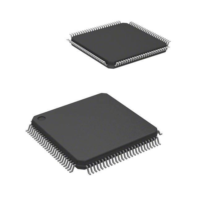


 工商网监
湘ICP备2023018690号
工商网监
湘ICP备2023018690号
