TPD2007F
TOSHIBA Intelligent Power Device Silicon Monolithic Power MOS Integrated Circuit
TPD2007F
Low-Side Power Switch Array (8 Channels) for Motors, Solenoids, and Lamp Drivers
The TPD2007F is an 8-channel low-side switch array. The IC has a vertical MOSFET output which can be directly driven from a CMOS or TTL logic circuit (e.g., an MPU). It offers overcurrent and overtemperature protection functions.
Features
• • • • • • • • • 8-channel low-side switch array incorporating an N-channel power MOSFET (1.4Ω max) Can directly drive a power load from a microprocessor. Built-in protection against overtemperature and overcurrent 8-channel access enables space-saving design. High operating voltage: 40 V Low on-resistance: 1.4 Ω max @VIN = 5 V, ID = 0.5 A (per channel) Supports parallel operation. Built-in active clamp circuit Supplied in an SSOP-24 package (300 mil) in embossed taping. Weight: 0.29 g (typ.)
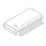
Pin Assignment
Marking
Lot No. A dot indicates lead (Pb)-free package or lead (Pb)-free finish.
TPD2007F
Part No. (or abbreviation code)
Note: This product has a MOS structure and is sensitive to electrostatic discharge. When handling this product, ensure that the environment is protected against electrostatic discharge.
1
2006-10-31
�TPD2007F
Block Diagram
2
2006-10-31
�TPD2007F
Pin Description
Pin No. 1 2 3 4 5 6 7 8 9 10 11 12 13 14 15 16 17 18 19 20 21 22 23 24 Symbol GND N.C. IN1 IN2 IN3 IN4 IN5 IN6 IN7 IN8 N.C. GND N.C. N.C. OUT8 OUT7 OUT6 OUT5 OUT4 OUT3 OUT2 OUT1 N.C. N.C. Output pin for channel 8 Output pin for channel 7 Output pin for channel 6 Output pin for channel 5 Output pin for channel 4 Output pin for channel 3 Output pin for channel 2 Output pin for channel 1 ― ― GND pin; in common with the pin no.1 internally. ― ― Description GND pin; in common with the pin no.12 internally. ― Control input pin for channel 1 and built-in pull-down resistor (300 kΩ typ.) Control input pin for channel 2 and built-in pull-down resistor (300 kΩ typ.) Control input pin for channel 3 and built-in pull-down resistor (300 kΩ typ.) Control input pin for channel 4 and built-in pull-down resistor (300 kΩ typ.) Control input pin for channel 5 and built-in pull-down resistor (300 kΩ typ.) Control input pin for channel 6 and built-in pull-down resistor (300 kΩ typ.) Control input pin for channel 7 and built-in pull-down resistor (300 kΩ typ.) Control input pin for channel 8 and built-in pull-down resistor (300 kΩ typ.) ―
Timing Chart
Note: The overheating detector circuits feature hysteresis. After overheating is detected, normal operation is restored only when the junction temperature falls by the hysteresis amount (10°C typ.) in relation to the overheating detection temperature.
3
2006-10-31
�TPD2007F
Truth Table
Input Signal L H L H L H Output Signal H L H Internally limited H H State Normal
Overcurrent protection
Overtemperature protection
Absolute Maximum Ratings (Ta = 25°C)
Characteristic Drain-source voltage Input voltage Output current Power dissipation (operating all channels, ta = 25°C) Single pulse avalanche energy Operating temperature Junction temperature Storage temperature Symbol VDSS VIN ID PT EAS Topr Tj Tstg Rating 40 −0.5 ~ 7 Internally Limited 0.8 1.2 (Note) 10 −40 ~ 85 150 −55 ~ 150 Unit V V A W mJ °C °C °C
Note: Using continuously under heavy loads (e.g. the application of high temperature/current/voltage and the significant change in temperature, etc.) may cause this product to decrease in the reliability significantly even if the operating conditions (i.e. operating temperature/current/voltage, etc.) are within the absolute maximum ratings and the operating ranges. Please design the appropriate reliability upon reviewing the Toshiba Semiconductor Reliability Handbook (“Handling Precautions”/Derating Concept and Methods) and individual reliability data (i.e. reliability test report and estimated failure rate, etc).
Thermal Characteristics
Characteristic Thermal resistance junction to ambient (operating all channels, ta = 25°c) Symbol ΣRth (j-a) Rating 156.3 104.2 (Note) Unit °C / W
Note: 60 mm × 60 mm × 1.6 mm when mounted on a glass epoxy PCB (DC)
4
2006-10-31
�TPD2007F
Electrical Characteristics
Characteristic Drain-source clamp voltage Input voltage Input current On resistance Off current
(Unless otherwise specified, Tj = 25°C)
Symbol V (BR) DSS Vth IIL IIH RDS(ON) IDSS IS(1) Overcurrent protection IS(2) Overtemperature Protection Switching time Operating input voltage protection circuit Drain-source diode forward voltage Temperature Hysteresis TSD ΔTSD tON tOFF VIN(P) VDSF ― ― ― 1 1 ― ― Test Circuit ― ― ― ― ― ― ― Test Condition ID = 10 mA, VIN = 0 V VDS = 24 V, IDS = 1 mA VIN = 0 V VIN = 5 V VIN = 5 V, IO = 0.5 A VDS = 40V VDS = 12 V, VIN = 5 V, RL = 3Ω VDS = 30 V, VIN = 5 V, RL = 3Ω VIN = 5 V ― VDD = 12 V, RL = 24Ω, VIN = 0 V / 5 V ― IF = 1 A, VIN = 0 V Min 40 0.8 −10 ― ― ― 1 0.7 ― ― ― ― 3.9 ― Typ. ― ― ― 140 1.0 ― 2 ― 160 10 10 10 ― ― Max ― 2.0 10 300 1.4 100 3 A 2 ― ― 50 50 6.0 1.6 °C Unit V V μA Ω μA
μs V V
Description of Protector Circuit
(1) Overtemperature Protection
• The overheating detector circuits feature hysteresis. After overheating is detected, normal operation is restored only when the junction temperature falls by the hysteresis amount (10°C typ.) in relation to the overheating detection temperature.
(2)
Overcurrent Protection
• When overcurrent is detected, the overcurrent limiter function limits the output current. Normal operation is restored when the load current drops below the overcurrent detection value.
Test Circuit
Switching Time
5
2006-10-31
�TPD2007F
Tj = 25℃
Tj = 85℃
Tj = 25℃
Tj = 25℃
6
2006-10-31
�TPD2007F
7
2006-10-31
�TPD2007F
Moisture-Proof Packing
After the pack is opened, the devices should be used within 48 hours and in a 30°C, 60% RH environment. Embossed-tape packing cannot be baked. Devices so packed must be within their allowable time limits after unpacking, as specified on the packing. Standard tape packing quantity: 2000 devices / reel (EL1)
8
2006-10-31
�TPD2007F
Package Dimensions
Weight: 0.29 g (typ.)
9
2006-10-31
�TPD2007F
RESTRICTIONS ON PRODUCT USE
• The information contained herein is subject to change without notice.
20070701-EN
• TOSHIBA is continually working to improve the quality and reliability of its products. Nevertheless, semiconductor devices in general can malfunction or fail due to their inherent electrical sensitivity and vulnerability to physical stress. It is the responsibility of the buyer, when utilizing TOSHIBA products, to comply with the standards of safety in making a safe design for the entire system, and to avoid situations in which a malfunction or failure of such TOSHIBA products could cause loss of human life, bodily injury or damage to property. In developing your designs, please ensure that TOSHIBA products are used within specified operating ranges as set forth in the most recent TOSHIBA products specifications. Also, please keep in mind the precautions and conditions set forth in the “Handling Guide for Semiconductor Devices,” or “TOSHIBA Semiconductor Reliability Handbook” etc. • The TOSHIBA products listed in this document are intended for usage in general electronics applications (computer, personal equipment, office equipment, measuring equipment, industrial robotics, domestic appliances, etc.).These TOSHIBA products are neither intended nor warranted for usage in equipment that requires extraordinarily high quality and/or reliability or a malfunction or failure of which may cause loss of human life or bodily injury (“Unintended Usage”). Unintended Usage include atomic energy control instruments, airplane or spaceship instruments, transportation instruments, traffic signal instruments, combustion control instruments, medical instruments, all types of safety devices, etc.. Unintended Usage of TOSHIBA products listed in his document shall be made at the customer’s own risk. • The products described in this document shall not be used or embedded to any downstream products of which manufacture, use and/or sale are prohibited under any applicable laws and regulations. • The information contained herein is presented only as a guide for the applications of our products. No responsibility is assumed by TOSHIBA for any infringements of patents or other rights of the third parties which may result from its use. No license is granted by implication or otherwise under any patents or other rights of TOSHIBA or the third parties. • Please contact your sales representative for product-by-product details in this document regarding RoHS compatibility. Please use these products in this document in compliance with all applicable laws and regulations that regulate the inclusion or use of controlled substances. Toshiba assumes no liability for damage or losses occurring as a result of noncompliance with applicable laws and regulations.
10
2006-10-31
�